
W942508CH
8M
◊ 4 BANKS ◊ 8 BIT DDR SDRAM
Publication Release Date: May 21, 2003
- 1 -
Revision A3
Table of Contents-
1.
GENERAL DESCRIPTION .................................................................................................. 3
2.
FEATURES .......................................................................................................................... 3
3.
KEY PARAMETERS ............................................................................................................ 4
4.
PIN CONFIGURATION ........................................................................................................ 5
5.
PIN DESCRIPTION.............................................................................................................. 6
6.
BLOCK DIAGRAM ............................................................................................................... 7
7.
ELECTRICAL CHARACTERISTICS .................................................................................... 8
7.1
Absolute Maximum Ratings ................................................................................................. 8
7.2
Recommended DC Operating Conditions............................................................................ 8
7.3
Capacitance ......................................................................................................................... 9
7.4
Leakage and Output Buffer Characteristics ......................................................................... 9
7.5
DC Characteristics ............................................................................................................. 10
7.6
AC Characteristics and Operating Condition ..................................................................... 11
7.7
AC Test Conditions ............................................................................................................ 13
8.
Operation Mode ................................................................................................................. 15
8.1
Simplified Truth Table ........................................................................................................ 15
8.2
Function Truth Table .......................................................................................................... 16
8.3
Function Truth Table for CKE ............................................................................................ 19
8.4
Simplified State Diagram.................................................................................................... 20
9.
FUNCTIONAL DESCRIPTION........................................................................................... 21
9.1
Power Up Sequence .......................................................................................................... 21
9.2
Command Function............................................................................................................ 21
9.3
Read Operation.................................................................................................................. 24
9.4
Write Operation .................................................................................................................. 24
9.5
Precharge........................................................................................................................... 24
9.6
Burst Termination............................................................................................................... 25
9.7
Refresh Operation.............................................................................................................. 25
9.8
Power Down Mode............................................................................................................. 25
9.9
Mode Register Operation ................................................................................................... 25
10.
TIMING WAVEFORMS ............................................................................................................. 29
10.1
Command Input Timing...................................................................................................... 29
10.2
Timing of the CLK Signals.................................................................................................. 29
10.3
Read Timing (Burst Length = 4)......................................................................................... 30
10.4
Write Timing (Burst Length = 4) ......................................................................................... 31
10.5
DM, DATA MASK (W942508CH/W942504CH) ................................................................. 32

W942508CH
- 2 -
10.6
DM, DATA MASK (W942516CH)....................................................................................... 32
10.7
Mode Register Set (MRS) Timing ...................................................................................... 33
10.8
Extend Mode Register Set (EMRS) Timing........................................................................ 34
10.9
Auto Precharge Timing (Read Cycle, CL = 2).................................................................... 35
10.10
Auto Precharge Timing (Write Cycle)................................................................................. 37
10.11
Read Interrupted by Read (CL = 2, BL = 2, 4, 8) ............................................................... 38
10.12
Burst Read Stop (BL = 8)................................................................................................... 38
10.13
Read Interrupted by Write & BST (BL = 8)......................................................................... 39
10.14
Read Interrupted by Precharge (BL = 8)............................................................................ 39
10.15
Write Interrupted by Write (BL = 2, 4, 8) ............................................................................ 40
10.16
Write Interrupted by Read (CL = 2, BL = 8) ....................................................................... 40
10.17
Write Interrupted by Read (CL = 2.5, BL = 4) .................................................................... 41
10.18
Write Interrupted by Precharge (BL = 8) ............................................................................ 41
10.19
2 Bank Interleave Read Operation (CL = 2, BL = 2) .......................................................... 42
10.20
2 Bank Interleave Read Operation (CL = 2, BL = 4) .......................................................... 42
10.21
4 Bank Interleave Read Operation (CL = 2, BL = 2) .......................................................... 43
10.22
4 Bank Interleave Read Operation (CL = 2, BL = 4) .......................................................... 43
10.23
Auto Refresh Cycle ............................................................................................................ 44
10.24
Active Power Down Mode Entry and Exit Timing............................................................... 44
10.25
Precharged Power Down Mode Entry and Exit Timing ...................................................... 44
10.26
Self Refresh Entry and Exit Timing .................................................................................... 45
11.
PACKAGE DIMENSION ........................................................................................................... 46
11.1
TSOP 66l ≠ 400 mil ............................................................................................................ 46
12.
REVISION HISTORY ................................................................................................................ 47

W942508CH
Publication Release Date: May 21, 2003
- 3 -
Revision A3
1. GENERAL DESCRIPTION
W942508CH is a CMOS Double Data Rate synchronous dynamic random access memory (DDR
SDRAM), organized as 8,388,608 words
◊ 4 banks ◊ 8 bits. Using pipelined architecture and 0.13 µm
process technology, W942508CH delivers a data bandwidth of up to 400M words per second (-5). To
fully comply with the personal computer industrial standard, W942508CH is sorted into four speed
grades: -5, -6, -7, -75 The -5 is compliant to the 200MHz/CL2.5 & CL3 specification, The -6 is
compliant to the 166MHz/CL2.5 specification, the -7 is compliant to the 143MHz/CL2.5 or
DDR266/CL2 specification, the -75 is compliant to the DDR266/CL2.5 specification.
All Inputs reference to the positive edge of CLK (except for DQ, DM, and CKE). The timing reference
point for the differential clock is when the CLK and
CLK
signals cross during a transition. And Write
and Read data are synschronized with the both edges of DQS (Data Strobe).
By having a programmable Mode Register, the system can change burst length, latency cycle,
interleave or sequential burst to maximize its performance. W942508CH is ideal for main memory in
high performance applications.
2. FEATURES
∑ 2.5V ±0.2V Power Supply for DDR266
∑ 2.5V ±0.2V Power Supply for DDR333
∑ 2.6V ±0.1V Power Supply for DDR400
∑ Up to 200 MHz Clock Frequency
∑ Double Data Rate architecture; two data transfers per clock cycle
∑ Differential clock inputs (CLK and
CLK
)
∑ DQS is edge-aligned with data for Read; center-aligned with data for Write
∑ CAS Latency: 2, 2.5 and 3
∑ Burst Length: 2, 4 and 8
∑ Auto Refresh and Self Refresh
∑ Precharged Power Down and Active Power Down
∑ Write Data Mask
∑ Write Latency = 1
∑ 8K Refresh cycles / 64 mS
∑ Interface: SSTL-2
∑ Packaged in TSOP II 66-pin, 400 x 875mil, 0.65mm pin pitch
W942508CH
- 4 -
3. KEY PARAMETERS
SYMBOL
DESCRIPTION
MIN./MAX.
-7
-75
CL = 2
Min.
7.5 nS
8 nS
t
CK
Clock Cycle Time
CL = 2.5
Min.
7 nS
7.5 nS
t
RAS
Active to Precharge Command Period
Min.
45 nS
45 nS
t
RC
Active to Ref/Active Command Period
Min.
65 nS
65 nS
I
DD1
OPERATION CURRENT (SINGLE BANK)
Max.
120 mA
120 mA
I
DD4
Burst Operation Current
Max.
165 mA
155 mA
I
DD6
SELF-REFRESH CURRENT
Max.
3 mA
3 mA
SYMBOL
DESCRIPTION
MIN./MAX.
-5
-6
CL = 2.5
Min.
5 nS
6 nS
t
CK
Clock Cycle Time
CL = 3
Min.
5 nS
6 nS
t
RAS
Active to Precharge Command Period
Min.
40 nS
42 nS
t
RC
Active to Ref/Active Command Period
Min.
55 nS
60 nS
I
DD1
OPERATION CURRENT (SINGLE BANK)
Max.
120 mA
120 mA
I
DD4
Burst Operation Current
Max.
165 mA
165 mA
I
DD6
SELF-REFRESH CURRENT
Max.
3 mA
3 mA
W942508CH
Publication Release Date: May 21, 2003
- 5 -
Revision A3
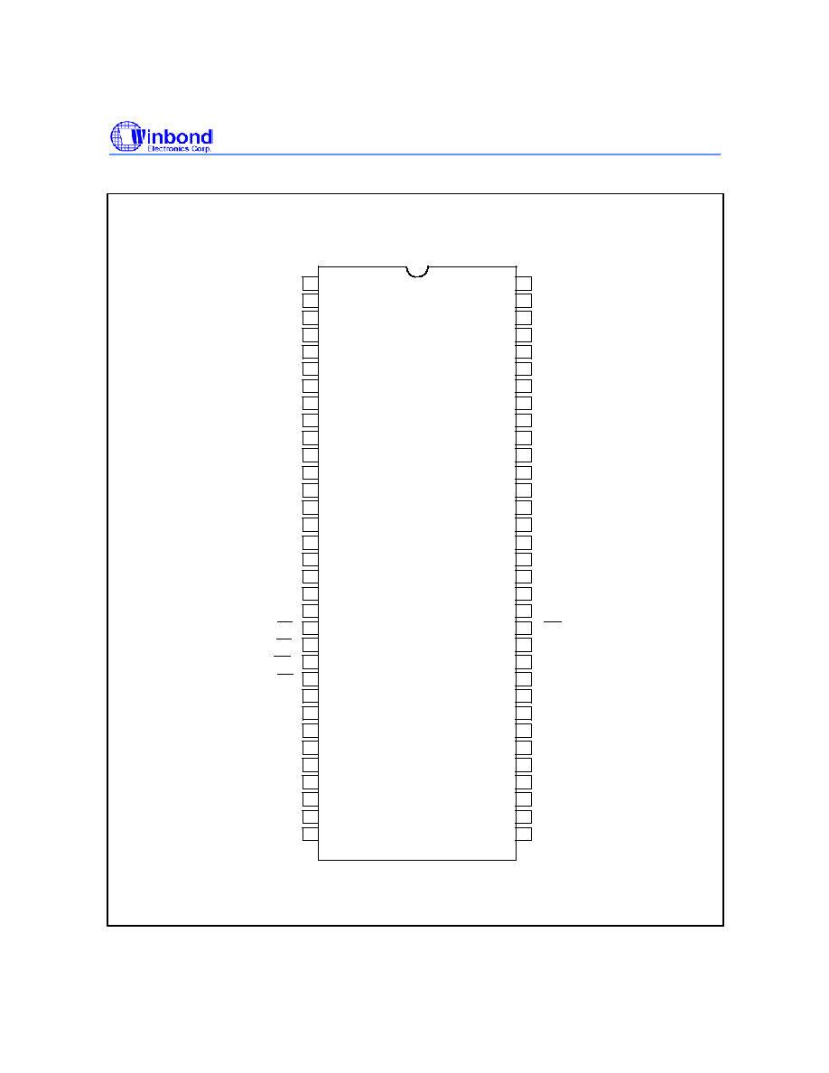
4. PIN CONFIGURATION
V
SS
DQ7
V
SS
Q
NC2
DQ6
V
DD
Q
NC2
DQ5
V
SS
Q
NC2
DQ4
V
DD
Q
NC2
V
SS
NC1
DQS
CLK
CKE
A11
A9
A8
A7
A6
A5
A4
V
SS
66
65
64
63
62
61
60
59
58
57
56
55
54
53
52
51
50
49
48
47
46
45
44
43
42
41
40
1
2
3
4
5
6
7
8
9
10
11
12
13
14
15
16
17
18
19
20
21
22
23
24
25
26
27
V
DD
DQ0
V
DD
Q
NC2
DQ1
V
SS
Q
NC2
DQ2
V
DD
Q
NC2
DQ3
V
SS
Q
NC2
NC1
V
DD
Q
BS0
BS1
A10/AP
A0
A1
A2
A3
CS
RAS
CAS
WE
28
29
30
31
32
33
39
38
37
36
35
34
V
DD
NC2
NC1
NC2
NC1
V
DD
NC1
V
SS
Q
NC1
A12
NC1
CLK
DM
V
REF