
W986416DH
1M
◊
4 BANKS
◊
16 BITS SDRAM
Publication Release Date: April 11, 2002
- 1 - Revision A4
Table of Contents-
1. GENERAL DESCRIPTION ..................................................................................................................3
2. FEATURES ..........................................................................................................................................3
3. AVAILABLE PART NUMBER...............................................................................................................3
4. PIN CONFIGURATION ........................................................................................................................4
5. PIN DESCRIPTION..............................................................................................................................5
6. BLOCK DIAGRAM ...............................................................................................................................6
7. FUNCTIONAL DESCRIPTION ............................................................................................................7
Power Up and Initialization................................................................................................................7
Programming Mode Register............................................................................................................7
Bank Activate Command ..................................................................................................................7
Read and Write Access Modes ........................................................................................................7
Burst Read Command ......................................................................................................................8
Burst Command................................................................................................................................8
Read Interrupted by a Read..............................................................................................................8
Read Interrupted by a Write..............................................................................................................8
Write Interrupted by a Write..............................................................................................................8
Write Interrupted by a Read..............................................................................................................8
Burst Stop Command .......................................................................................................................8
Addressing Sequence of Sequential Mode.......................................................................................9
Addressing Sequence of Interleave Mode ........................................................................................9
Auto-precharge Command ...............................................................................................................9
Precharge Command......................................................................................................................10
Self Refresh Command ..................................................................................................................10
Power Down Mode..........................................................................................................................10
No Operation Command.................................................................................................................11
Deselect Command ........................................................................................................................11
Clock Suspend Mode......................................................................................................................11
8. TABLE OF OPERATING MODES .....................................................................................................12
Simplified State Diagram ................................................................................................................13
9. DC CHARACTERISTICS ...................................................................................................................14
Absolute Maximum Rating..............................................................................................................14
10. RECOMMENDED DC OPERATING CONDITIONS ........................................................................14

W986416DH
- 2 -
11. CAPACITANCE................................................................................................................................14
12. DC CHARACTERISTICS .................................................................................................................15
13. AC CHARACTERISTICS .................................................................................................................16
14. TIMING WAVEFORMS....................................................................................................................19
Command Input Timing ..................................................................................................................19
Read Timing ...................................................................................................................................20
Control Timing of Input Data...........................................................................................................21
Control Timing of Output Data ........................................................................................................22
Mode Register Set Cycle ................................................................................................................23
15. OPERATING TIMING EXAMPLE ....................................................................................................24
Interleaved Bank Read (Burst Length = 4, CAS Latency = 3) ........................................................24
Interleaved Bank Read (Burst Length = 4, CAS Latency = 3, Autoprecharge)...............................25
Interleaved Bank Read (Burst Length = 8, CAS Latency = 3) ........................................................26
Interleaved Bank Read (Burst Length = 8, CAS Latency = 3, Autoprecharge)...............................27
Interleaved Bank Write (Burst Length = 8) .....................................................................................28
Interleaved Bank Write (Burst Length = 8, Autoprecharge)............................................................29
Page Mode Read (Burst Length = 4, CAS Latency = 3) .................................................................30
Page Mode Read/Write (Burst Length = 8, CAS Latency = 3) .......................................................31
Autoprecharge Read (Burst Length = 4, CAS Latency = 3)............................................................32
Autoprecharge Write (Burst Length = 4).........................................................................................33
Autorefresh Cycle ...........................................................................................................................34
Self-refresh Cycle ...........................................................................................................................35
Bust Read and Single Write (Burst Length = 4, CAS Latency = 3).................................................36
Power-down Mode ..........................................................................................................................37
Auto-precharge Timing (Write Cycle) .............................................................................................38
Auto-precharge Timing (Read Cycle) .............................................................................................39
Timing Chart of Read to Write Cycle ..............................................................................................40
Timing Chart of Write to Read Cycle ..............................................................................................41
Timing Chart of Burst Stop Cycle (Burst Stop Command) .............................................................42
Timing Chart of Burst Stop Cycle (Precharge Command)..............................................................43
CKE/DQM Input Timing (Write Cycle) ............................................................................................44
CKE/DQM Input Timing (Read Cycle) ............................................................................................45
Self Refresh/Power Down Mode Exit Timing..................................................................................46
16. PACKAGE DIMENSION ..................................................................................................................47
54L TSOP (II)-400 mil.....................................................................................................................47
17. VERSION HISTORY ........................................................................................................................48
W986416DH
Publication Release Date: April 11, 2002
- 3 - Revision A4
1. GENERAL DESCRIPTION
W986416DH is a high-speed synchronous dynamic random access memory (SDRAM), organized as
1M words x 4 banks x 16 bits. Using pipelined architecture and 0.175
µ
m process technology,
W986416DH delivers a data bandwidth of up to 400M bytes per second (-5). For different application,
W986416DH is sorted into the following speed grades: -5, -6, -7. The -5 parts can run up to 200
MHz/CL3. The -6 parts can run up to 166 MHz/CL3. The -7 parts can run up to 143 MHz/CL3. For
handheld device application, we also provide a low power option, the grade of -7L, with Self Refresh
Current under 400
µ
A and work well at 2.7V during Self Refresh Mode. For special application, we
provide extended temperature option the grade of -6I can work well in wide temperature from -40
∞
C to
85
∞
C.
Accesses to the SDRAM are burst oriented. Consecutive memory location in one page can be
accessed at a burst length of 1, 2, 4, 8 or full page when a bank and row is selected by an ACTIVE
command. Column addresses are automatically generated by the SDRAM internal counter in burst
operation. Random column read is also possible by providing its address at each clock cycle. The
multiple bank nature enables interleaving among internal banks to hide the precharging time.
By having a programmable Mode Register, the system can change burst length, latency cycle,
interleave or sequential burst to maximize its performance. W986416DH is ideal for main memory in
high performance applications.
2. FEATURES
∑
3.3V
±
0.3V power supply
∑
1048576 words
x 4 banks x 16 bits organization
∑
Self Refresh Current: Standard and Low Power
∑
CAS latency: 2 and 3
∑
Burst Length: 1, 2, 4, 8, and full page
∑
Sequential and Interleave burst
∑
Burst read, single write operation
∑
Byte data controlled by DQM
∑
Power-down Mode
∑
Auto-precharge and controlled precharge
∑
4K refresh cycles/64 mS
∑
Interface: LVTTL
∑
Packaged in TSOP II 54-pin, 400 mil - 0.80
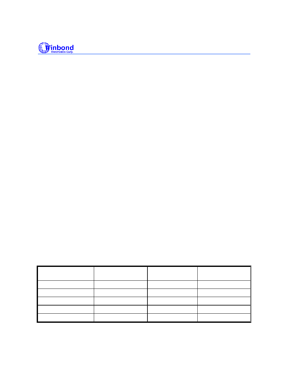
3. AVAILABLE PART NUMBER
PART NUMBER
SPEED (CL = 3)
SELF REFRESH
CURRENT (MAX.)
OPERATING
TEMPERATURE
W986416DH-5
200 MHz
1 mA
0
∞
C
-
70
∞
C
W986416DH-6
166 MHz
1 mA
0
∞
C
-
70
∞
C
W986416DH-6I
166 MHz
400
µ
A
-40
∞
C
-
85
∞
C
W986416DH-7
143 MHz
1 mA
0
∞
C
-
70
∞
C
W986416DH-7L
143 MHz
400
µ
A
0
∞
C
-
70
∞
C
W986416DH
- 4 -
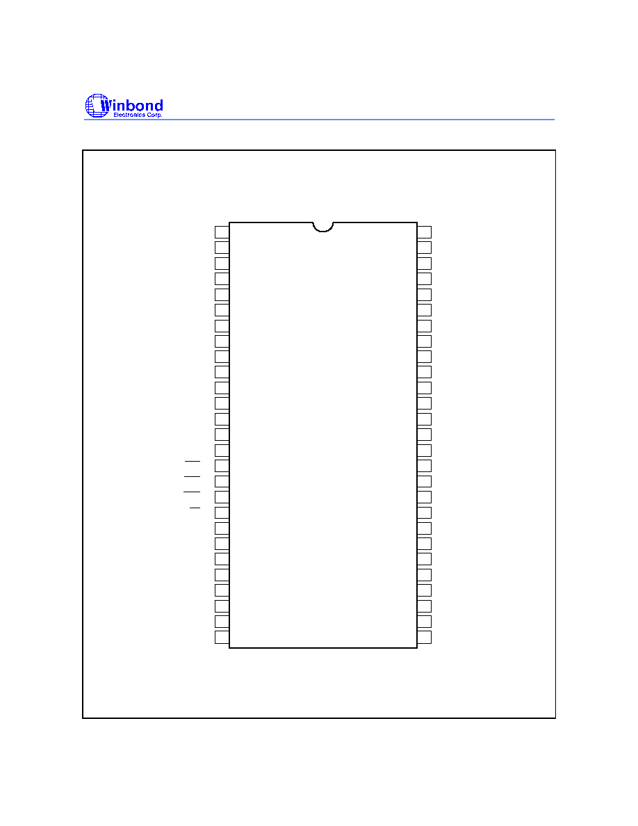
4. PIN CONFIGURATION
54
53
52
51
50
49
48
47
46
45
44
43
42
41
40
39
38
37
36
35
34
33
32
31
30
29
28
1
2
3
4
5
6
7
8
9
10
11
12
13
14
15
16
17
18
19
20
21
22
23
24
25
26
27
D Q 0
D Q 1
D Q 2
D Q 3
D Q 4
D Q 5
D Q 6
D Q 7
L D Q M
CAS
RAS
C S
B S 0
B S 1
A10/AP
A0
A1
A2
A3
D Q 1 5
D Q 1 4
D Q 1 3
D Q 1 2
D Q 1 1
D Q 1 0
D Q 9
D Q 8
N C
U D Q M
CLK
C K E
N C
A11
A9
A8
A7
A6
A5
A4
V
C C
V
C C
Q
V
C C
Q
V
S S
Q
V
S S
Q
V
C C
V
C C
V
S S
V
S S
Q
V
C C
Q
V
S S
Q
V
C C
Q
V
S S
V
S S
W E
W986416DH
Publication Release Date: April 11, 2002
- 5 - Revision A4
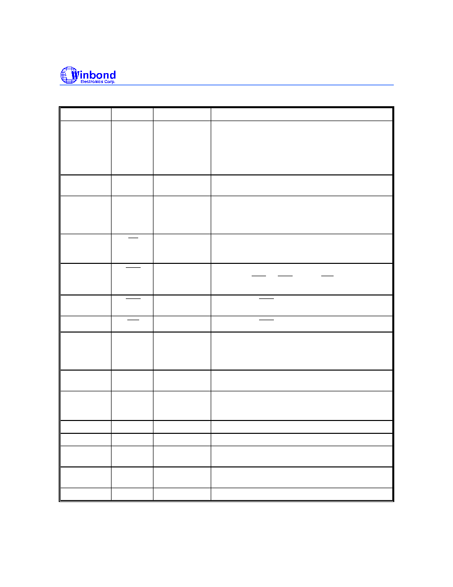
5. PIN DESCRIPTION
PIN NUMBER PIN NAME FUNCTION
DESCRIPTION
23
-
26, 22,
29
-
35
A0
-
A11 Address
Multiplexed pins for row and column address.
Row address: A0
-
A11. Column address: A0
-
A7.
A10 is sampled during a precharge command to
determine if all banks are to be precharged or bank
selected by BS0, BS1.
20, 21
BS0, BS1 Bank Select
Select bank to activate during row address latch time,
or bank to read/write during address latch time.
2, 4, 5, 7, 8,
10, 11, 13, 42,
44, 45, 47, 48,
50, 51, 53
DQ0
-
DQ15
Data Input/
Output
Multiplexed pins for data output and input.
19
CS
Chip Select
Disable or enable the command decoder. When
command decoder is disabled, new command is
ignored and previous operation continues.
18
RAS
Row Address
Strobe
Command input. When sampled at the rising edge of
the clock RAS , CAS and WE define the
operation to be executed.
17
CAS
Column
Address Strobe
Referred to RAS
16
WE
Write Enable
Referred to RAS
39, 15
UDQM
LDQM
Input/output
Mask
The output buffer is placed at Hi-Z (with latency of 2)
when DQM is sampled high in read cycle. In write
cycle, sampling DQM high will block the write
operation with zero latency.
38
CLK
Clock Inputs
System clock used to sample inputs on the rising edge
of clock.
37
CKE
Clock Enable CKE controls the clock activation and deactivation.
When CKE is low, Power Down mode, Suspend
mode, or Self Refresh mode is entered.
1, 14, 27
V
CC
Power (+3.3V) Power for input buffers and logic circuit inside DRAM.
28, 41, 54
V
SS
Ground
Ground for input buffers and logic circuit inside DRAM.
3, 9, 43, 49
V
CCQ
Power (+3.3V)
for I/O Buffer
Separated power from V
CC
, to improve DQ noise
immunity.
6, 12, 46, 52
V
SSQ
Ground for I/O
Buffer
Separated ground from V
SS
, to improve DQ noise
immunity.
36, 40
NC
No Connection No connection