 | –≠–ª–µ–∫—Ç—Ä–æ–Ω–Ω—ã–π –∫–æ–º–ø–æ–Ω–µ–Ω—Ç: W987Y6CBN | –°–∫–∞—á–∞—Ç—å:  PDF PDF  ZIP ZIP |

Preliminary W987Y6CB
2M
◊
4 BANKS
◊
16 BIT SDRAM
Publication Release Date: May 21, 2002
- 1 - Revision A1
Table of Contents-
1. GENERAL DESCRIPTION ..................................................................................................................3
2. FEATURES ..........................................................................................................................................3
3. AVAILABLE PART NUMBER ..............................................................................................................3
4. BALL CONFIGURATION .....................................................................................................................4
5. BALL DESCRIPTION...........................................................................................................................5
6. BLOCK DIAGRAM ...............................................................................................................................6
7. ABSOLUTE MAXIMUM RATINGS ......................................................................................................7
8. DC ELECTRICAL CHARACTERISTICS AND OPERATING CONDITIONS.......................................7
9. CAPACITANCE ...................................................................................................................................8
10. OPERATING CURRENT ...................................................................................................................8
11. AC CHARACTERISTICS AND OPERATING CONDITION...............................................................9
12. FUNCTIONAL DESCRIPTION ........................................................................................................12
Power Up Sequence.......................................................................................................................12
Command Function ........................................................................................................................12
Read Operation ..............................................................................................................................15
Write Operation...............................................................................................................................15
Precharge .......................................................................................................................................15
Burst Termination ...........................................................................................................................15
Interruption......................................................................................................................................16
Refresh Operation ..........................................................................................................................16
Power Down Mode .........................................................................................................................17
Mode Register Set Operation .........................................................................................................17
Simplified State Diagram ................................................................................................................19
13. TIMING WAVEFORMS....................................................................................................................20
Command Input Timing ..................................................................................................................20
Read Timing ...................................................................................................................................21
Control Timing of Input / Output Data.............................................................................................22
14. OPERATING TIMING EXAMPLE ....................................................................................................24
Interleaved Bank Read (Burst Length = 4, CAS Latency = 3)........................................................24
Interleaved Bank Read (Burst Length = 4, CAS Latency = 3, Autoprecharge) ..............................25

Preliminary W987Y6CB
- 2 -
Interleaved Bank Read (Burst Length = 8, CAS Latency = 3)........................................................26
Interleaved Bank Read (Burst Length = 8, CAS Latency = 3, Autoprecharge) ..............................27
Interleaved Bank Write (Burst Length = 8) .....................................................................................28
Interleaved Bank Write (Burst Length = 8, Autoprecharge) ...........................................................29
Page Mode Read (Burst Length = 4, CAS Latency = 3) ................................................................30
Page Mode Read / Write (Burst Length = 8, CAS Latency = 3) .....................................................31
Auto Precharge Read (Burst Length = 4, CAS Latency = 3)..........................................................32
Auto Precharge Write (Burst Length = 4) .......................................................................................33
Auto Refresh Cycle.........................................................................................................................34
Self Refresh Cycle ..........................................................................................................................35
Burst Read and Single Write (Burst Length = 4, CAS Latency = 3) ...............................................36
PowerDown Mode ..........................................................................................................................37
Autoprecharge Timing (Read Cycle) ..............................................................................................38
Autoprecharge Timing (Write Cycle) ..............................................................................................39
Timing Chart of Read to Write Cycle ..............................................................................................40
Timing Chart of Write to Read Cycle ..............................................................................................40
Timing Chart of Burst Stop Cycle (Burst Stop Command) .............................................................41
Timing Chart of Burst Stop Cycle (Precharge Command) .............................................................41
CKE/DQM Input Timing (Write Cycle) ............................................................................................42
CKE/DQM Input Timing (Read Cycle) ............................................................................................43
Self Refresh/Power Down Mode Exit Timing..................................................................................44
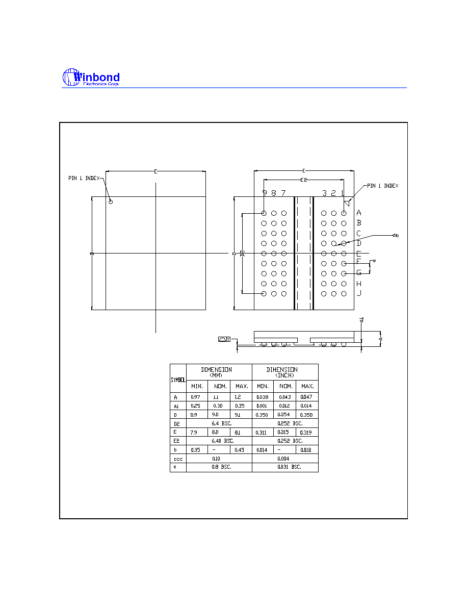
15. PACKAGE DIMENSION ..................................................................................................................45
16. REVISION HISTORY.......................................................................................................................46
Preliminary W987Y6CB
Publication Release Date: May 21, 2002
- 3 - Revision A1
1. GENERAL DESCRIPTION
W987Y6CB is a high-speed synchronous dynamic random access memory (SDRAM), organized as
2M words
◊
4 banks
◊
16 bits. Using pipelined architecture and 0.175
µ
m process technology,
W987Y6CB delivers a data bandwidth of up to 125M words per second (-8). For different application,
W987Y6CB is sorted into two speed grades: -75 and -8. The -75 is compliant to the 133 MHz/ CL3
specification; the -8 is compliant to the 125 MHz/ CL3 specification. For handheld device application,
these parts are specially designed with several power saving mechanisms to achieve extremely low
Self Refresh Current.
Accesses to the SDRAM are burst oriented. Consecutive memory location in one page can be
accessed at a burst length of 1, 2, 4, 8 or full page when a bank and row is selected by an ACTIVE
command. Column addresses are automatically generated by the SDRAM internal counter in burst
operation. Random column read is also possible by providing its address at each clock cycle. The
multiple bank nature enables interleaving among internal banks to hide the precharging time.
By having a programmable Mode Register, the system can change burst length, latency cycle,
interleave or sequential burst to maximize its performance. W987Y6CB is ideal for main memory in
high performance applications.
2. FEATURES
∑
Power supply V
DD
= 2.5V
±
0.2V
∑
V
DDQ
= 2.5V
∑
Standard Self Refresh Mode
∑
Power Down Mode
∑
CAS Latency: 2 and 3
∑
Burst Length: 1, 2, 4, 8, and full page
∑
4K Refresh Cycles / 64 mS
∑
Interface: LVTTL
∑
Packaged in 54 balls FBGA
∑
Operating Temperature Range
∑
Commercial Temperature (0
∞
C
-
70
∞
C)
∑
Industrial Temperature (-40
∞
C
-
85
∞
C)
3. AVAILABLE PART NUMBER
PART NUMBER
SPEED
SELF REFRESH
CURRENT (MAX.)
TEMPERATURE
RANGE
LEAD-FREE
PACKAGE
W987Y6CBN75 133 MHz/ CL3
400
µ
A
0
∞
C
-
70
∞
C
No
W987Y6CBG75 133 MHz/ CL3
400
µ
A
0
∞
C
-
70
∞
C
Yes
W987Y6CBN80 125 MHz/ CL3
400
µ
A
0
∞
C
-
70
∞
C
No
W987Y6CBG80 125 MHz/ CL3
400
µ
A
0
∞
C
-
70
∞
C
Yes
Preliminary W987Y6CB
- 4 -
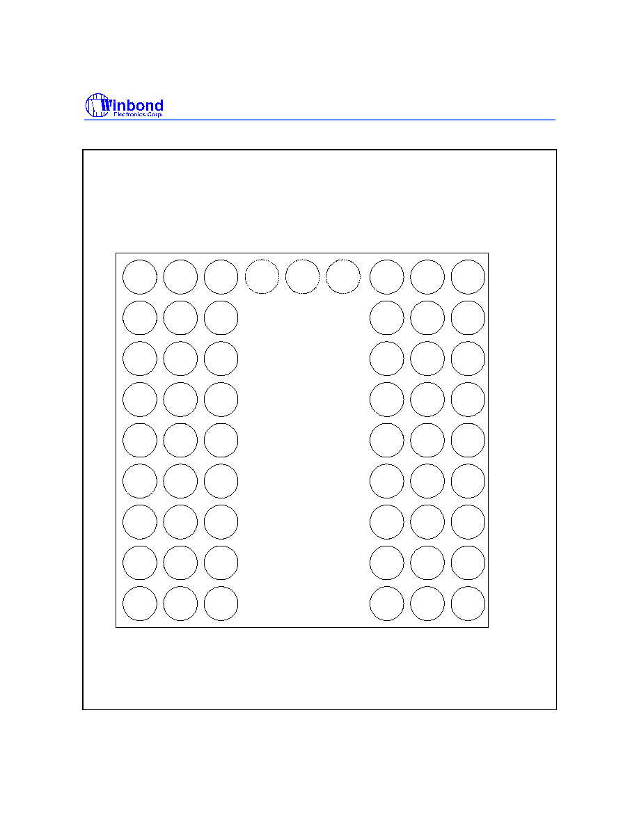
4. BALL CONFIGRUATION
1
2
3
4
5
6
7
8
9
A
B
C
D
E
F
G
H
J
(TOP VIEW)
V
DD
DQ7
DQ1
DQ3
DQ5
WE
CS
A10/
AP
V
DD
Vss
DQ8
DQ14
DQ12
DQ10
UDQM
NC
A8
Vss
DQ0
LDQM
DQ2
DQ4
DQ6
RAS
BA1
A1
A2
DQ15
NC
DQ13
DQ11
DQ9
CLK
A11
A7
A5
V
DD
Q
V
DD
CAS
BA0
A0
A3
V
SS
Q
V
DD
Q
V
SS
Q
V
SS
Q
V
SS
V
DD
Q
V
SS
Q
V
DD
Q
CKE
A9
A6
A4
Package Dimension 8mm x 9 mm
Preliminary W987Y6CB
Publication Release Date: May 21, 2002
- 5 - Revision A1
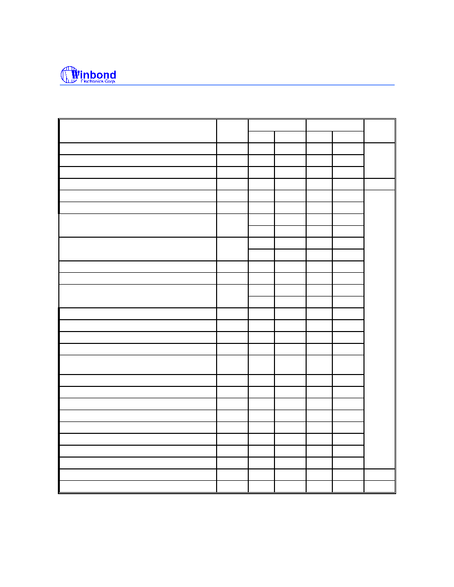
5. BALL DESCRIPTION
PIN NUMBER BALL NAME FUNCTION
DESCRIPTION
H7, H8, J8, J7,
J3, J2, H3, H2,
H1, G3, H9, G2
A0
-
A11
Address
Multiplexed pins for row and column address.
Row address: A0
-
A11. Column address: A0
-
A8.
G7, G8
BS0, BS1
Bank Select
Select bank to activate during row address latch
time, or bank to read/write during address latch
time.
A8, B9, B8, C9,
C8, D9, D8, E9,
E1, D2 D1, C2,
C1, B2, B1, A2
DQ0
-
DQ15
Data Input/
Output
Multiplexed pins for data output and input.
G9
CS
Chip Select
Disable or enable the command decoder. When
command decoder is disabled, new command is
ignored and previous operation continues.
F8
RAS
Row Address
Strobe
Command input. When sampled at the rising edge
of the clock, RAS , CAS and WE define the
operation to be executed.
F7
CAS
Column
Address Strobe
Referred to RAS
F9
WE
Write Enable Referred to RAS
F1, E8
UDQM
LDQM
Input/Output
Mask
The output buffer is placed at Hi-Z (with latency of
2) when DQM is sampled high in read cycle. In write
cycle, sampling DQM high will block the write
operation with zero latency.
F2
CLK
Clock Inputs
System clock used to sample inputs on the rising
edge of clock.
F3
CKE
Clock Enable
CKE controls the clock activation and deactivation.
When CKE is low, Power Down mode, Suspend
mode or Self Refresh mode is entered.
A9, E7, J9
V
DD
Power
Power for input buffers and logic circuit inside
DRAM.
A1, E3, J1
V
SS
Ground
Ground for input buffers and logic circuit inside
DRAM.
A7, B3, C7, D3
V
DDQ
Power for I/O
Buffer
Separated power from V
CC
, used for output buffers
to improve noise.
A3, B7, C3, D7
V
SSQ
Ground for I/O
Buffer
Separated ground from V
SS
, used for output buffers
to improve noise.
E2, G1
NC
No Connection No connection
Preliminary W987Y6CB
- 6 -
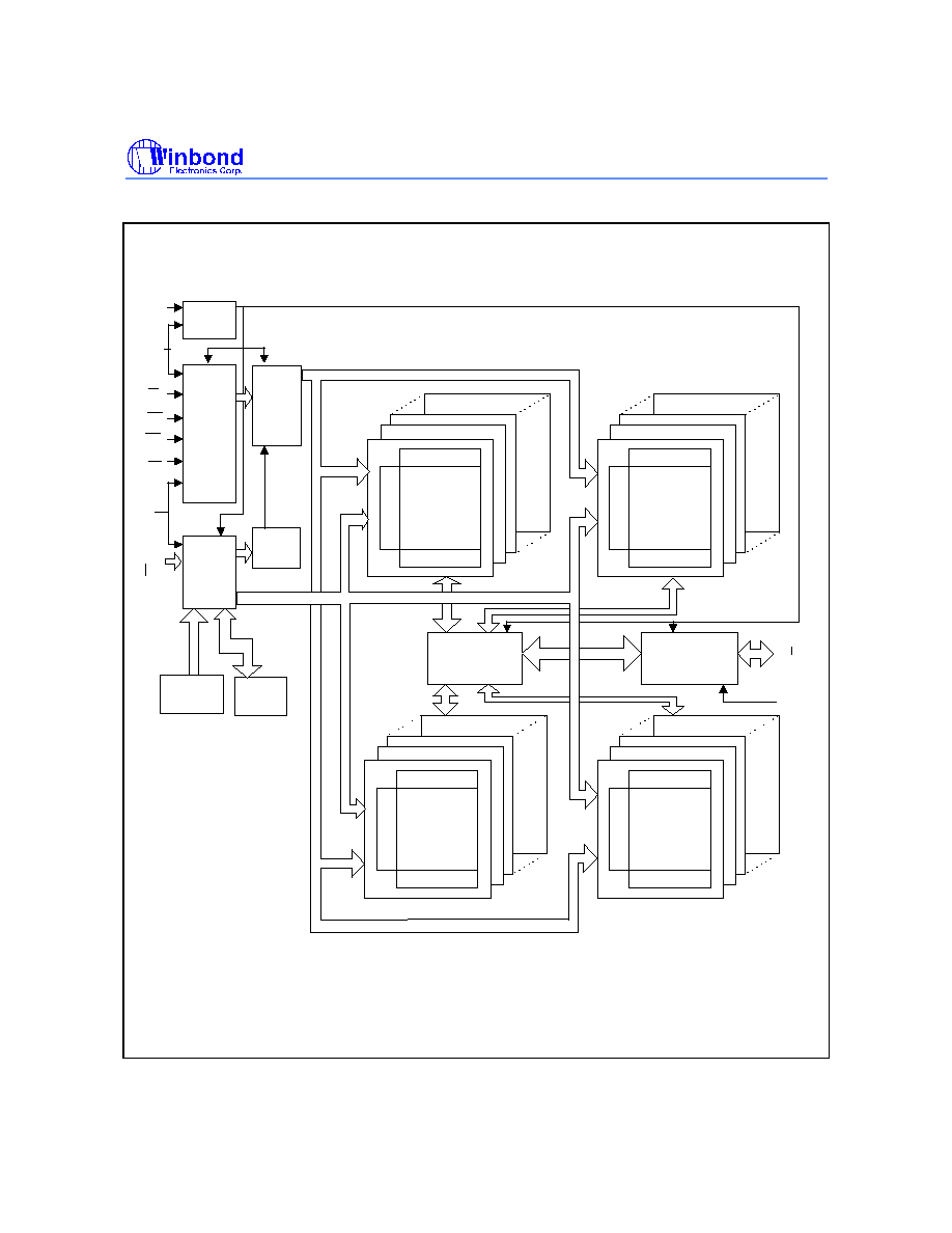
6. BLOCK DIAGRAM
D Q 0
DQ15
U D Q M
L D Q M
C L K
C K E
C S
R A S
C A S
W E
A 1 0
A 0
A 9
A 1 1
B S 0
B S 1
C L O C K
B U F F E R
C O M M A N D
D E C O D E R
A D D R E S S
B U F F E R
R E F R E S H
C O U N T E R
C O L U M N
C O U N T E R
C O N T R O L
SIGNAL
G E N E R A T O R
M O D E
R E G ISTER
C O L U M N D E C O D E R
S E N S E A M P L IFIER
CELL ARRAY
BANK #2
C O L U M N D E C O D E R
S E N S E A M P L IFIER
CELL ARRAY
BANK #0
C O L U M N D E C O D E R
S E N S E A M P L IFIER
CELL ARRAY
BANK #3
D A T A C O N T R O L
CIRCUIT
D Q
BUFFER
C O L U M N D E C O D E R
S E N S E A M P L IFIER
CELL ARRAY
BANK #1
Note: The cell array configuration is 4096 * 512 * 16.
D M n
R
O
W
D
E
C
O
D
E
R
R
O
W
D
E
C
O
D
E
R
R
O
W
D
E
C
O
D
E
R
R
O
W
D
E
C
O
D
E
R
Preliminary W987Y6CB
Publication Release Date: May 21, 2002
- 7 - Revision A1
7. ABSOLUTE MAXIMUM RATINGS
PARAMETER
SYMBOL
RATING
UNIT
NOTE
Input/Output Voltage
V
IN
, V
OUT
-0.3
-
V
DD
+0.3
V
1
Power Supply Voltage
V
DD
, V
DDQ
-0.3
-
3.6
V
1
Operating Temperature (Commercial parts)
T
OPR
0
-
70
∞
C
1
Operating Temperature (Industrial parts)
T
OPR
-40
-
85
∞
C
1
Storage Temperature
T
STG
-55
-
150
∞
C
1
Soldering Temperature (10s)
T
SOLDER
260
∞
C
1
Power Dissipation
PD
1
W
1
Short Circuit Output Current
I
OUT
50
mA
1
Note: Exposure to conditions beyond those listed under Absolute Maximum Ratings may adversely affect the life and reliability
of the device.
8. DC ELECTRICAL CHARACTERISTICS AND OPERATING CONDITIONS
(T
A
= 0
∞
C to 70
∞
C for commercial parts, T
A
= -40
∞
C to 85
∞
C for Industrial parts)
PARAMETER
SYM.
MIN.
TYP.
MAX.
UNIT
Supply Voltage
V
DD
2.3
2.5
2.7
V
Supply Voltage (for I/O Buffer)
V
DDQ
2.3
2.5
2.7
V
Input High level Voltage
V
IH
0.8*V
DDQ
-
V
DDQ
+0.3
V
Input Low level Voltage
V
IL
-0.3
-
0.2*V
DDQ
V
LVTTL Output "H" Level Voltage
(I
OUT
= -0.1 mA )
V
OH
V
DDQ
≠ 0.2
-
-
V
LVTTL Output "L" Level Voltage
(I
OUT
= +0.1 mA )
V
OL
-
-
0.2
V
Input Leakage Current
(0V
V
IN
V
DD
, all other pins not under test = 0V)
I
I(L)
-5
-
5
µ
A
Output Leakage Current
(Output disable , 0V
V
OUT
V
CCQ
)
I
O(L)
-5
-
5
µ
A
Note: V
IH
(max.) = V
DD
/ V
DDQ
+1.2V for pulse width < 5 nS
V
IL
(min.) = V
SS
/ V
SSQ
-1.2V for pulse width < 5 nS
Preliminary W987Y6CB
- 8 -
9. CAPACITANCE
(V
DD
= 2.5V, f = 1 MHz, T
A
= 25
∞
C)
PARAMETER
SYMBOL
MIN.
MAX.
UNIT
Input Capacitance
(A0 to A11, BS0, BS1,
CS
,
RAS
,
CAS
,
WE
, DQM, CKE)
CI
-
3.8
pF
Input Capacitance (CLK)
CCLK
-
3.5
pF
Input/Output Capacitance
CIO
-
6.5
pF
Note: These parameters are periodically sampled and not 100% tested.
10. OPERATING CURRENT
(V
DD
= 2.5V
±
0.2V, T
A
= 0
∞
C to 70
∞
C for commercial parts, T
A
= -40
∞
C to 85
∞
C for Industrial parts)
-75/75I
-8/-8I
PARAMETER
SYM.
MAX.
MAX.
UNIT NOTES
Operating Current
t
CK
= min., t
RC
= min.
Active precharge command cycling without
burst operation
1 bank operation
I
CC1
65
60
3
Standby Current
t
CK
= min,
CS
= V
IH
CKE = V
IH
I
CC2
15
15
3
V
IH
/
L
= V
IH
(min.)/ V
IL
(max.)
Bank: Inactive state
CKE = V
IL
(Power Down mode)
I
CC2P
0.5
0.5
3
Standby Current
CLK = V
IL
,
CS
= V
IH
CKE = V
IH
I
CC2S
10
10
V
IH
/
L
= V
IH
(min.)/ V
IL
(max.)
BANK: Inactive state
CKE = V
IL
(Power down mode)
I
CC2PS
0.35
0.35
mA
No Operating Current
t
CK
= min.,
CS
= V
IH
(min.)
CKE = V
IH
I
CC3
20
20
BANK: Active state
(4 banks)
CKE = V
IL
(Power down mode)
I
CC3P
2
2
Burst Operating Current
t
CK
= min. Read/ Write command cycling
I
CC4
90
85
3, 4
Auto Refresh Current
t
CK
= min. Auto refresh command cycling
I
CC5
150
140
3
Self Refresh Current
Self Refresh Mode CKE = 0.2V
I
CC6
400
400
µ
A
Deep Power Down Mode Current
I
CC7
10
10
µ
A
Preliminary W987Y6CB
Publication Release Date: May 21, 2002
- 9 - Revision A1
11. AC CHARACTERISTICS AND OPERATING CONDITION
(Vcc = 2.5V
±
0.2V, T
A
= 0
∞
to 70
∞
C for commercial parts ,T
A
= -40
∞
C to 85
∞
C for Industrial parts; Notes: 5, 6, 7, 8)
-75/75I
-8/-8I
PARAMETER
SYM.
MIN.
MAX.
MIN.
MAX.
UNIT
Ref/Active to Ref/Active Command Period
t
RC
65
68
Active to precharge Command Period
t
RAS
45
100000
48
100000
nS
Active to Read/Write Command Delay Time
t
RCD
20
20
Read/Write(a) to Read/Write(b)Command Period
t
CCD
1
1
Cycle
Precharge to Active Command Period
t
RP
20
20
Active(a) to Active(b) Command Period
t
RRD
15
16
Write Recovery Time
CL* = 2
10
10
CL* = 3
t
WR
7.5
8
CLK Cycle Time
CL* = 2
10
10
CL* = 3
t
CK
7.5
8
CLK High Level width
t
CH
2.5
3
CLK Low Level width
t
CL
2.5
3
Access Time from CLK
CL* = 2
6
6
CL* = 3
t
AC
5.4
6
nS
Output Data Hold Time
t
OH
3
3
Output Data High Impedance Time
t
HZ
3
7.5
3
8
Output Data Low Impedance Time
t
LZ
0
0
Power Down Mode Entry Time
t
SB
0
7.5
0
8
Transition Time of CLK
(Rise and Fall)
t
T
0.3
10
0.3
10
Data-in Set-up Time
t
DS
1.5
2
Data-in Hold Time
t
DH
1
1
Address Set-up Time
t
AS
1.5
2
Address Hold Time
t
AH
1
1
CKE Set-up Time
t
CKS
1.5
2
CKE Hold Time
t
CKH
1
1
Command Set-up Time
t
CMS
1.5
2
Command Hold Time
t
CMH
1
1
Refresh Time
t
REF
64
64
mS
Mode Register Set Cycle Time
t
RSC
15
16
nS
*CL = CAS Latency
Preliminary W987Y6CB
- 10 -
Notes:
1. Operation exceeds "ABSOLUTE MAXIMUM RATING" may adversely affect the life and reliability of
the devices.
2. All voltages are referenced to V
SS
3. These parameters depend on the cycle rate and listed values are measured at a cycle rate with the
minimum values of t
CK
and t
RC
.
4. These parameters depend on the output loading conditions. specified values are obtained with
output open.
5. Power up sequence is further described in the "Functional Description" section.
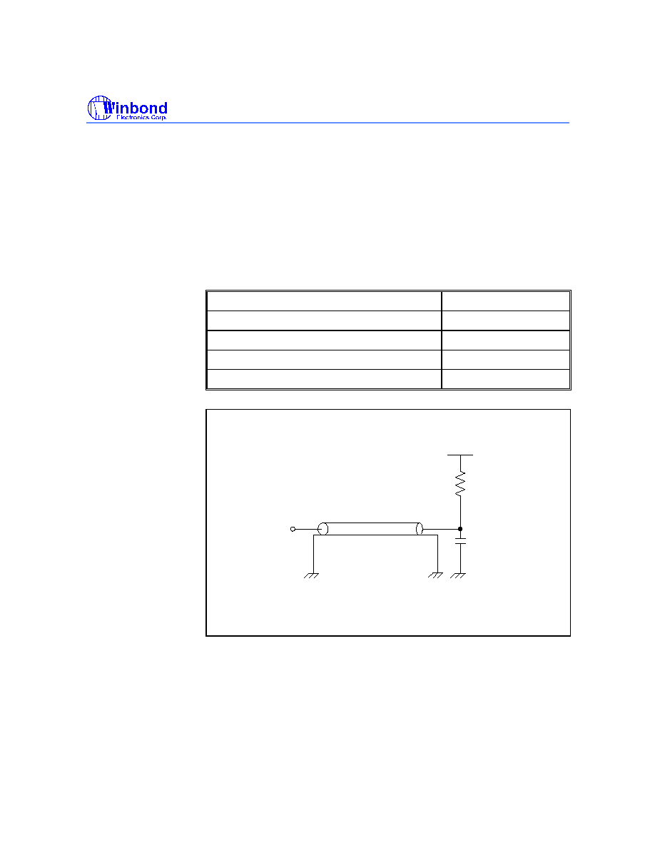
6. AC Testing Conditions
Output Reference Level
0.5 * V
DDQ
Output Load
See diagram below
Input Signal Levels
0.8* V
DDQ
/ 0.2* V
DDQ
Transition Time (Rise and Fall) of Input Signal
1 nS
Input Reference Level
0.5 * V
DDQ
50 ohms
AC TEST LOAD
Z = 50 ohms
output
30pF
0.5 x V
DD
Q
7. Transition times are measured between V
IH
and V
IL
.
8. t
HZ
defines the time at which the outputs achieve the open circuit condition and is not referenced to
output level.
9. The value that shown on table are based on silicon simulation result. It will be changed according
to real product characteristic.
Preliminary W987Y6CB
Publication Release Date: May 21, 2002
- 11 - Revision A1
Operation Mode
Fully synchronous operations are performed to latch the commands at the positive edges of CLK.
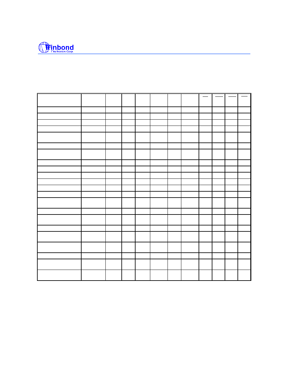
Table 1 shows the truth table for the operation commands.
Table 1 Truth Table (Note (1), (2))
COMMAND
DEVICE
STATE
CKEn-1 CKEn
DQM BS0, 1 A10
A0
-
A9
A11
CS RAS
CAS
WE
Bank Active
Idle
H
x
x
v
v
v
L
L
H
H
Bank Precharge
Any
H
x
x
v
L
x
L
L
H
L
Precharge All
Any
H
x
x
x
H
x
L
L
H
L
Write
Active (3)
H
x
x
v
L
v
L
H
L
L
Write with
Autoprecharge
Active (3)
H
x
x
v
H
v
L
H
L
L
Read
Active (3)
H
x
x
v
L
v
L
H
L
H
Read with
Autoprecharge
Active (3)
H
x
x
v
H
v
L
H
L
H
Mode Register Set
Idle
H
x
x
v
v
v
L
L
L
L
No - Operation
Any
H
x
x
x
x
x
L
H
H
H
Burst Stop
Active (4)
H
x
x
x
x
x
L
H
H
L
Device Deselect
Any
H
x
x
x
x
x
H
x
x
x
Auto - Refresh
Idle
H
H
x
x
x
x
L
L
L
H
Self - Refresh Entry
Idle
H
L
x
x
x
x
L
L
L
H
Self Refresh Exit
idle
(S.R.)
L
L
H
H
x
x
x
x
x
x
x
x
H
L
x
H
x
H
x
x
Clock Suspend Entry
Active
H
L
x
x
x
x
x
x
x
x
Power Down Entry
Idle
Active (5)
H
H
L
L
x
x
x
x
x
x
x
x
H
L
x
H
x
H
x
x
Clock Suspend Exit
Active
L
H
x
x
x
x
x
x
x
x
Power Down Exit
Any
(power down)
L
L
H
H
x
x
x
x
x
x
x
x
H
L
x
H
x
H
x
x
Deep Power Down
Entry
Idle
H
L
x
x
x
x
L
H
H
L
Deep Power Down Exit
DPDM
L
H
x
x
x
x
x
x
x
x
Data write/Output
Enable
Active
H
x
L
x
x
x
x
x
x
x
Data write/Output
Disable
Active
H
x
H
x
x
x
x
x
x
x
Notes:
1. V = Valid X = Don't care L = Low Level H = High Level
2. CKEn signal is input level when commands are provided. CKEn-1 signal is the input level one clock cycle before the
command is issued.
3. These are state of bank designated by BS0, BS1 signals.
4. Device state is full page burst operation.
5. Power Down Mode can not be entered in the burst cycle. When this command asserts in the burst cycle, device state is
clock suspend mode.

Preliminary W987Y6CB
- 12 -
12. FUNCTIONAL DESCRIPTION
Power Up Sequence
The default power up state of the mode register is unspecified. The following power up and
initialization sequence need to be followed to guarantee the device being preconditioned to each user
specific needs.
During power up, all V
DD
and V
DDQ
pins must be ramp up simultaneously to the specified voltage
when the input signals are held in the "NOP" state. The power up voltage must not exceed V
DD
+0.3V
on any of the input pins or V
DD
supplies. After power up, an initial pause of 200
µ
S is required followed
by a precharge of all banks using the precharge command. To prevent data contention on the DQ bus
during power up, it is required that the DQM and CKE pins be held high during the initial pause period.
Once all banks have been precharged, the Mode Register Set Command must be issued to initialize
the Mode Register. An additional eight Auto Refresh cycles (CBR) are also required before or after
programming the Mode Register to ensure proper subsequent operation.
Command Function
Bank Activate command
( RAS = "L", CAS = "H", WE ="H", BS0, BS1 = Bank, A0 to A11 = Row Address)
The Bank Activate command activates the bank designated by the BS (Bank select) signal. Row
addresses are latched on A0 to A11 when this command is issued and the cell data is read out of
the sense amplifiers. The maximum time that each bank can be held in the active state is
specified as t
RAS (max)
. After this command is issued, Read or Write operation can be executed.
Bank Precharge command
( RAS ="L", CAS ="H", WE ="L", BS0, BS1 = Bank, A10 ="L", A0 to A9, A11 = Don't care)
The Bank Precharge command percharges the bank designated by BS. The precharged bank is
switched from the active state to the idle state.
Precharge All command
( RAS ="L", CAS ="H", WE ="L", BS0, BS1 = Don't care, A10 = "H", A0 to A9, A11 = Don't care)
The Precharge All command precharges all banks simultaneously. Then all banks are switched to
the idle state.
Write command
( RAS ="H", CAS ="L", WE ="L", BS0, BS1 = Bank, A10 ="L", A0 to A8 = Column Address)
The write command performs a Write operation to the bank designated by BS. The write data are
latched at rising edge of CLK. The length of the write data (Burst Length) and column access
sequence (Addressing Mode) must be programmed in the Mode Register at power-up prior to the
Write operation.

Preliminary W987Y6CB
Publication Release Date: May 21, 2002
- 13 - Revision A1
Write with Auto Precharge command
( RAS ="H", CAS ="L", WE ="L", BS0, BS1 = Bank, A10="H", A0 to A8 = Column Address)
The Write with Auto Precharge command performs the Precharge operation automatically after
the Write operation. This command must not be interrupted by any other commands.
Read command
( RAS ="H", CAS ="L", WE ="H", BS0, BS1 = Bank, A10 ="L", A0 to A8 = Column Address)
The Read command performs a Read operation to the bank designated by BS. The length of read
data (Burst Length), Addressing Mode and CAS Latency (access time from CAS command in a
clock cycle) must be programmed in the Mode Register at power-up prior to the Read operation.
Read with Auto Precharge command
( RAS ="H", CAS ="L", WE ="H", BS0, BS1 = Bank, A10 ="H", A0 to A8 = Column Address)
The Read with Auto precharge command automatically performs the Precharge operation after
the Read operation. This command must not be interrupted by any other command.
Mode Register Set command
( RAS ="L", CAS ="L", WE ="L", BS0 ="L", BS1 ="L", A0 to A11 = Register Data)
The Mode Register Set command programs the values of Burst Length, Addressing Mode, CAS
latency and Write Mode in the Mode Register. The default values in the Mode Register after
power-up are undefined, therefore this command must be issued during the power-up sequence.
Also, this command can be issued while all banks are in the idle state. Refer to the table for
specific codes.
Extended Mode Register Set command
( RAS ="L", CAS ="L", WE ="L", BS0 ="L", BS1 ="H", A0 to A11 = Register data)
The Extended Mode Register Set command programs the values of Driver Strength, Temperature
Compensated Self Refresh and Partial Array Self Refresh. The default value of the extended
mode register is Full Driver Strength, 70 degrees C and All banks Refreshed
No-Operation command
( RAS ="H", CAS ="H", WE ="H")
The No-Operation command simply performs no operation (same command as Device Deselect).
Burst Read stop command
( RAS ="H", CAS ="H", WE ="L")
The Burst stop command is used to stop the burst operation. This command is only valid during a
Burst Read operation.

Preliminary W987Y6CB
- 14 -
Device Deselect command
( CS ="H")
The Device Deselect command disables the command decoder so that the RAS , CAS , WE and
Address inputs are ignored. This command is similar to the No-Operation command.
Auto Refresh command
( RAS ="L", CAS ="L", WE ="H", CKE ="H", BS0, BS1, A0 to A11 = Don't care)
The Auto Refresh command is used to refresh the row address provided by the internal refresh
counter. The Refresh operation must be performed 4096 times within 64ms. The next command
can be issued after t
RC
from the end of the Auto Refresh command. When the Auto Refresh
command is used, all banks must be in the idle state.
Self Refresh Entry command
( RAS ="L", CAS ="L", WE ="H", CKE="L", BS0, BS1, A0 to A11 = don't care)
The Self Refresh Entry command is used to enter Self Refresh mode. While the device is in Self
Refresh mode, all input and output buffer (except the CKE buffer) are disabled and the Refresh
operation is automatically performed. Self Refresh mode is exited by taking CKE "high" (the Self
Refresh Exit command).
Self Refresh Exit command
(CKE = "H" during SDRAM in Self Refresh Mode)
This command is used to exit from Self Refresh mode. Any subsequent commands can be issued
after t
RC
from the end of this command.
Deep Power Down Mode Entry command
( RAS ="H", CAS ="H", WE ="L", CKE ="L", BS0, BS1, A0 to A11 = don't care)
The Deep Power Down Mode Entry command is used to enter Deep Power Down mode. While
the device is in Deep Power Down mode, all internal circuits (except the CKE buffer) are disabled
in order to 10uA current consumption.
Deep Power Down Mode Exit command
(CKE= "H" during SDRAM in Deep Power Down Mode)
This command is used to exit from Deep Power Down mode. Full initialization is required when
the device exits from Deep Power Down Mode.
Data Write Enable /Disable command
(LDQM, UDQM ="L/H")
During a Write cycle, the LDQM or UDQM signal functions as Data Mask and can control every
word of the input data. The LDQM signal controls DQ0 to DQ7 and UDQM signal controls DQ8 to
DQ15.

Preliminary W987Y6CB
Publication Release Date: May 21, 2002
- 15 - Revision A1
Read Operation
Issuing the Bank Activate command to the idle bank puts it into the active state. When the Read
command is issued after t
RCD
from the Bank Activate command, the data is read out sequentially. The
address inputs determine the starting column address for the burst. The initial read data becomes
available after CAS latency from the issuing of the Read command. The CAS latency must be set in
the Mode Register at power-up.
When the Precharge Operation is performed on a bank during a Burst Read and operation, the Burst
operation is terminated.
When the Read with Auto Precharge command is issued, the Precharge operation is performed
automatically after the Read cycle, then the bank is switched to the idle state. This command cannot
be interrupted by any other commands. Refer to the diagrams for Read operation.
Write Operation
Issuing the Write command after t
RCD
from the bank activate command. The address inputs determine
the starting column address. Data for the first burst write cycle must be applied on the DQ pins on the
same clock cycle that the Write Command is issued. The remaining data inputs must be supplied on
each subsequent rising clock edge until the burst length is completed. Data supplied to the DQ pins
after burst finishes will be ignored. The burst length of the Write data (Burst Length) and Addressing
Mode must be set in the Mode Register at power-up.
When the Precharge operation is performed in a bank during a Burst Write operation, the Burst
operation is terminated.
When the Write with Auto Precharge command is issued, the Precharge operation is performed
automatically after the Write cycle, then the bank is switched to the idle state, The Write with Auto
Precharge command cannot be interrupted by any other command for the entire burst data duration.
Precharge
The Precharge Command is used to precharge or close a bank that has been activated. The
Precharge Command is entered when CS, RAS and WE are low and CAS is high at the rising edge of
the clock. The Precharge Command can be used to precharge each bank separately or all banks
simultaneously. Three address bits, A10, BS0, and BS1, are used to define which bank(s) is to be
precharged when the command is issued. After the Precharge Command is issued, the precharged
bank must be reactivated before a new read or write access can be executed. The delay between the
Precharge Command and the Activate Command must be greater than or equal to the Precharge time
(t
RP
).
Burst Termination
When the Precharge command is used for a bank in a Burst cycle, the Burst operation is terminated.
When Burst Read cycle is interrupted by the Precharge command, read operation is disabled after
clock cycle of ( CAS latency) from the Precharge command. When the Burst Write cycle is interrupted
by the Precharge command . the input circuit is reset at the same clock cycle at which the precharge
command is issued. In this case, the DQM signal must be asserted "high" during t
WR
to prevent writing
the invalided data to the cell array.

Preliminary W987Y6CB
- 16 -
When the Burst Read Stop command is issued for the bank in a Burst Read cycle, the Burst Read
operation is terminated. The Burst read Stop command is not supported during a write burst operation.
Interruption
Read Interrupted by a Read
A Burst Read may be interrupted by another Read Command. When the previous burst is
interrupted, the remaining addresses are overridden by the new read address with the full burst
length. The data from the first Read Command continues to appear on the outputs until the CAS
latency from the interrupting Read Command the is satisfied.
Read Interrupted by a Write
To interrupt a burst read with a Write Command, DQM may be needed to place the DQs (output
drivers) in a high impedance state to avoid data contention on the DQ bus. If a Read Command
will issue data on the first and second clocks cycles of the write operation, DQM is needed to
insure the DQs are tri-stated. After that point the Write Command will have control of the DQ bus
and DQM masking is no longer needed.
Write Interrupted by a Write
A burst write may be interrupted before completion of the burst by another Write Command.
When the previous burst is interrupted, the remaining addresses are overridden by the new
address and data will be written into the device until the programmed burst length is satisfied.
Write Interrupted by a Read
A Read Command will interrupt a burst write operation on the same clock cycle that the Read
Command is activated. The DQs must be in the high impedance state at least one cycle before
the new read data appears on the outputs to avoid data contention. When the Read Command is
activated, any residual data from the burst write cycle will be ignored.
Refresh Operation
Two types of Refresh operation can be performed on the device: Auto Refresh and Self Refresh. By
repeating the Auto Refresh cycle, each bank in turn refreshed automatically. The Refresh operation
must be performed 4096 times (rows) within 64ms. The period between the Auto Refresh command
and the next command is specified by t
RC
.
The Self Refresh Mode is entered by issuing the Self Refresh Entry Command at the rising edge of
the clock. All banks must be idle prior to issuing the Self Refresh Entry Command. Once the command
is registered, CKE must be held low to keep the device in Self Refresh mode. When the SDRAM has
entered Self Refresh mode all of the external control signals, except CKE, are disabled. The clock is
internally disabled during Self Refresh Operation to save power. The device will exit Self Refresh
operation after CKE is returned high. A minimum delay time is required when the device exits Self
Refresh Operation and before the next command can be issued. This delay is equal to the t
RC
cycle
time plus the Self Refresh exit time.
If, during normal operation, AUTO REFRESH cycles are issued in bursts (as opposed to being evenly
distributed), a burst of 4,096 AUTO REFRESH cycles should be completed just prior to entering and
just after exiting the self refresh mode.
Preliminary W987Y6CB
Publication Release Date: May 21, 2002
- 17 - Revision A1
Power Down Mode
The Power Down mode is initiated by holding CKE low. All of the receiver circuits except CKE are
gated off to reduce the power. The Power Down mode does not perform any refresh operations,
therefore the device can not remain in Power Down mode longer than the Refresh period (t
REF
) of the
device.
Mode Register Set Operation
The mode register is programmed by the Mode Register Set command (MRS/EMRS) when all banks
are in the idle state. The data to be set in the Mode Register is transferred using the Address pins of
A0 to A11 inputs. The combination of BS0, BS1 detains this cycle is MRS or EMRS.
Mode Register Description
The Mode Register designates the operation mode for the read or write cycle. The register is
divided into four fields; (1) Burst Length field sets the length of burst data (2) Addressing Mode
selection bit to designate the column access sequence in a Burst cycle (3) CAS Latency field sets
the access time in clock cycle (4) Single Write Mode selection bit to designate write operation in
burst or single write.
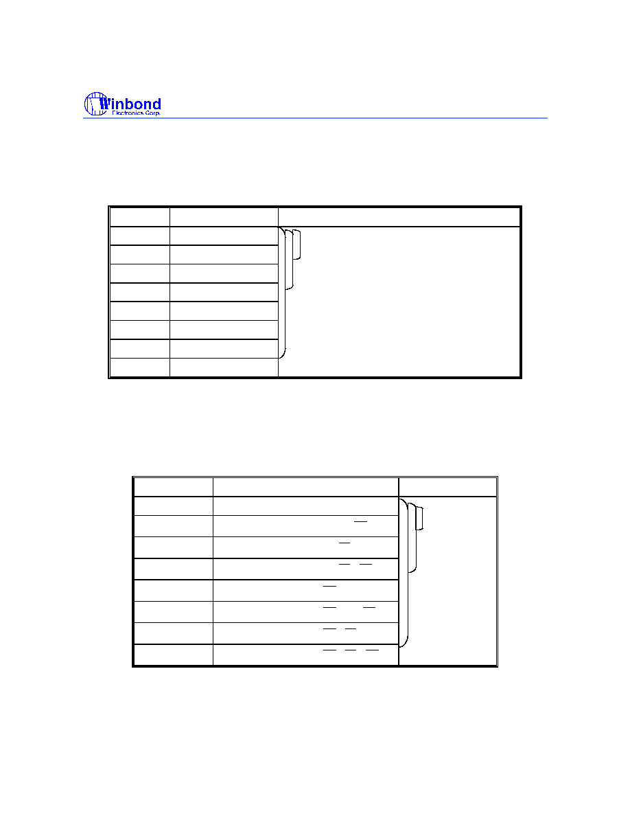
Mode Register Definition
A0
A1
A2
A3
A4
A5
A6
Burst Length
Addressing Mode
CAS Latency
(Test Mode)
A8
Reserved
A0
A7
A0
A9
A0
Write Mode
A10
A0
A11
BS0
"0"
"0"
A0
A3
A0
Addressing Mode
A0
0
A0
Sequential
A0
1
A0
Interleave
A0
A9
Single Write Mode
A0
0
A0
Burst read and Burst write
A0
1
A0
Burst read and single write
A0
A0
A2 A1 A0
A0
0 0 0
A0
0 0 1
A0
0 1 0
A0
0 1 1
A0
1 0 0
A0
1 0 1
A0
1 1 0
A0
1 1 1
A0
Burst Length
A0
Sequential
A0
Interleave
1
A0
1
A0
2
A0
2
A0
4
A0
4
A0
8
A0
8
A0
Reserved
A0
Reserved
A0
Full Page
A0
CAS Latency
A0
Reserved
A0
Reserved
2
A0
3
Reserved
A0
A6 A5 A4
A0
0 0 0
A0
0 1 0
A0
0 1 1
A0
1 0 0
A0
0 0 1
Defines it is a
MRS cycls
Reserved
"0"
"0"
BS1
"0"
"0"
Preliminary W987Y6CB
- 18 -
∑
Address sequence of Sequential mode
A column access is performed by incrementing the column address input to the device. The
address is varied by the Burst Length as the following.
Addressing Sequence of Sequential Mode
DATA
ACCESS ADDRESS
BURST LENGTH
Data 0
n
2 words (address bits is A0)
Data 1
n + 1
No carried from A0 to A1
Data 2
n + 2
4 words (address bit A0, A1)
Data 3
n + 3
Not carried from A1 to A2
Data 4
n + 4
Data 5
n + 5
8 words(address bits A2, A1 and A0)
Data 6
n + 6
Not carried from A2 to A3
Data 7
n + 7
∑
Addressing sequence of Interleave mode
A Column access is started from the inputted column address and is performed by
interleaving the address bits in the sequence shown as the following.
Address Sequence for Interleave Mode
DATA
ACCESS ADDRESS
BURST LENGTH
Data 0
A8 A7 A6 A5 A4 A3 A2 A1 A0
2 words
Data 1
A8 A7 A6 A5 A4 A3 A2 A1 A0
Data 2
A8 A7 A6 A5 A4 A3 A2 A1 A0
4 words
Data 3
A8 A7 A6 A5 A4 A3 A2 A1 A0
Data 4
A8 A7 A6 A5 A4 A3 A2 A1 A0
8 words
Data 5
A8 A7 A6 A5 A4 A3 A2 A1 A0
Data 6
A8 A7 A6 A5 A4 A3 A2 A1 A0
Data 7
A8 A7 A6 A5 A4 A3 A2 A1 A0
Preliminary W987Y6CB
Publication Release Date: May 21, 2002
- 19 - Revision A1
Simplified State Diagram
Mode
Register
Set
IDLE
CBR
Refresh
Self
Refresh
ROW
ACTIVE
Power
Down
Precharge
POWER
ON
Active
Power
Down
WRITE
WRITE
SUSPEND
WRITEA
WRITEA
SUSPEND
READ
SUSPEND
READ
READA
SUSPEND
READA
Precharge
MRS
REF
ACT
CKE
CKE
CKE
CKE
CKE
CKE
CKE
CKE
CKE
CKE
SELF
SELF exit
CKE
CKE
Write with
Read
Write
Auto precharge
Auto precharge
Read with
Write
Write
Read
PRE(precharge termination)
PRE(precharge termination)
Read
BST
BST
PRE
Manual input
Automatic sequence
Notes:
MRS = Mode Register Set
REF = Refresh
ACT = Active
PRE = Precharge
WRITEA = Write with Auto precharge
READA = Read with Auto precharge
Preliminary W987Y6CB
- 20 -
13. TIMING WAVEFORMS
Command Input Timing
CLK
A0-A11
BS0, 1
V
IH
V
IL
t
CMH
t
CMS
t
CH
t
CL
t
T
t
T
t
CKS
t
CKH
t
CKH
t
CKS
t
CKS
t
CKH
CS
RAS
CAS
WE
CKE
t
CMS
t
CMH
t
CMS
t
CMH
t
CMS
t
CMH
t
CMS
t
CMH
t
AS
t
AH
t
CK
Preliminary W987Y6CB
Publication Release Date: May 21, 2002
- 21 - Revision A1
Timing Waveforms, continued
Read Timing
Read CAS Latency
t
AC
t
LZ
t
AC
t
OH
t
HZ
t
OH
Burst Length
Read Command
CLK
CS
RAS
CAS
WE
A0-A11
BS0, 1
DQ
Valid
Data-Out
Valid
Data-Out
Preliminary W987Y6CB
- 22 -
Timing Waveforms, continued
Control Timing of Input / Output Data
t
CMH
t
CMS
t
CMH
t
CMS
t
DS
t
DH
t
DS
t
DH
t
DS
t
DH
t
DS
t
DH
Valid
Data-Out
Valid
Data-Out
Valid
Data-Out
Valid
Data-in
Valid
Data-in
Valid
Data-in
Valid
Data-in
t
CKH
t
CKS
t
CKH
t
CKS
t
DS
t
DH
t
DS
t
DH
t
DH
t
DS
t
DS
t
DH
Valid
Data-in
Valid
Data-in
Valid
Data-in
Valid
Data-in
t
CMH
t
CMS
t
CMH
t
CMS
t
OH
t
AC
t
OH
t
AC
t
OH
t
HZ
OPEN
t
LZ
t
AC
t
OH
t
AC
t
CKH
t
CKS
t
CKH
t
CKS
t
OH
t
AC
t
OH
t
AC
t
OH
t
AC
t
OH
t
AC
Valid
Data-Out
Valid
Data-Out
Valid
Data-Out
CLK
DQM
DQ0 -15
(Word Mask)
(Clock Mask)
CLK
CKE
DQ0 -15
CLK
Control Timing of Input Data
Control Timing of Output Data
(Output Enable)
(Clock Mask)
DQM
DQ0 -15
CKE
CLK
DQ0 -15
Preliminary W987Y6CB
Publication Release Date: May 21, 2002
- 23 - Revision A1
Timing Waveforms, continued
Mode Register Set Cycle
A0
A1
A2
A3
A4
A5
A6
Burst Length
Addressing Mode
CAS Latency
(Test Mode)
A8
Reserved
A0
A7
A0
A9
A0
Write Mode
A10
A0
A11
BS0
"0"
"0"
A0
A3
A0
Addressing Mode
A0
0
A0
Sequential
A0
1
A0
Interleave
A0
A9
Single Write Mode
A0
0
A0
Burst read and Burst write
A0
1
A0
Burst read and single write
A0
A0
A2 A1 A0
A0
0 0 0
A0
0 0 1
A0
0 1 0
A0
0 1 1
A0
1 0 0
A0
1 0 1
A0
1 1 0
A0
1 1 1
A0
Burst Length
A0
Sequential
A0
Interleave
1
A0
1
A0
2
A0
2
A0
4
A0
4
A0
8
A0
8
A0
Reserved
A0
Reserved
A0
Full Page
A0
CAS Latency
A0
Reserved
A0
Reserved
2
A0
3
Reserved
A0
A6 A5 A4
A0
0 0 0
A0
0 1 0
A0
0 1 1
A0
1 0 0
A0
0 0 1
t
RSC
t
CMS
t
CMH
t
CMS
t
CMH
t
CMS
t
CMH
t
CMS
t
CMH
t
AS
t
AH
CLK
CS
RAS
CAS
WE
A0-A11
BS0,1
Register
set data
next
command
A0
Reserved
"0"
"0"
BS1
"0"
"0"
Preliminary W987Y6CB
- 24 -
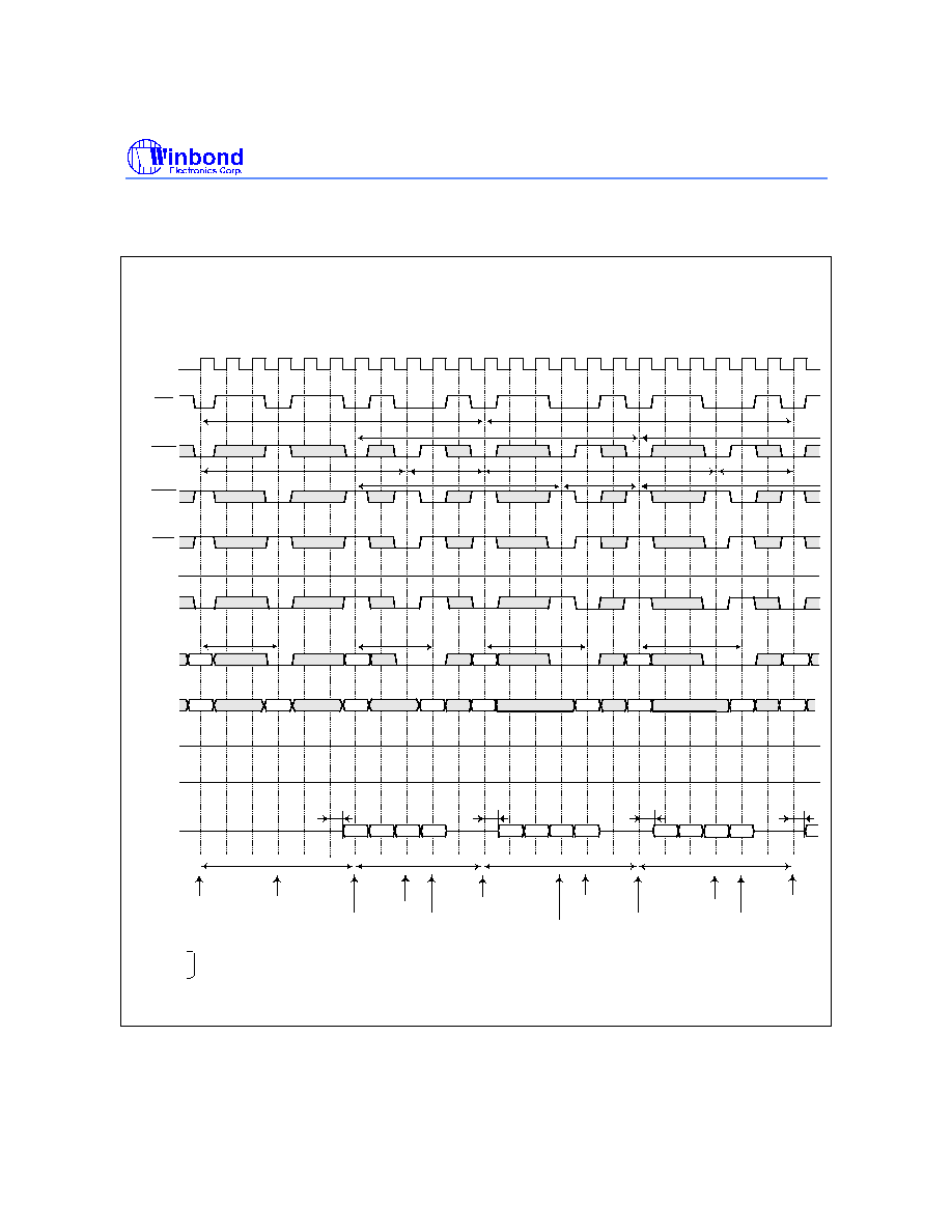
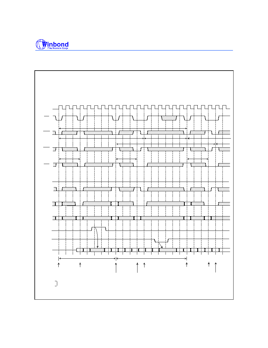
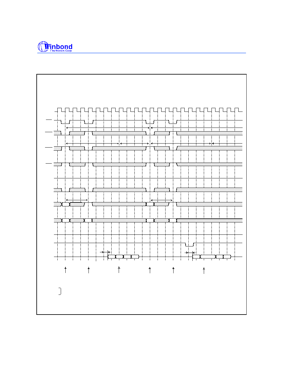
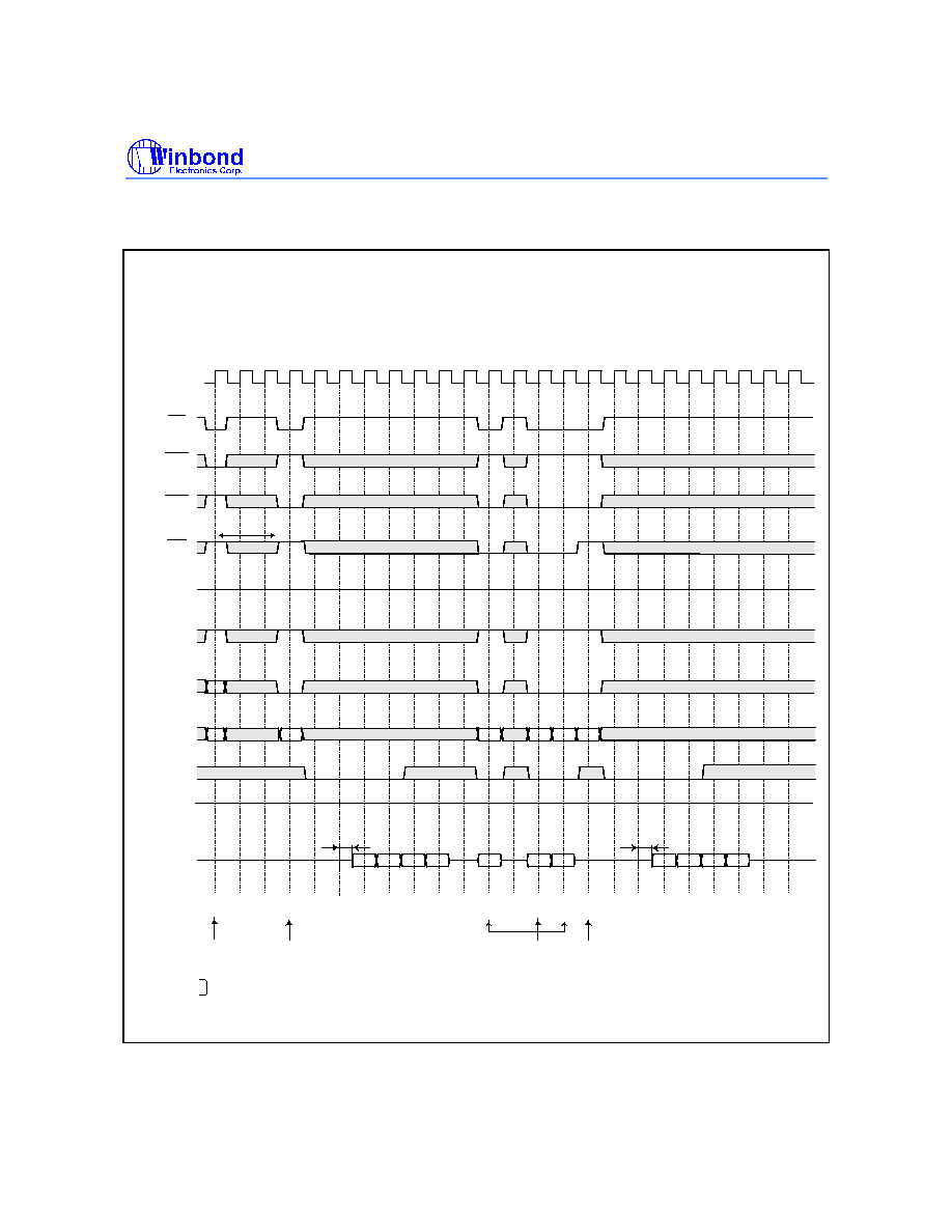
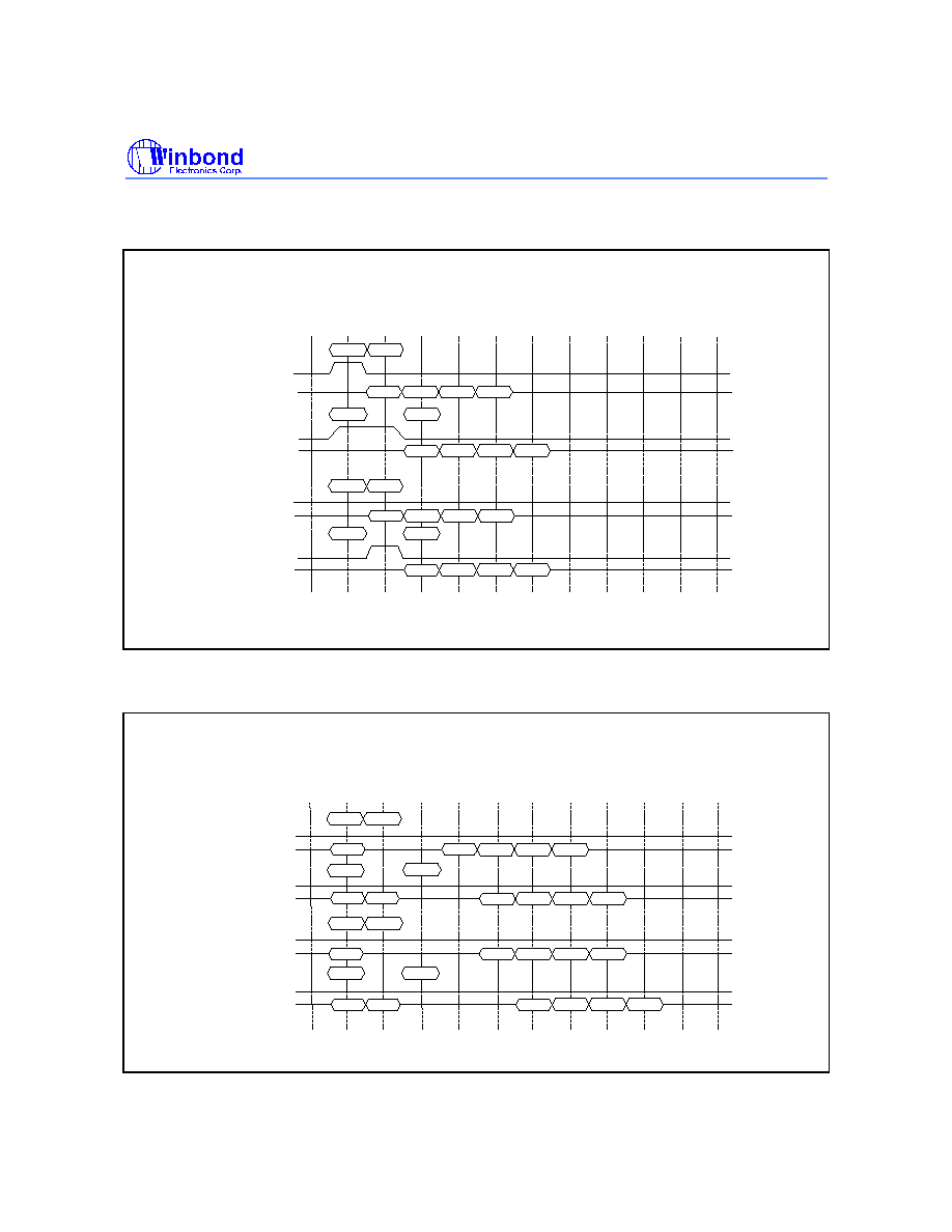
14. OPERATING TIMING EXAMPLE
Interleaved Bank Read (Burst Length = 4, CAS Latency = 3)
0
1
2
3
4
5
6
7
8
9
10
11
12
13
14
15
16
17
18
19
20
21
22
23
(CLK = 100 MHz)
CLK
DQ
CKE
DQM
A0-A9,
A11
A10
BS1
WE
CAS
RAS
CS
BS0
t
RC
t
RC
t
RC
t
RC
t
RAS
t
RP
t
RAS
t
RP
t
RP
t
RAS
t
RAS
t
RCD
t
RCD
t
RCD
t
RCD
t
AC
t
AC
t
AC
t
AC
t
RRD
t
RRD
t
RRD
t
RRD
Active
Read
Active
Read
Active
Active
Active
Read
Read
Precharge
Precharge
Precharge
RAa
RBb
RAc
RBd
RAe
RAa
CAw
RBb
CBx
RAc
CAy
RBd
CBz
RAe
aw0
aw1
aw2
aw3
bx0
bx1
bx2
bx3
cy0
cy1
cy2
cy3
Bank #0
Idle
Bank #1
Bank #2
Bank #3
Preliminary W987Y6CB
Publication Release Date: May 21, 2002
- 25 - Revision A1
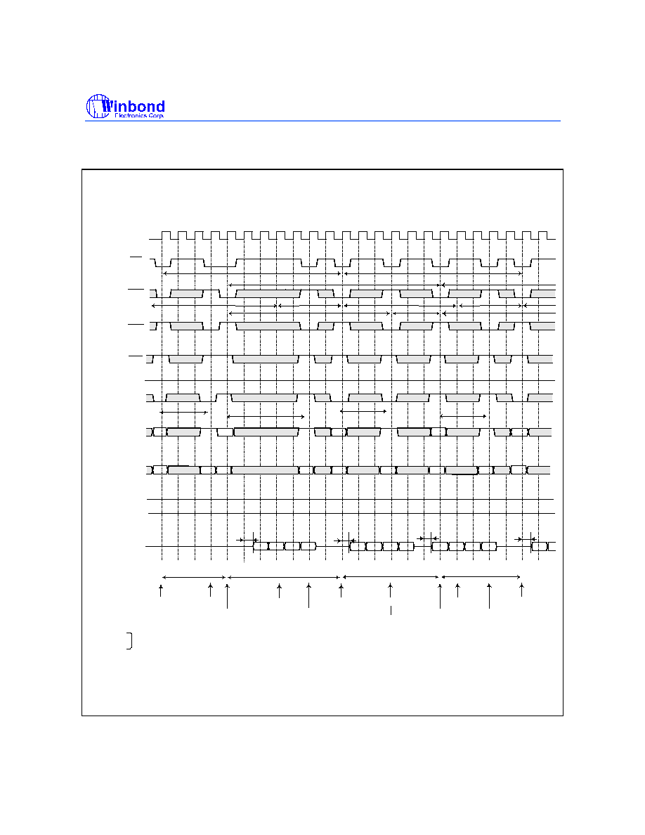
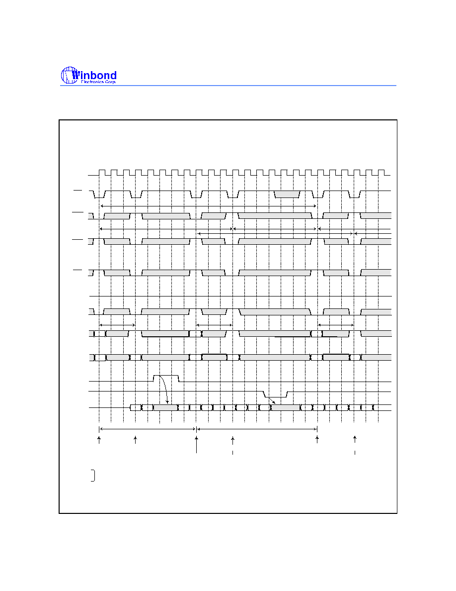
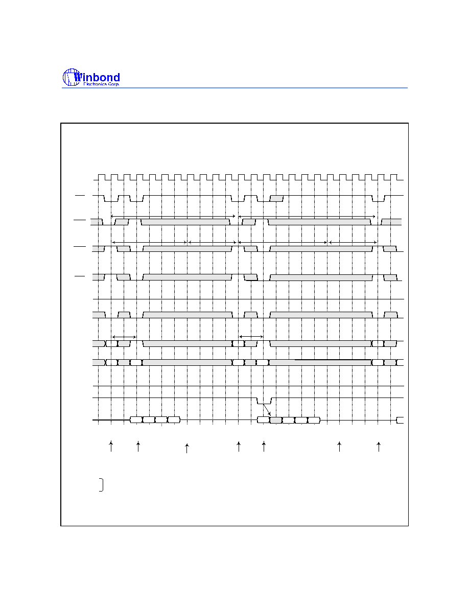
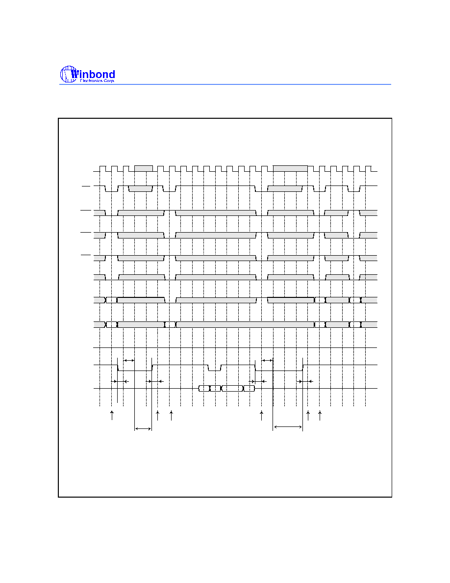
Operating Timing Example, contined
Interleaved Bank Read (Burst Length = 4, CAS Latency = 3, Autoprecharge)
0
1
2
3
4
5
6
7
8
9
10
11
12
13
14
15
16
17
18
19
20
21
22
23
(CLK = 100 MHz)
CLK
CKE
DQM
A0-A9,
A11
A10
BS1
WE
CAS
RAS
CS
BS0
t
RC
t
RC
t
RC
t
RAS
t
RP
t
RAS
t
RP
t
RAS
t
RP
t
RAS
t
RCD
t
RCD
t
RCD
t
RCD
t
AC
t
AC
t
AC
t
AC
t
RRD
t
RRD
t
RRD
t
RRD
Active
Read
Active
Read
Active
Active
Active
Read
Read
t
RC
RAa
RBb
RAc
RBd
RAe
DQ
aw0
aw1
aw2
aw3
bx0
bx1
bx2
bx3
cy0
cy1
cy2
cy3
dz0
* AP is the internal precharge start timing
Bank #0
Idle
Bank #1
Bank #2
Bank #3
AP*
AP*
AP*
RAa
CAw
RBb
CBx
RAc
CAy
RBd
RAe
CBz
Preliminary W987Y6CB
- 26 -
Operating Timing Example, contined
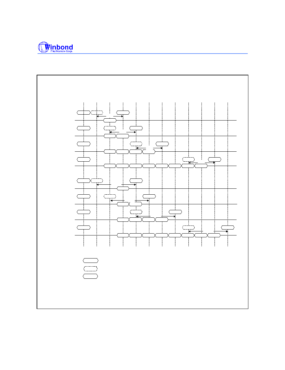
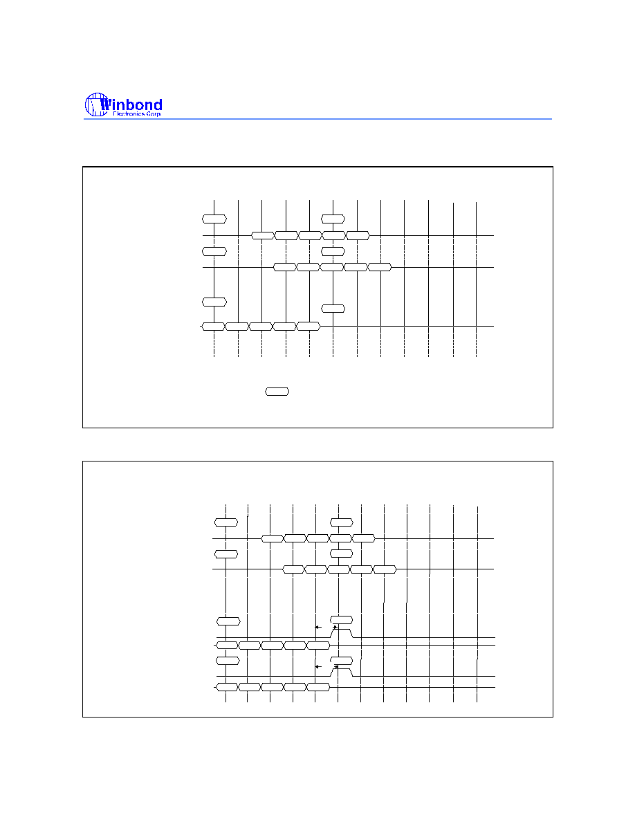
Interleaved Bank Read (Burst Length = 8, CAS Latency = 3)
0
1
2
3
4
5
6
7
8
9
10
11
12
13
14
15
16
17
18
19
20
21
22
23
t
RC
t
RC
t
RC
t
RAS
t
RP
t
RAS
t
RP
t
RAS
t
RP
t
RCD
t
RCD
t
RCD
t
RRD
t
RRD
RAa
RAa
CAx
RBb
RBb
CBy
RAc
RAc
CAz
ax0
ax1
ax2
ax3
ax4
ax5
ax6
by0
by1
by4
by5
by6
by7
CZ0
(CLK = 100 MHz)
CLK
DQ
CKE
DQM
A0-A9,
A11
A10
BS0
WE
CAS
RAS
CS
BS1
Active
Read
Precharge
Active
Read
Precharge
Active
t
AC
t
AC
Read
Precharge
t
AC
Bank #0
Idle
Bank #1
Bank #2
Bank #3
Preliminary W987Y6CB
Publication Release Date: May 21, 2002
- 27 - Revision A1
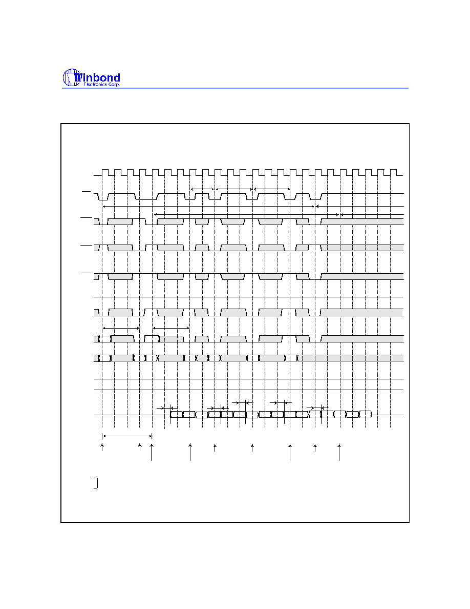
Operating Timing Example, contined
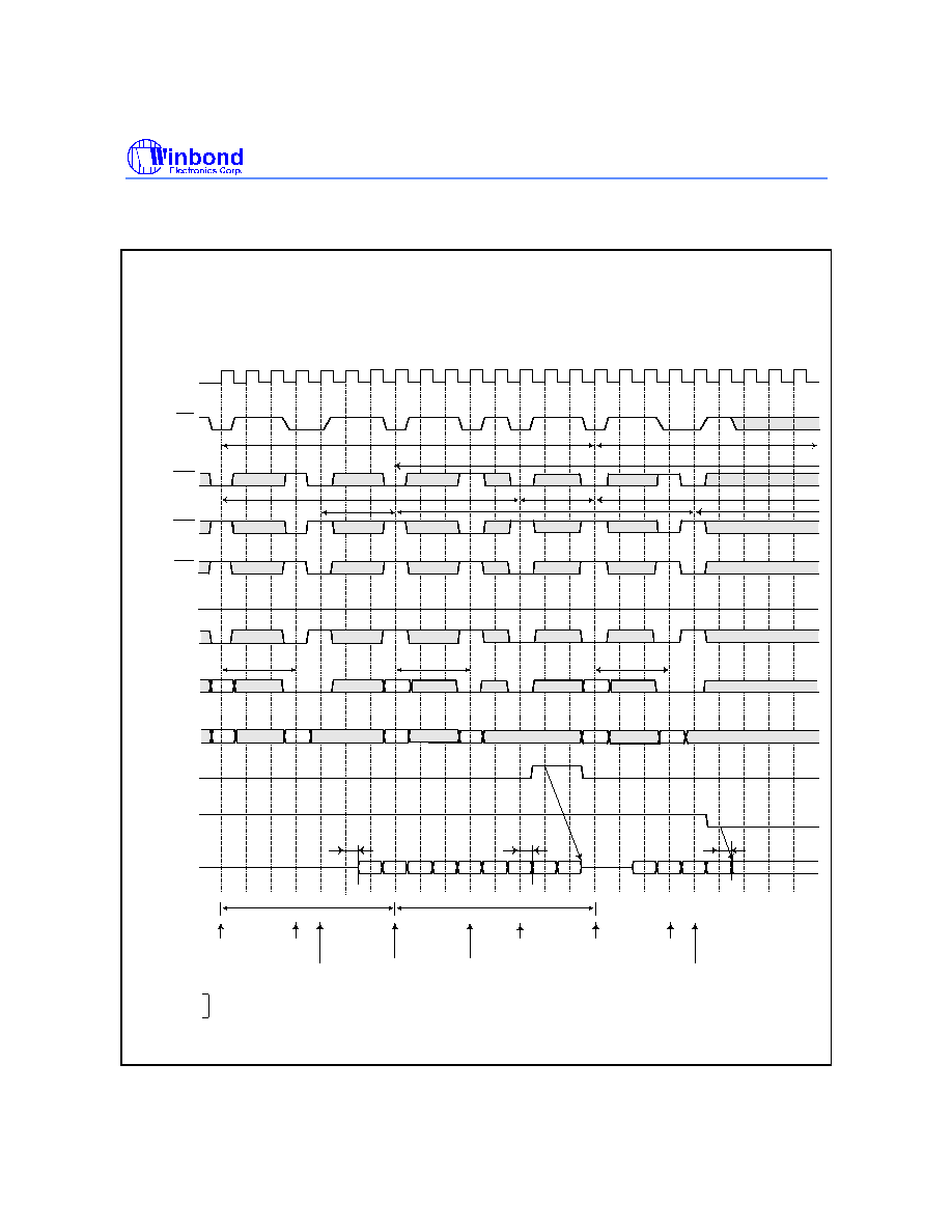
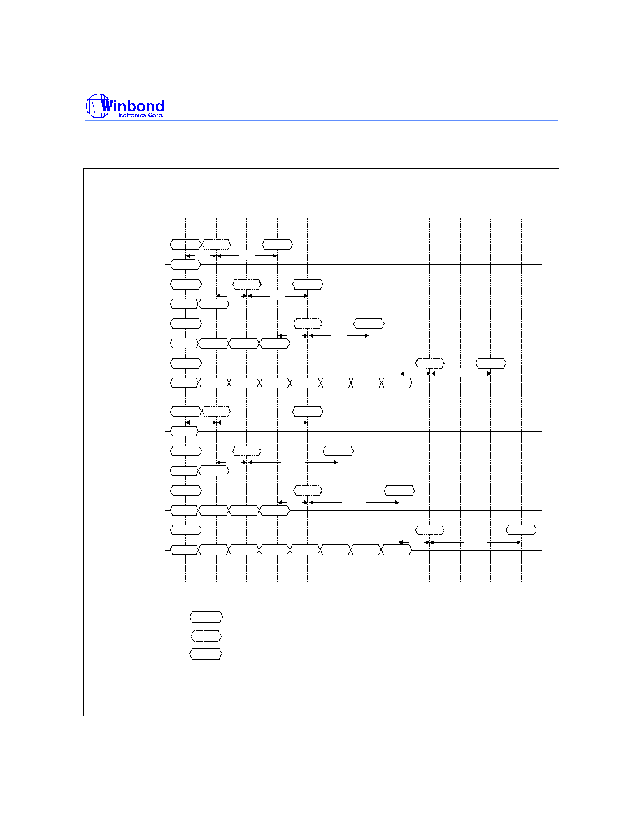
Interleaved Bank Read (Burst Length = 8, CAS Latency = 3, Autoprecharge)
0
1
2
3
4
5
6
7
8
9
10
11
12
13
14
15
16
17
18
19
20
21
22
23
t
RC
t
RC
t
RAS
t
RP
t
RAS
t
RAS
t
RP
t
RCD
t
RCD
t
RCD
t
RRD
t
RRD
ax0
ax1
ax2
ax3
ax4
ax5
ax6
ax7
by0
by1
by4
by5
by6
CZ0
RAa
RAa
CAx
RBb
RBb
CBy
(CLK = 100 MHz)
RAc
RAc
CAz
* AP is the internal precharge start timing
Active
Read
Active
Active
Read
t
CAC
t
CAC
t
CAC
CLK
DQ
CKE
DQM
A0-A9,
A11
A10
BS1
WE
CAS
RAS
CS
Bank #0
Idle
Bank #1
Bank #2
Bank #3
Read
AP*
AP*
BS0
Preliminary W987Y6CB
- 28 -
Operating Timing Example, contined
Interleaved Bank Write (Burst Length = 8)
0
1
2
3
4
5
6
7
8
9
10
11
12
13
14
15
16
17
18
19
20
21
22
23
t
RC
t
RAS
t
RP
t
RAS
t
RP
t
RCD
t
RCD
t
RCD
t
RRD
t
RRD
RAa
RAa
CAx
RBb
RBb
CBy
RAc
RAc
CAz
ax0
ax1
ax4
ax5
ax6
ax7
by0
by1
by2
by3
by4
by5
by6
by7
CZ0
CZ1
CZ2
(CLK = 100 MHz)
Write
Precharge
Active
Active
Write
Precharge
Active
Write
CLK
DQ
CKE
DQM
A0-A9,
A11
A10
BS0
WE
CAS
RAS
CS
BS1
Idle
Bank #0
Bank #1
Bank #2
Bank #3
t
RAS
Preliminary W987Y6CB
Publication Release Date: May 21, 2002
- 29 - Revision A1
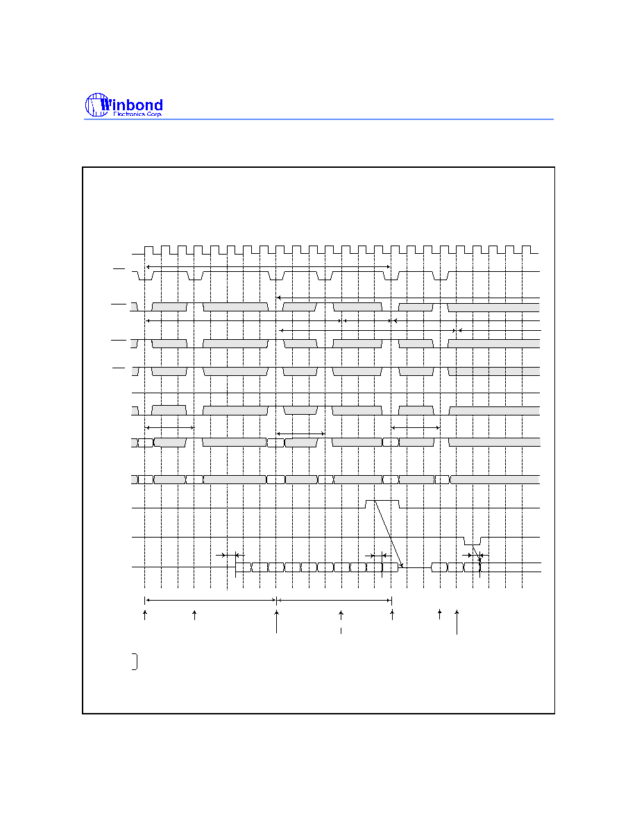
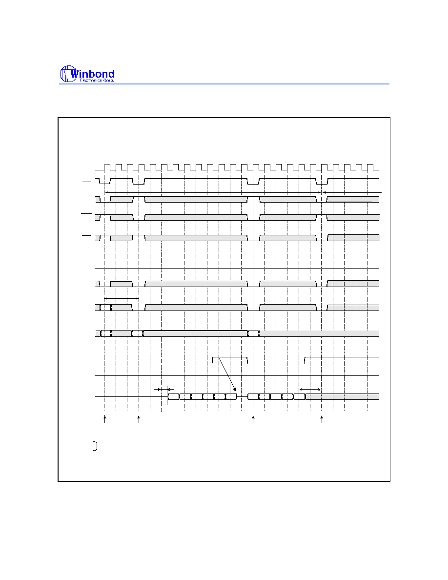
Operating Timing Example, contined
Interleaved Bank Write (Burst Length = 8, Autoprecharge)
0
1
2
3
4
5
6
7
8
9
10
11
12
13
14
15
16
17
18
19
20
21
22
23
t
RC
t
RAS
t
RP
t
RAS
t
RAS
t
RP
t
RCD
t
RCD
t
RCD
t
RRD
t
RRD
RAa
RAa
CAx
RBb
RBb
CBy
RAb
RAc
ax0
ax1
ax4
ax5
ax6
ax7
by0
by1
by2
by3
by4
by5
by6
by7
CZ0
CZ1
CZ2
CAz
(CLK = 100 MHz)
* AP is the internal precharge start timing
CLK
DQ
CKE
DQM
A0-A9,
A11
A10
BS0
WE
CAS
RAS
CS
BS1
Active
Write
Write
Active
Bank #0
Idle
Bank #1
Bank #2
Bank #3
AP*
Active
Write
AP*
Preliminary W987Y6CB
- 30 -
Operating Timing Example, contined
Page Mode Read (Burst Length = 4, CAS Latency = 3)
0
1
2
3
4
5
6
7
8
9
10
11
12
13
14
15
16
17
18
19
20
21
22
23
t
CCD
t
CCD
t
CCD
t
RAS
t
RP
t
RAS
t
RP
t
RCD
t
RCD
t
RRD
RAa
RAa
CAI
RBb
RBb
CBx
CAy
CAm
CBz
a0
a1
a2
a3
bx0
bx1
Ay0
Ay1
Ay2
am0
am1
am2
bz0
bz1
bz2
bz3
(CLK = 100 MHz)
* AP is the internal precharge start timing
CLK
DQ
CKE
DQM
A0-A9,
A11
A10
BS0
WE
CAS
RAS
CS
BS1
Active
Read
Active
Read
Read
Read
Read
Precharge
t
AC
t
AC
t
AC
t
AC
t
AC
Bank #0
Idle
Bank #1
Bank #2
Bank #3
AP*
Preliminary W987Y6CB
Publication Release Date: May 21, 2002
- 31 - Revision A1
Operating Timing Example, contined
Page Mode Read / Write (Burst Length = 8, CAS Latency = 3)
0
1
2
3
4
5
6
7
8
9
10
11
12
13
14
15
16
17
18
19
20
21
22
23
t
RAS
t
RP
t
RCD
t
WR
RAa
RAa
CAx
CAy
ax0
ax1
ax2
ax3
ax4
ax5
ay1
ay0
ay2
ay4
ay3
Q Q
Q
Q
Q
Q
D
D
D
D
D
(CLK = 100 MHz)
CLK
DQ
CKE
DQM
A0-A9,
A11
A10
BS0
WE
CAS
RAS
CS
BS1
Active
Read
Write
Precharge
t
AC
Bank #0
Idle
Bank #1
Bank #2
Bank #3
Preliminary W987Y6CB
- 32 -
Operating Timing Example, contined
Auto Precharge Read (Burst Length = 4, CAS Latency = 3)
0
1
2
3
4
5
6
7
8
9
10
11
12
13
14
15
16
17
18
19
20
21
22
23
(CLK = 100 MHz)
CLK
DQ
CKE
DQM
A0-A9,
A11
A10
BS1
WE
CAS
RAS
CS
BS0
t
RC
t
RC
t
RAS
t
RP
t
RAS
t
RP
t
RCD
t
RCD
t
AC
Active
Read
AP*
Active
Read
RAa
RAb
RAa
CAw
RAb
CAx
aw0
aw1
aw2
aw3
* AP is the internal precharge start timing
Bank #0
Idle
Bank #1
Bank #2
Bank #3
t
AC
AP*
bx0
bx1
bx2
bx3
Preliminary W987Y6CB
Publication Release Date: May 21, 2002
- 33 - Revision A1
Operating Timing Example, contined
Auto Precharge Write (Burst Length = 4)
0
1
2
3
4
5
6
7
8
9
10
11
12
13
14
15
16
17
18
19
20
21
22
23
(CLK = 100 MHz)
CLK
DQ
CKE
DQM
A0-A9,
A11
A10
BS1
WE
CAS
RAS
CS
BS0
t
RC
t
RC
t
RAS
t
RP
t
RAS
t
RP
RAa
t
RCD
t
RCD
RAb
RAc
RAa
CAw
RAb
CAx
RAc
aw0
aw1
aw2
aw3
bx0
bx1
bx2
bx3
Active
Active
Write
AP*
Active
Write
AP*
* AP is the internal precharge start timing
Bank #0
Idle
Bank #1
Bank #2
Bank #3
Preliminary W987Y6CB
- 34 -
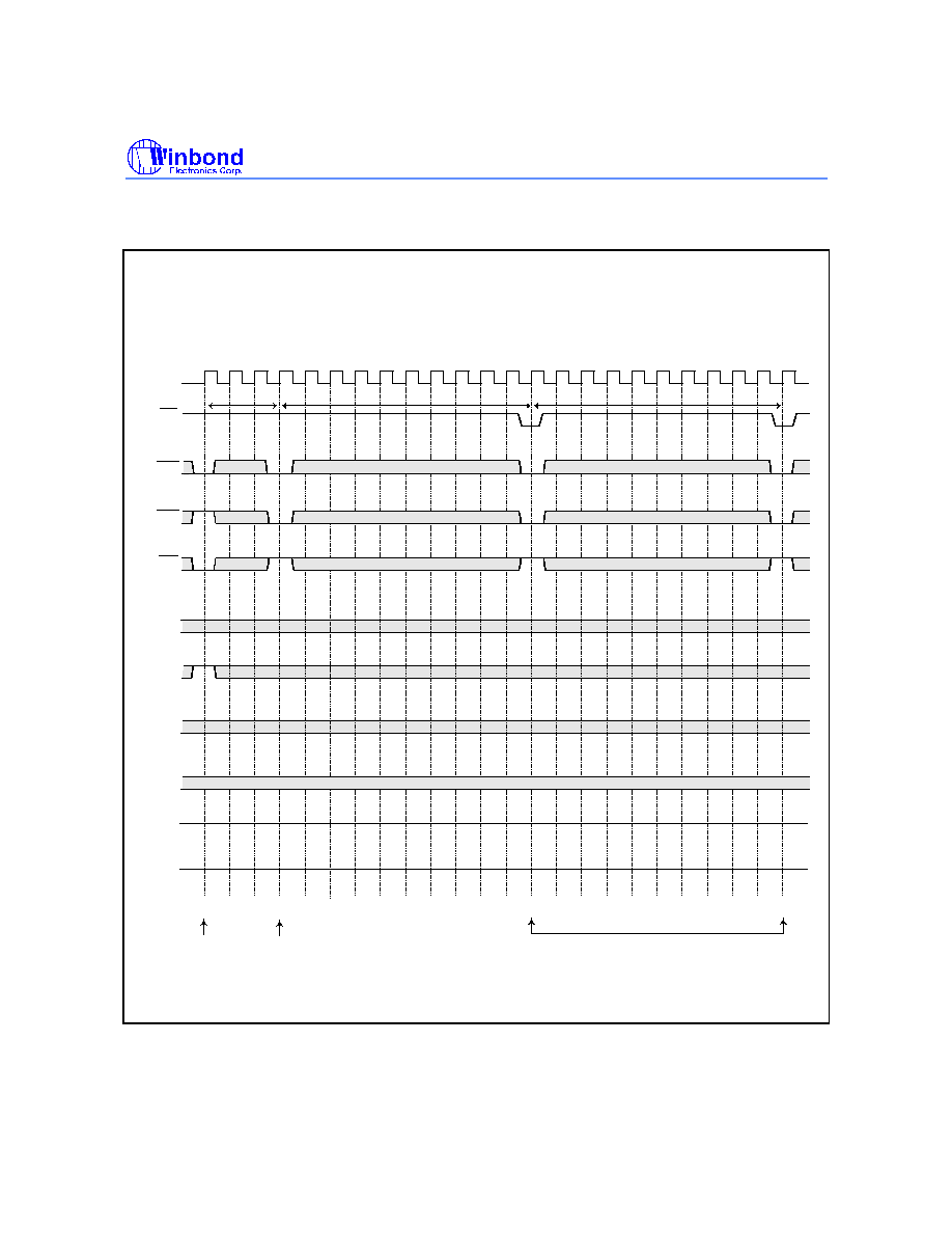
Operating Timing Example, contined
Auto Refresh Cycle
0
1
2
3
4
5
6
7
8
9
10
11
12
13
14
15
16
17
18
19
20
21
22
23
(CLK = 100 MHz)
All Banks
Prechage
Auto
Refresh
Auto Refresh (Arbitrary Cycle)
t
RC
t
RP
t
RC
CLK
DQ
CKE
DQM
A0-A9,
A11
A10
WE
CAS
RAS
CS
BS0,1
Preliminary W987Y6CB
Publication Release Date: May 21, 2002
- 35 - Revision A1
Operating Timing Example, contined
Self Refresh Cycle
0
1
2
3
4
5
6
7
8
9
10
11
12
13
14
15
16
17
18
19
20
21
22
23
(CLK = 100 MHz)
CLK
DQ
CKE
DQM
A0-A9,
A11
A10
BS0,1
WE
CAS
RAS
CS
t
CKS
t
SB
t
CKS
t
CKS
All Banks
Precharge
Self Refresh
Entry
Arbitrary Cycle
t
RP
Self Refresh Cycle
t
RC
No Operation Cycle
Preliminary W987Y6CB
- 36 -
Operating Timing Example, contined
Burst Read and Single Write (Burst Length = 4, CAS Latency = 3)
0
1
2
3
4
5
6
7
8
9
10
11
12
13
14
15
16
17
18
19
20
21
22
23
CLK
CS
RAS
CAS
WE
BS0
BS1
A10
A0-A9,
A11
DQM
CKE
DQ
(CLK = 100 MHz)
t
RCD
RBa
RBa
CBv
CBw
CBx
CBy
CBz
av0
av1
av2
av3
aw0
ax0
ay0
az0
az1
az2
az3
Q
Q
Q
Q
D
D
D
Q
Q
Q
Q
t
AC
t
AC
Read
Read
Single Write
Active
Bank #0
Idle
Bank #1
Bank #2
Bank #3
Preliminary W987Y6CB
Publication Release Date: May 21, 2002
- 37 - Revision A1
Operating Timing Example, contined
PowerDown Mode
0
1
2
3
4
5
6
7
8
9
10
11
12
13
14
15
16
17
18
19
20
21
22
23
(CLK = 100 MHz)
RAa
CAa
RAa
CAx
RAa
RAa
ax0
ax1
ax2
ax3
t
SB
t
CKS
t
CKS
t
CKS
t
SB
t
CKS
Active Standby
Power Down mode
Precharge Standby
Power Down mode
Active
NOP
Precharge
NOPActive
Note: The PowerDown Mode is entered by asserting CKE "low".
All Input/Output buffers (except CKE buffers) are turned off in the PowerDown mode.
When CKE goes high, command input must be No operation at next CLK rising edge.
CLK
DQ
CKE
DQM
A0-A9
A11
A10
BS
WE
CAS
RAS
CS
Read
Preliminary W987Y6CB
- 38 -
Operating Timing Example, contined
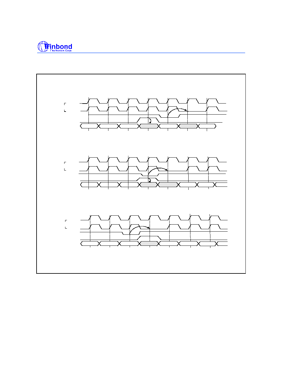
Autoprecharge Timing (Read Cycle)
Read
AP
0
11
10
9
8
7
6
5
4
3
2
1
Q0
Q0
Read
AP
Act
Q1
Read
AP
Act
Q1
Q2
AP
Act
Read
Act
Q0
Q3
(1) CAS Latency=2
Read
Act
AP
When the Auto precharge command is asserted, the period from Bank Activate command to
the start of internal precgarging must be at least t
RAS
(min).
represents the Read with Auto precharge command.
represents the start of internal precharging.
represents the Bank Activate command.
Note )
t
RP
t
RP
t
RP
( a ) burst length = 1
Command
( b ) burst length = 2
Command
( c ) burst length = 4
Command
( d ) burst length = 8
Command
DQ
DQ
DQ
DQ
Q0
Q1
Q2
Q3
Q4
Q5
Q6
Q7
t
RP
( a ) burst length = 1
Command
( b ) burst length = 2
Command
( c ) burst length = 4
Command
( d ) burst length = 8
Command
DQ
DQ
DQ
DQ
Q0
Read
AP
Act
Q0
Read
AP
Act
Q1
Q0
Read
AP
Act
Q1
Q2
Q3
Read
AP
Act
Q0
Q1
Q2
Q3
Q4
Q5
Q6
Q7
(2) CAS Latency=3
t
RP
t
RP
t
RP
t
RP
Preliminary W987Y6CB
Publication Release Date: May 21, 2002
- 39 - Revision A1
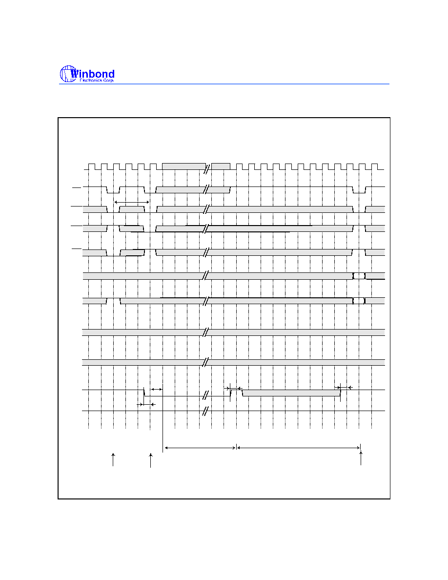
Operating Timing Example, contined
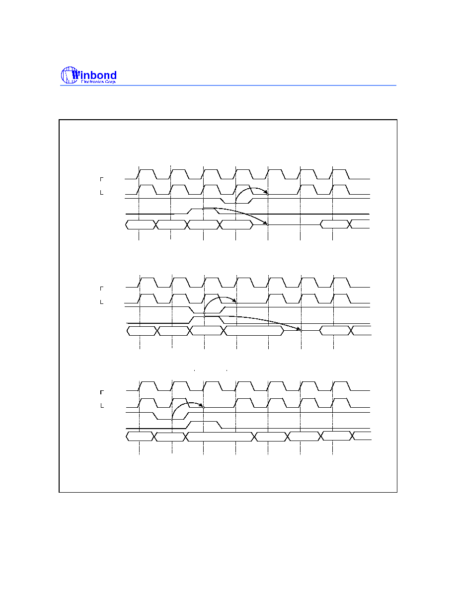
Autoprecharge Timing (Write Cycle)
Write
Act
AP
0
11
10
9
8
7
6
5
4
3
2
1
D0
D0
D0
D0
AP
Act
D1
AP
Act
D1
D1
D2
D2
D3
D3
D4
D5
D6
D7
AP
Act
Write
Write
Write
(1) CAS Latency=2
Write
Act
AP
When the Auto precharge command is asserted, the period from Bank Activate
command to the start of internal precgarging must be at least tRAS (min).
represents the Write with Auto precharge command.
represents the start of internal precharging.
represents the Bank Activate command.
Note )
t
RP
t
WR
t
RP
t
WR
t
RP
t
WR
t
RP
t
WR
( a ) burst length = 1
Command
( b ) burst length = 2
Command
( c ) burst length = 4
Command
( d ) burst length = 8
Command
DQ
DQ
DQ
DQ
D0
AP
Act
AP
Act
D1
D0
AP
Act
D1
D2
D3
AP
Act
D0
D1
D2
D3
D4
D5
D6
D7
Write
Write
Write
Write
D0
(2) CAS Latency=3
t
RP
t
WR
t
RP
t
WR
t
RP
t
WR
t
RP
t
WR
( a ) burst length = 1
Command
( b ) burst length = 2
Command
( c ) burst length = 4
Command
( d ) burst length = 8
Command
DQ
DQ
DQ
DQ
Preliminary W987Y6CB
- 40 -
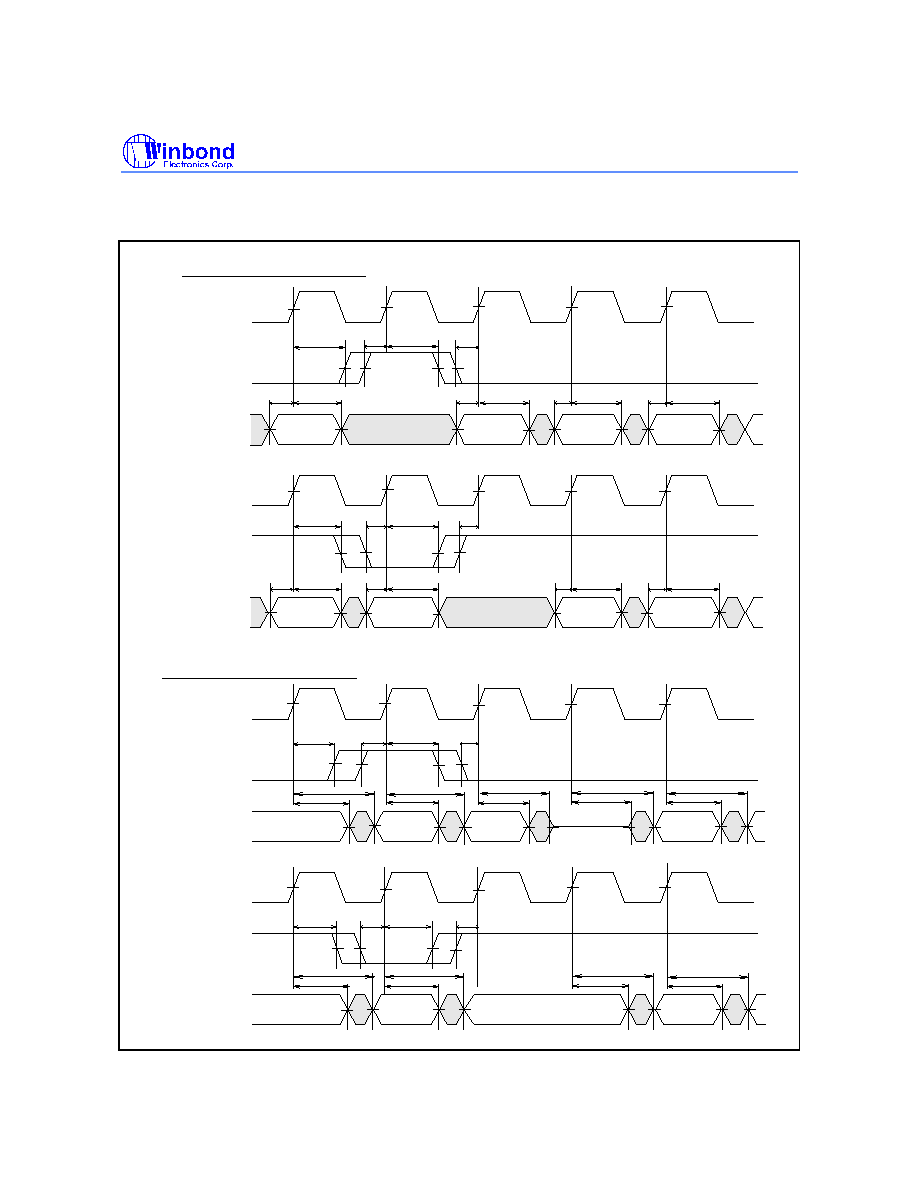
Operating Timing Example, contined
Timing Chart of Read to Write Cycle
Note: The Output data must be masked by DQM to avoid I/O conflict
11
10
9
8
7
6
5
4
3
2
1
0
(1) CAS Latency=2
In the case of Burst Length = 4
Read
Read
Write
Write
DQ
DQ
( b ) Command
DQM
DQM
D0
D1
D2
D3
D0
D1
D2
D3
( a ) Command
(2) CAS Latency=3
Read
Write
Read
Write
D0
D1
D2
D3
( a ) Command
DQ
DQ
DQM
( b ) Command
DQM
D0
D1
D2
D3
Timing Chart of Write to Read Cycle
Read
Write
0
11
10
9
8
7
6
5
4
3
2
1
Q0
Read
Q1
Q2
Q3
Read
Read
Write
Write
Q0
Q1
Q2
Q3
Write
Q0
Q1
Q2
Q3
D0
D1
DQ
DQ
( a ) Command
DQ
DQ
DQM
( b ) Command
DQM
( a ) Command
( b ) Command
DQM
DQM
In the case of Burst Length=4
(1) CAS Latency=2
(2) CAS Latency=3
D0
D0
D1
Q0
Q1
Q2
Q3
D0
Preliminary W987Y6CB
Publication Release Date: May 21, 2002
- 41 - Revision A1
Operating Timing Example, contined
Timing Chart of Burst Stop Cycle (Burst Stop Command)
Read
BST
0
11
10
9
8
7
6
5
4
3
2
1
DQ
Q0
Q1
Q2
Q3
BST
( a ) CAS latency =2
Command
( b )CAS latency = 3
(1) Read cycle
Q4
(2) Write cycle
Command
Read
Command
Q0
Q1
Q2
Q3
Q4
Q0
Q1
Q2
Q3
Q4
DQ
DQ
Write
BST
Note: represents the Burst stop command
BST
Timing Chart of Burst Stop Cycle (Precharge Command)
In the case of Burst Lenght = 8
Read
PRCG
0
11
10
9
8
7
6
5
4
3
2
1
Q0
Q1
Q2
Q3
Q0
Q1
Q2
Q3
Read
PRCG
Q4
Q4
( a )CAS latency =2
Command
( b )CAS latency = 3
Command
DQ
DQ
DQ
( b )CAS latency = 3
Command
(1) Read cycle
(2) Write cycle
Write
Write
PRCG
PRCG
( a ) CAS latency =2
Command
DQM
DQM
t
WR
t
WR
D0
D1
D2
D3
D4
DQ
D0
D1
D2
D3
D4
DQ
Preliminary W987Y6CB
- 42 -
Operating Timing Example, contined
CKE/DQM Input Timing (Write Cycle)
7
6
5
4
3
2
1
CKE MASK
( 1 )
D1
D6
D5
D3
D2
CLK cycle No.
External
Internal
CKE
DQM
DQ
7
6
5
4
3
2
1
( 2 )
D1
D6
D5
D3
D2
CLK cycle No.
External
Internal
CKE
DQM
DQ
7
6
5
4
3
2
1
( 3 )
D1
D6
D5
D4
D3
D2
CLK cycle No.
External
CKE
DQM
DQ
DQM MASK
DQM MASK
CKE MASK
CKE MASK
Internal
CLK
CLK
CLK
Preliminary W987Y6CB
Publication Release Date: May 21, 2002
- 43 - Revision A1
Operating Timing Example, contined
CKE/DQM Input Timing (Read Cycle)
7
6
5
4
3
2
1
( 1 )
Q1
Q6
Q4
Q3
Q2
CLK cycle No.
External
Internal
CKE
DQM
DQ
Open
Open
7
6
5
4
3
2
1
Q1
Q6
Q3
Q2
CLK cycle No.
External
Internal
CKE
DQM
DQ
Open
( 2 )
7
6
5
4
3
2
1
Q1
Q6
Q2
CLK cycle No.
External
Internal
CKE
DQM
DQ
Q5
Q4
( 3 )
Q4
CLK
CLK
CLK
Q3
Preliminary W987Y6CB
- 44 -
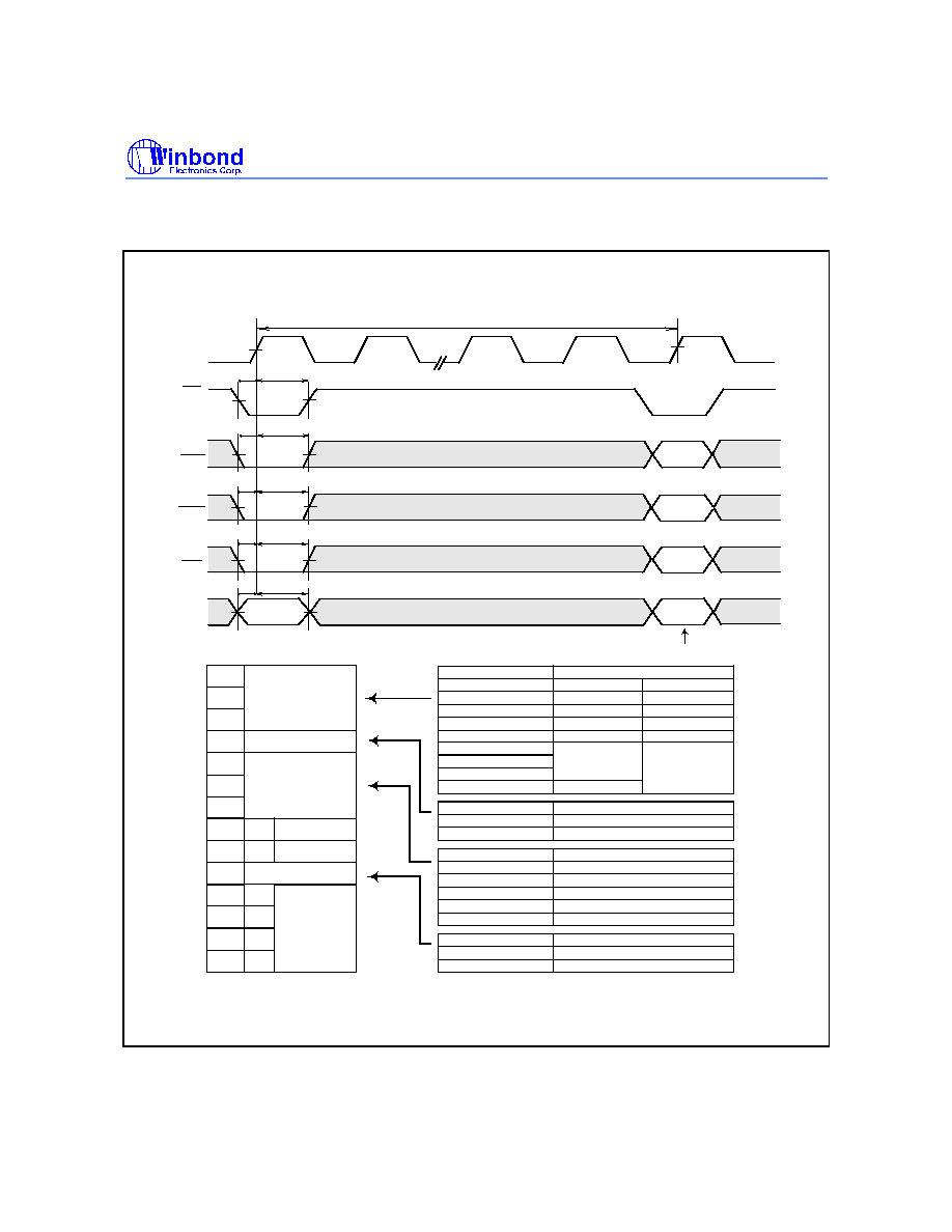
Operating Timing Example, contined
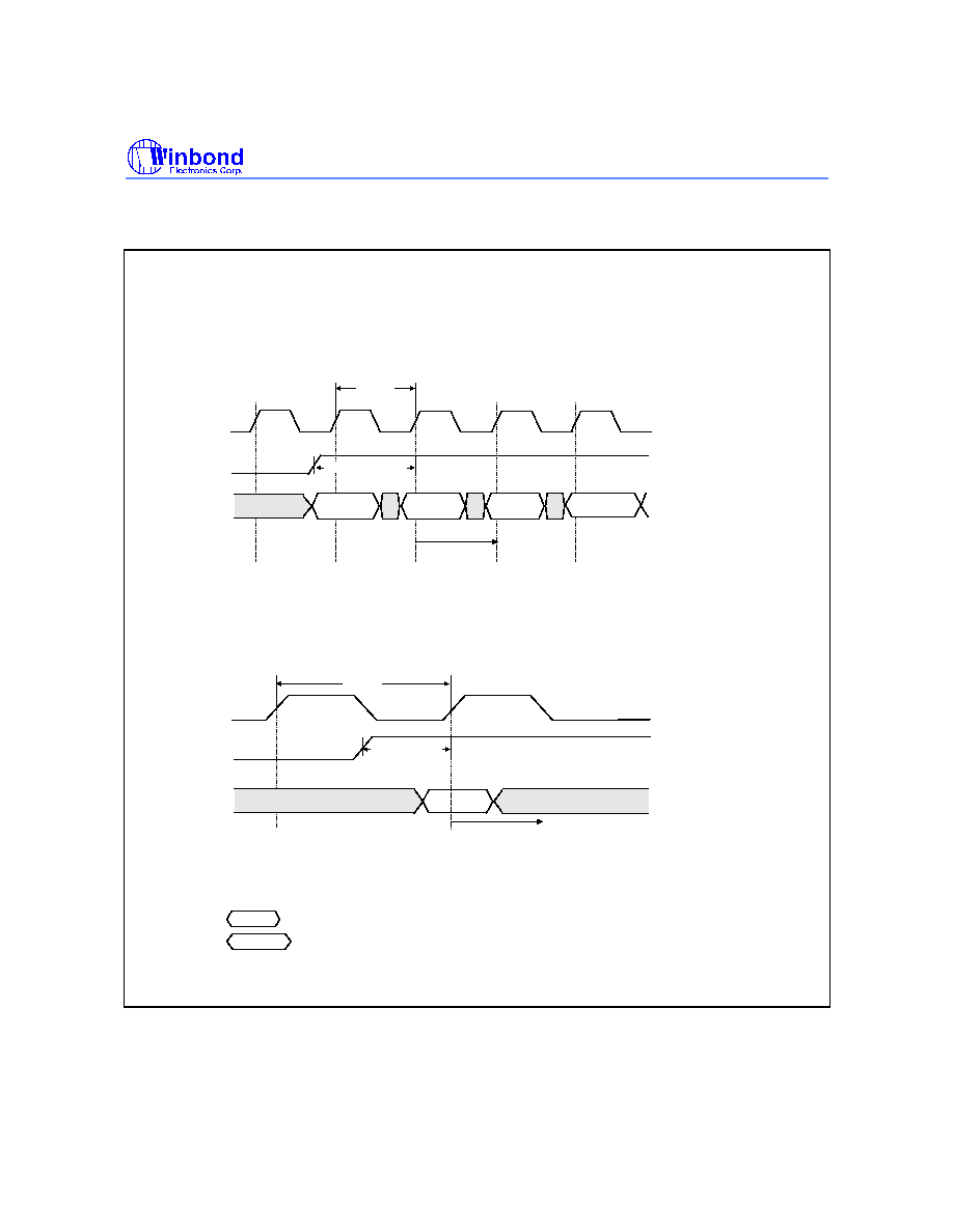
Self Refresh/Power Down Mode Exit Timing
Asynchronous Control
Input Buffer turn on time ( Power down mode exit time ) is specified by tCKS(min) + tCK(min)
Command
NOP
CLK
CKE
Command
A ) tCK < tCKS(min)+t CK(min)
Input Buffer Enable
Command
CLK
CKE
Command
B) tCK
>= tCKS(min) + t CK
(min)
Input Buffer Enable
Note )
Command
NOP
All Input Buffer(Include CLK Buffer) are turned off in the Power Down mode
and Self Refresh mode
Represents the No-Operation command
Represents one command
t
CK
t
CK
t
CKS
(min)+t
CK
(min)
t
CKS
(min)+t
CK
(min)
Preliminary W987Y6CB
Publication Release Date: May 21, 2002
- 45 - Revision A1
15. PACKAGE DIMENSION
FBGA 54 Balls (8 x 9 x 1.2 mm^3, ÿ = 0.40 mm)
Preliminary W987Y6CB
- 46 -
16. REVISION HISTORY
VERSION
DATE
PAGE
DESCRIPTION
A1
May 21, 2002
-
Initial Issued
Headquarters
No. 4, Creation Rd. III,
Science-Based Industrial Park,
Hsinchu, Taiwan
TEL: 886-3-5770066
FAX: 886-3-5665577
http://www.winbond.com.tw/
Taipei Office
TEL: 886-2-8177-7168
FAX: 886-2-8751-3579
Winbond Electronics Corporation America
2727 North First Street, San Jose,
CA 95134, U.S.A.
TEL: 1-408-9436666
FAX: 1-408-5441798
Winbond Electronics (H.K.) Ltd.
No. 378 Kwun Tong Rd.,
Kowloon, Hong Kong
FAX: 852-27552064
Unit 9-15, 22F, Millennium City,
TEL: 852-27513100
Please note that all data and specifications are subject to change without notice.
All the trade marks of products and companies mentioned in this data sheet belong to their respective owners.
Winbond Electronics (Shanghai) Ltd.
200336 China
FAX: 86-21-62365998
27F, 2299 Yan An W. Rd. Shanghai,
TEL: 86-21-62365999
Winbond Electronics Corporation Japan
Shinyokohama Kohoku-ku,
Yokohama, 222-0033
FAX: 81-45-4781800
7F Daini-ueno BLDG, 3-7-18
TEL: 81-45-4781881
9F, No.480, Rueiguang Rd.,
Neihu Chiu, Taipei, 114,
Taiwan, R.O.C.