PRELIMINARY DATASHEET
Publication Release Date: July 2003
- 1 -
Revision 1.0
WMS7170 / 7171
NON-VOLATILE DIGITAL POTENTIOMETERS
WITH UP/DOWN (3-WIRE) INTERFACE,
10KOHM, 50KOHM, 100KOHM RESISTANCE
100 TAPS
WITHOUT / WITH OUTPUT BUFFER

WMS7170 / 7171
- 2 -
1. GENERAL DESCRIPTION
The WMS7170/7171 is a single channel 100-tap non-volatile linear digital potentiometer available in
10K
, 50K and 100K resistance. The device consists of Up/Down serial interface, tap register,
decoder, resistor array, wiper switches, NV memory and control logics.
The WMS7170 device can be configured as a two-terminal variable resistor or a three-terminal voltage
divider without an output buffer, but the WMS7171 device, which has a built-in output buffer, can only
be configured as a three-terminal voltage divider. Both devices can be used in a wide variety of
applications.
The output of the potentiometer is determined by its wiper position, which varies linearly between its
end terminals, R
A
/V
A
and R
B
/V
B
. The wiper position, R
w
/V
w,
is controlled by Up/Down serial interface
(
CS
,
INC
and U/ D ) through the Tap Register (TR). In addition, the wiper position can also be
stored into a non-volatile memory location (NVMEM0), which is then automatically recalled upon
power up.
2. FEATURES
� Drop-in replacement for many popular parts
� Single linear-taper channel
� 100 taps
� 10K, 50K and 100K end-to-end resistance
� V
SS
to V
DD
terminal voltages
� Automatic recall of wiper position when power-on
� Potentiometer control through Up/Down (3-wire) serial interface
� Endurance 100,000 cycles
� Data retention 100 years
� Package options:
-
8-pin PDIP, SOIC or MSOP
� Industrial temperature range: -40� to 85�C
� Single supply operation : 2.7V to 5.5V

WMS7170 / 7171
- 4 -
4. TABLE OF CONTENTS
1. GENERAL DESCRIPTION.................................................................................................................. 2
2. FEATURES ......................................................................................................................................... 2
3. BLOCK DIAGRAM............................................................................................................................... 3
4. TABLE OF CONTENTS ...................................................................................................................... 4
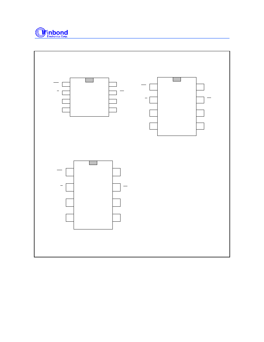
5. PIN CONFIGURATION ....................................................................................................................... 5
6. PIN DESCRIPTION ............................................................................................................................. 6
7. FUNCTIONAL DESCRIPTION............................................................................................................ 7
7.1. Rheostat And Divider Operations
........................................................................................... 7
7.1.1. Rheostat Configuration .......................................................................................................... 7
7.1.2. Divider Configuration.............................................................................................................. 7
7.2. Non-Volatile Memory (NVMEM0)
........................................................................................... 7
7.3. Serial Data Interface
................................................................................................................. 8
7.4. Operation Overview
.................................................................................................................. 8
8. TIMING DIAGRAMS............................................................................................................................ 9
9. ABSOLUTE MAXIMUM RATINGS & OPERATING CONDITIONS .................................................. 11
10. ELECTRICAL CHARACTERISTICS ............................................................................................... 12
10.1 Test Circuits
............................................................................................................................ 14
11. TYPICAL APPLICATION CIRCUITS............................................................................................... 15
11.1. Layout Considerations
.......................................................................................................... 17
12. PACKAGE DRAWINGS AND DIMENSIONS.................................................................................. 18
13. ORDERING INFORMATION........................................................................................................... 21
14. VERSION HISTORY ....................................................................................................................... 22