Publication Release Date 6/25/2002
WTS701
WINBOND SINGLE-CHIP TEXT-TO-SPEECH PROCESSOR
The information contained in this datasheet may be subject to change without
notice. It is the responsibility of the customer to check the Winbond USA website
(
www.winbond-usa.com
) periodically for the latest version of this document, and
any Errata Sheets that may be generated between datasheet revisions.
- 1 -
Revision 3.08

WTS701
- 2 -
1. GENERAL DESCRIPTION
The WTS701 is a high quality, fully integrated, single-chip Text-to-Speech solution that is ideal for use
in applications such as automotive appliances, GPS/navigation systems, cellular phones and other
portable products or accessories. The WTS701 product accepts ASCII (and Unicode for Mandarin)
input via a SPI port and converts it to spoken audio via an analog output or digital CODEC output.
The WTS701 integrates a text processor, smoothing filter and multi-level memory storage array on a
single-chip. Text-to-speech conversion is achieved by processing the incoming text into a phonetic
representation that is then mapped to a corpus of naturally spoken word parts. The synthesis
algorithm attempts to use the largest possible word unit in the appropriate context to maximize natural
sounding speech quality. The speech units are stored uncompressed in a multi-level, non-volatile
analog storage array to provide the highest sound quality to density trade-off. This unique, single-chip
solution is made possible through Winbond's patented multilevel storage technology. Voice and audio
signals are stored directly into solid-state memory in their natural, uncompressed form, providing
superior quality voice reproduction.
The chip can be programmed through the SPI port, allowing downloading of different languages and
speaker databases

WTS701
Publication Release Date: 6/25/2002
- 3 -
Revision 3.08
2. FEATURES
�
Fully Integrated Solution
Single-chip compact text-to-speech translation
No algorithm development required
Selectable digital and analog audio output
Simple SPI interface
Reprogrammable solution enables loading different voice or language
�
Text-To-Speech Algorithm Characteristics
High quality speech synthesis using speech element concatenation
Winbond's standard 100-year speech retention
Audio stored as uncompressed analog waveform � industry's highest quality and most natural
sounding
�
Easy to Use and Control
Real time conversion for streaming text
General text preprocessing and normalization
User customization for special characters such as SMS icons and chat emoticons
User customization for application specific abbreviations
�
Language Support
Support U.S. English and Mandarin (Beijing dialect)
Other languages in development or in planning
�
Device Management
Accepts ASCII or Unicode streaming text
256-byte text buffer
Playback of Phonetic Alphabet
Variable speed playback
Control of pitch change
Supports Power Down mode.
Supports Pause and Resume, Stop and Finish text conversion commands
�
Peripheral Control
16-bit linear PCM slave interface output support
SPI serial port for control commands and status report to system's host controller
Hardware handshake control signals
Analog audio output with 8
speaker driver and digital volume control
Analog audio input (AUXIN) for driving external audio to the speaker
�
Low Power Consumption
+2.7 to +3.3V (V
CC
) Supply Voltage
Operating Current:
I
CC Convert
= 35 mA (typical)
Standby Current:
I
SB
< 1
�A (typical)
�
Device Characteristics
Available in 56-lead TSOP package
Industrial temperature range (-40C to +85C)
3V/5V logic tolerance
WTS701
- 4 -
3. BLOCK DIAGRAM
3.1 WTS701 B
LOCK
D
IAGRAM
AUX OUT
V
SSA
V
CCA
V
SSA
V
SSD
V
SSD
V
CCD
V
CCD
Power Conditioning
RAM
FLASH
CODESTORE
MEMORY
(ROM)
SPI INTERFACE
REFERENCE
GENERATION
MLS
PHOENEME
MEMORY
HIGH VOLTAGE
GENERATION
PROCESSOR
13 BIT CODEC
LINEAR/ 2'S COMPLEMENT
SS\
MOSI
MISO
SCLK
MLS CONTROL
LOGIC
VCLK
VDX
VFS
SP+
SP-
Spkr.
AMP
AUX
OUT
AMP
CLOCK
GENERATION
XTAL1
XTAL2
ANALOG SIGNAL
CONDITIONING
AUXIN
AUX
AMP
R/B\
INT\
RESET
CS\
ATT CAP
Figure 1. WTS701 Block Diagram.
WTS701
3.2 WTS701 T
YPICAL
A
PPLICATIONS
HOST Controller
WTS701
SS\
MOSI
MISO
SCLK
VDX
VCLK
VFS
SP+
SP-
AUXIN
R/B\
INT\
CS\
AUXOUT
DIN
DOUT
CL
FS
CODEC
Processor
Baseband
Figure 2. WTS701 Configuration for Digital (CODEC) Environment.
HOST Controller
WTS701
SS\
MOSI
MISO
SCLK
VDX
VCLK
VFS
SP+
SP-
AUXIN
R/B\
INT\
CS\
AUXOUT
Line in
Line out
Figure 3. WTS701 Configuration for Analog Environment
Publication Release Date: 6/25/2002
- 5 -
Revision 3.08

WTS701
- 6 -
4. TABLE OF CONTENTS
1. GENERAL DESCRIPTION.................................................................................................................. 2
2. FEATURES ......................................................................................................................................... 3
3. BLOCK DIAGRAM .............................................................................................................................. 4
3.1. WTS701 Block Diagram ............................................................................................................. 4
3.2. WTS701 Typical Applications .................................................................................................... 5
4. TABLE OF CONTENTS ...................................................................................................................... 6
5. PIN CONFIGURATION ....................................................................................................................... 8
6. PIN DESCRIPTION............................................................................................................................. 9
7. FUNCTIONAL DESCRIPTION.......................................................................................................... 11
7.1. Text-to-Speech Mechanism ..................................................................................................... 12
7.1.1. Text Normalization ......................................................................................................... 12
7.1.2. Words-to-Phoneme conversation................................................................................... 12
7.1.3. Speech-element Mapping .............................................................................................. 12
7.2. Physical Interface..................................................................................................................... 13
7.2.1. Clocking.......................................................................................................................... 13
7.2.2. Power Down Mode ......................................................................................................... 14
7.2.3. Power and Grounding .................................................................................................... 14
7.2.4. SPI Interface................................................................................................................... 15
7.2.5. Flow Control Interface .................................................................................................... 16
7.2.6. The Codec Interface....................................................................................................... 16
7.2.7. The Analog Interface ...................................................................................................... 17
7.2.8. Resetting ........................................................................................................................ 18
7.3. Communication Protocol.......................................................................................................... 19
7.3.1. Command Classes ......................................................................................................... 20
7.3.2. Status Register............................................................................................................... 21
7.3.3. Interrupt Handler ............................................................................................................ 22
7.3.4. BCNT � Byte Count Register ......................................................................................... 23
7.3.5. Command Acceptance................................................................................................... 23
7.3.6. Data Acceptance ............................................................................................................ 23
7.4. Commands Overview .............................................................................................................. 23
7.4.1. Commands Description.................................................................................................. 26
7.4.2
Illegal Commands............................................................................................................ 37
7.4.3. Configuration Registers.................................................................................................. 38
7.4.4. System Operation........................................................................................................... 41
7.4.5. Initialization and Configuration ....................................................................................... 43

WTS701
Publication Release Date: 6/25/2002
- 7 -
Revision 3.08
7.4.6. Converting Text .............................................................................................................. 43
7.5. SPI Interface ............................................................................................................................ 45
7.5.1. SPI Transactions ............................................................................................................ 45
7.6. CODEC Interface ..................................................................................................................... 48
7.7. Phonetic Alphabet Playback .................................................................................................... 51
7.8. Customizing Abbreviations ...................................................................................................... 53
7.8.1. Abbreviation Data Format .............................................................................................. 54
7.8.2. Abbreviation Table Format............................................................................................. 54
7.8.3. Command Execution ...................................................................................................... 55
7.9. Device Programming ............................................................................................................... 55
7.10. Text-to-Speech Processor Commands � Quick Reference Table ........................................ 56
7.10.1. Text Input Format ......................................................................................................... 61
8. TIMING WAVEFORMS ..................................................................................................................... 63
8.1. SPI Timing Diagram ................................................................................................................. 63
8.2. CODEC Timing Diagrams ........................................................................................................ 65
9. ABSOLUTE MAXIMUM RATINGS.................................................................................................... 67
10. ELECTRICAL CHARACTERISTICS ............................................................................................... 68
11. TYPICAL APPLICATION CIRCUIT................................................................................................. 71
12. PACKAGE DIMENSIONS ............................................................................................................... 72
13. ORDERING INFORMATION........................................................................................................... 73
14. VERSION HISTORY....................................................................................................................... 73

WTS701
- 8 -
5. PIN CONFIGURATION
The following sections detail the pins of the WTS701 processor.
Table 1
shows all the pins and the signals that use them in different configurations. It also shows the
type and direction of each signal.
Figure 4
shows the physical pin out of the 56-pin TSOP package.
1
2
3
4
5
6
7
8
9
10
11
12
13
VSS A
W TS701
1
2
3
4
5
6
7
8
9
10
11
12
13
14
15
16
17
18
19
20
21
22
23
24
25
26
27
28
55
54
53
52
51
50
49
48
47
46
45
44
43
42
41
40
39
38
37
36
35
34
33
32
31
30
29
VCLK
VFS
VDX
M IS O
XT AL2
XT AL1
VSS D
VSS D
VCC D
VCC D
INT \
MOSI
S S\
S CLK
NC
NC
NC
NC
NC
NC
NC
NC
NC
NC
56
C S\
R/B\
R ESET
AUXOUT
AUXIN
VC C A
SP +
VS S A
SP -
AT T C AP
NC
NC
NC
NC
NC
NC
NC
NC
NC
NC
NC
NC
NC
NC
NC
NC
NC
NC
NC
NC
VS S A
Figure 4. 56-pin TSOP Package Connection Diagram.

WTS701
Publication Release Date: 6/25/2002
- 9 -
Revision 3.08
6. PIN DESCRIPTION
Table 1. WTS701 Pin Signal Assignment.
PIN NO.
SYMBOL
I/O
FUNCTION
13
INT\
O
Interrupt Output; an open drain output that indicates that
the device wishes an interrupt service. The device can
request an interrupt when it finishes an operation or needs
more data to process. Under what conditions the device
generates an interrupt can be configured through the user
configuration registers. This pin remains LOW until a Read
Interrupt command is executed.
26
R/B\
O
Ready/busy signal; This pin defaults HIGH indicating the
device is ready for data transfer. The pin is driven LOW to
handshake a pause in SPI data transfer.
7
XTAL2
O
CRYSTAL 2: This is the crystal oscillator output. It is the
inversion of XTAL1.
8
XTAL1
I
CRYSTAL 1: This is the crystal oscillator input. This pin
may be driven by an external clock. The clock to the
WTS701 processor is configured by a clock configuration
register, which is set by the host processor during the
initialization phase.
15
SS\
I
SPI Slave Select input. This is an active LOW input used
to select the device to respond to an SPI transaction.
16
SCLK
I
SPI Serial clock input.
6
MISO
O
SPI Master In, Slave Out pin. Serial data line used to
communicate with SPI master. Pin is tri-state when SS\=1.
14
MOSI
I
SPI Master Out, Slave In. Serial data input from Master
25
CS\
I
Chip Select (active LOW) Pin must be LOW to access
WTS701 device.
27
RESET
I
Global reset signal.
3
VCLK
I
CODEC master clock
4
VFS
I
CODEC frame synchronization signal
5
VDX
O
CODEC data output. This pin puts data out in the linear
PCM unsigned or 2's complement format. It is tri-stated
until the user requests a CONVERT operation.
52
AUXIN
I
Analog input pin. This pin should be capacitively coupled.
54
AUXOUT
O
Analog Output for single ended output from the device.
46 SP+ O
Differential
Positive Speaker Driver Output.
42 SP- O
Differential
Negative
Speaker Driver Output.
WTS701
- 10 -
40 ATTCAP I/O AutoMute
Capacitor
Pin. Should have a 4.7uF capacitor to
VSSA.
11,12
VCCD
P
Positive Digital Supply pin. These pins carry noise
generated by internal clocks in the chip. They must be
carefully bypassed to Digital Ground to ensure correct
device operation.
9,10
VSSD
G
Digital Ground pin.
2,36,44
VSSA
G
Analog Ground pins.
48
VCCA
P
Positive Analog Supply pin. This pin supplies the LOW
level audio sections of the device. It should be carefully
bypassed to Analog Ground to ensure correct device
operation.
1,17-
24,28-
35,37-
39,41,43,
45,47,49-
51,53,55-
56
NC
Not Connected � must be floating.
Note: TYPE I:Input, O:Output, I/O bi-directional, P:Power, G:Ground

WTS701
Publication Release Date: 6/25/2002
- 11 -
Revision 3.08
7. FUNCTIONAL DESCRIPTION
As a real System-On-Chip solution, the WTS701 performs the overall control functions for host
controller and text-to-speech processing.
The WTS701 system architecture consists of the following functions:
� Serial interface to monitor the SPI port and interpret commands and data
� Text normalization module to pre-process incoming text into pronounceable words
� Words to phoneme translator, which converts incoming text to phoneme codes
� Phoneme mapping module that maps incoming phonemes to words, sub-words, syllables or
phonemes present in the MLS memory
� Volume and speed adjustments
� Digital and analog output blocks for off-chip usage
The WTS701 system performs text-to-speech synthesis based on concatenative samples. The units
for concatenation can vary from whole words down to phoneme units. The convention is that the
larger the sub-word unit used for synthesis the higher the quality of the speech output. A corpus of
pre-recorded words is stored in Winbond's patented multilevel storage (MLS) memory and a mapping
of the various sub-word parts is held in a lookup table. The speech creation is achieved by
concatenation of these speech elements to produce words. The system process flow is shown in
Figure 5.
Text Normalization
Words to Phoneme
Phoneme Mapper
MLS
Memory
Digital
output
Analog
output
WTS701
Speech
Serial Text,
symbols &
Control
Figure 5. WTS701 System Process Flow.

WTS701
- 12 -
7.1
T
EXT
-T
O
-S
PEECH
M
ECHANISM
The text to speech component of the system consists of three principal blocks:
� Text normalization
� Word to phoneme conversion
� Phoneme mapping
7.1.1 Text Normalization
Text normalization involves the translation of incoming text into pronounceable words. It includes such
functions as expanding abbreviations and translating numeric strings to spoken words. It involves a
certain amount of context processing to determine correct spoken form.
In addition, the WTS701 looks into abbreviation list stored in the device's internal memory and
converts acronyms, abbreviations or special characters (such as Instant Messaging icons or
emoticons) into the appropriate text representation.
The default abbreviation list supported by the WTS701 is a general one that can be modified by the
user to match the domain that the text is being loaded from. This enables a flexibility of adding
abbreviation specifically for the text either by the developer or even the end user to best customize the
product for its preferences. Instant Messaging or Short Messages Service (SMS) unique characters
are supported through this functionality as well, defining the icon ASCII/Unicode text and its
replacement. The default abbreviation list supported is described in the specific language release
letter.
7.1.2 Words-to-Phoneme conversion
Once the data stream has been translated to pronounceable words, the system next determines how
to pronounce them. This function is obviously highly language dependent. For a language such as
English it is impossible to break this task down to a set of definitive rules. The task is achieved by a
combination of rule based processing together with exception processing.
7.1.3 Phoneme Mapping
This algorithm maps phoneme strings into the MLS phonetic inventory. This task falls into two
portions. First, the word must be split into sub-word portions. This splitting must be done at
appropriate phonetic boundaries to achieve high quality concatenation. Once a sub-word unit is
determined, the inventory is searched to determine if a match is present. A matching weight is
assigned to each match depending on how closely the phonetic context matches. Each sub-word has
a left and right side context to match as well as the phoneme string itself. If no suitable match is found

WTS701
Publication Release Date: 6/25/2002
- 13 -
Revision 3.08
in the inventory, then the sub-word is further split in a tree like manner until a match is found. The
splitting tree is processed from left to right and each time a successful match occurs the address and
duration of the match in the corpus is placed in a queue of phonetic parts to be played out the audio
interface.
7.2
P
HYSICAL
I
NTERFACE
The following sections describe the physical pin properties and the timing associated with the physical
interface to the device. Note that all input pins are 3V and 5V tolerant, except for the CS\ signal which
is only 3V tolerant.
7.2.1 Clocking
The WTS701 processor can receive its clock from either external clock source or crystal oscillator
The XTAL1 and XTAL2 pins provide the crystal interface to the device. The clock to the WTS701
processor is configured by a clock configuration register, which must be set by the host processor
during the initialization phase.
Figure 6
below shows how to connect the WTS701 to a crystal
oscillator. An external clock can be connected to the WTS701 providing the clock source for the
system, as shown in
Figure 6.
WTS701
XTAL1
XTAL2
WTS701
XTAL1
XTAL2
CLK IN
X1
C1
C2
C1 = C2 = 5pF
X1 = 24.576MHz
Figure 6. Clock Generation.

WTS701
- 14 -
7.2.2 Power Down Mode
Upon application of power, the WTS701 will enter the RESET state and then be in a POWER DOWN
state. In the POWER DOWN mode, only Class0 SPI commands are valid. (See subsection
7.3.1
). The
Power Down status of the device can be determined with a RDST (Read Status) command, specified
by the RDY bit in STATUS BYTE 0.
Issuing the PWDN (Power Down) command to the WTS701 processor will return the processor to the
POWER DOWN mode. In POWER DOWN mode the external crystal oscillator is shut off and the
processor is deactivated. POWER DOWN mode is exited by issuing a PWUP (Power Up) command
to the WTS701. The PWUP command should be preceded by a SCLC (Set Clock) command to
ensure correct clock configuration.
7.2.3 Power and Grounding
The WTS701 can operate over 2.7V to 3.3V supply voltage range. The power supply and ground pins
(V
CCA
,
V
CCD
,
V
SSA
,
V
SSD
) should be carefully bypassed as close to the chip as possible to ensure high
quality audio. In addition, ATTCAP pin should have a 4.7 �F capacitor connected to ground. This pin
must not be left floating. The pins that are marked as NC (Not Connected), should be left floating.
V
CCA
, V
CCD
(Voltage Inputs)
To minimize noise, the analog and digital circuits in the WTS701 device use separate power busses.
These +3.0 V busses lead to separate pins. For optimal noise immunity, tie the V
CCD
pins together as
close as possible and decouple both supplies as near to the package as possible.
V
SSA
, V
SSD
(Ground Inputs)
The WTS701 series utilizes separate analog and digital ground busses. The analog ground (V
SSA
)
pins should be tied together as close to the package as possible and connected through a low-
impedance path to power supply ground. The digital ground (V
SSD
) pin should be connected through a
separate low-impedance path to power supply ground. These ground paths should be large enough to
ensure that the impedance between the V
SSA
pins and the V
SSD
pin is less than 3
. The backside of
the die is connected to V
SSD
through the substrate resistance.
NC (Not Connect)
These pins should not be connected to the board at any time. Connection of these pins to any signal,
ground or V
CC
may result in incorrect device behavior or cause damage to the device.

WTS701
Publication Release Date: 6/25/2002
- 15 -
Revision 3.08
7.2.4 SPI Interface
Communications with the WTS701 is conducted over the SPI serial communications port. The device
responds to a command when the Chip Select signal (CS\) is LOW and addressed by an active LOW
signal on the SS\(Slave Select) pin. Under this condition, it accepts data on the MOSI input, which is
clocked in on rising edges of the serial clock (SCLK) signal. Concurrently, valid data from the WTS701
device to the bus master is available on MISO for the HIGH period of SCLK. The protocol
implemented on the WTS701 defines that the first two bytes of data sent in an SPI transaction is a
command word. A transaction is defined as the SPI transfers conducted while SS\ is LOW, the
transaction ends when SS\ returns HIGH. List of available commands can be found in subsection
7.10
(Text-To-Speech Processor Commands Quick Reference Table).
All Input pins are 3V and 5V tolerant, except for the CS\ signal which is only 3V tolerant.
The following is a description of the WTS701 SPI interface signals:
SCLK (Serial Clock)
The Serial Clock line is a digital input. It is driven by the SPI master and controls the timing of the data
exchanged over the SPI data lines, MOSI and MISO. The maximum frequency of the clock rate for
this pin is 5MHz.
SS\ (Slave Select)
The Slave Select line is an active LOW digital input. It is driven by the SPI master and acts as a chip
select line. The device only responds to SPI transactions when this line is selected (LOW) and then
raised HIGH after SPI communication ends.
CS\ (Chip Select)
The Chip Select line is an active LOW digital input. It can be driven by the host controller to enable
SPI transactions to the device. Normally this pin is tied LOW unless more than one device is to share
the same SS\ signal.
MOSI (Master Out, Slave In)
The MOSI line is a digital input. MOSI is driven by the SPI master. It provides data transfer from the
master to the slave.
MISO (Master In, Slave Out)
The MISO line is a digital output. When SS\ is HIGH, this pin is tri-state. When SS\ is LOW, MISO is
driven by the device. It provides serial data transfer from the slave to the master.

WTS701
- 16 -
7.2.5 Flow Control Interface
In addition to the SPI interface, the WTS701 has two control lines to facilitate data transfer and host
communications. The INT\ (interrupt) pin is used by the WTS701 to request an interrupt service
from the host controller. The interrupt types that the device generates are controlled by the
communications control register command (SCOM). The R/B\ (ready/busy) pin is used to control the
flow of data across the SPI bus. When this signal is HIGH, the device can accept more data. When
it is LOW, SPI transactions must be paused or terminated.
INT\ (Interrupt)
INT\ is an open drain output pin. The WTS701 interrupt pin goes LOW and stays LOW when an
interrupt event has occurred, as defined by the SCOM command. The interrupt is cleared when a
RINT (read interrupt) command is executed. The status register defines what type of interrupt has
occurred.
R/B\ (Ready/Busy Signal)
The R/B\ line is an output pin used to control data transfer rate across the SPI port. The line is used
as a handshake signal to the SPI Master to indicate when the device is ready for more data. When
HIGH, the master is free to send more data. When LOW, the device is busy and cannot accept more
data.
7.2.6 The CODEC Interface
The WTS701 provides an on chip interface for digital environment systems, supporting slave CODEC
interface mode. The WTS701 CODEC interface is controlled by an external source hence the
WTS701 only transmits data. Thus, it is effectively an analog-to-digital converter. Each analog
sample is converted to 10 bit digital word. This digital word is transmitted with the MSB first. Since
the host expects either 13 or 16 bit data in the short frame format, either three or six zeros are
appended as the LSB. It interfaces to the baseband CODEC via the VCLK, VFS and VDX lines.
Refer to
Figure 2
, for more information about the connection between the WTS701 and a CODEC.
All Input pins are 3V and 5V tolerant.
The following is a description of the WTS701 CODEC interface signals:
VCLK (CODEC Clock Line)
The CODEC clock line supplies the sampling clock to the internal CODEC. This is a digital input and
expects a 512kHz--2.048MHz clock.
WTS701
Publication Release Date: 6/25/2002
- 17 -
Revision 3.08
VFS (CODEC Synchronization Line)
The CODEC synchronization line supplies a frame synchronization signal to the internal CODEC. This
is a digital input. After receipt of a synchronization pulse, the CODEC will output data on the VDX
line. The VFS line expects an 8kHz sample rate and supports both short frame and long frame
synchronization signal.
VDX (CODEC Data Transmit Line)
The CODEC data transmit line is a digital output that places digital audio data onto the CODEC bus.
The line is in a tri-state condition until the device is due to transmit data. The data output from the
VDX line is selected by the SCOD Command. When WTS701 places data on the VDX line, it is
required that the VFS line should be in tri-state condition when another device is connected to the
CODEC as well.
7.2.7 The Analog Interface
The WTS701 provides an on chip analog interface for audio output via an 8
speaker driver or an
output buffer capable of driving a 5k
load. Additionally, an analog input (AUXIN) allows an audio
signal to be fed through the WTS701 chip to either output device. The command SAUD configures
the analog path. A digitally controlled attenuator provides volume control via the SVOL command.
The following is a description of the analog pins:
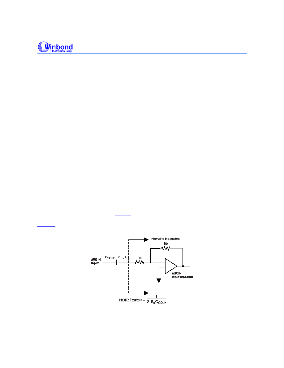
AUXIN (Analog Input)
The AUXIN is an additional audio input to the WTS701. This input has a nominal 694 mV p-p level at
its minimum gain setting (0 dB) (See
Table 2
). Additional gain is available in 3 dB steps (controlled
by the SAUD Command) up to 9 dB. The use and equivalent circuit of the input amplifier is shown in
Figure 7.
Figure 7. AUXIN Input Amplifier.

WTS701
- 18 -
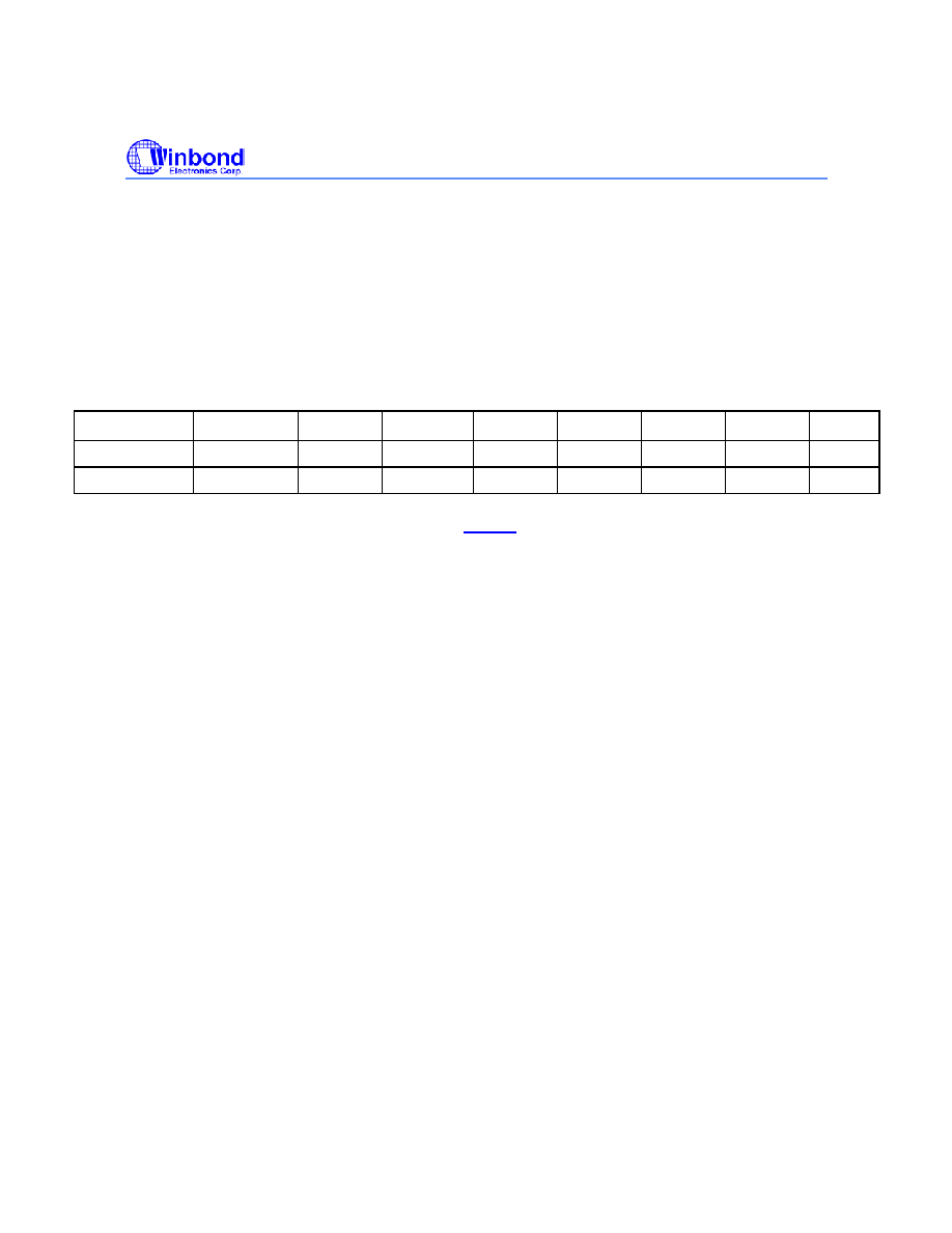
Table 2. AUXIN Gain Settings.
AUD Register
0TLP Input
V
P-P
1
AIG1 AIG0
Gain
2
Gain
2
(dB)
Resistor
Ratio (R
b
/R
a
)
Speaker
Out V
P-P
3
0.694
0
0
1.00
0
40.1 / 40.1
0.694
0.491
0
1
1.41
3
47.0 / 33.2
0.694
0.347
1
0
2.00
6
53.5 / 26.7
0.694
0.245
1
1
2.82
9
59.2 / 21
0.694
1
OTLP Input is the reference Transmission Level Point that is used for testing. This level is typically 3 dB below clipping.
2
From AUXIN to AUXOUT.
3
Measured differentially at SP+/SP.
AUXOUT (Analog Output)
The AUXOUT is an audio output pin used to provide an analog output of the synthesized speech from
the WTS701. It drives a minimum load of 5 k
up to a maximum of 1 V p-p. The AC signal is
superimposed on approximately 1.2 VDC bias and must be capacitively coupled to the load. This
output stage may be powered down by clearing the AOPU bit via the SAUD command.
SP +, SP- (Speaker +/-)
This is the speaker differential output circuit. It is designed to drive an 8
speaker connected across
the speaker pins up to a maximum of 23.5 mW power. This stage has selectable gains of 1.32 and
1.6, which can be chosen through the SPGO bit via the SAUD command. These pins are biased to
approximately 1.2 VDC and, if used single-ended, must be capacitively coupled to their load. Do
NOT
ground the unused pin. This output stage may be powered down by clearing the SPPU bit via
the SAUD command.
ATTCAP (AutoMute Attenuator Capacitor)
This pin provides a capacitor connection for setting the AutoMute. It should have a 4.7 �F capacitor
connected to ground and it cannot be left floating. The AutoMute circuit reduces the amount of noise
present in the output during quiet pauses.
7.2.8
Resetting
The chip has an internal power-on reset circuit that ensures correct initialization upon application of
power. The reset pin signal must be held HIGH for 0.5
�s to achieve a reset (see
Figure 8
) and to put
the WTS701 in the RESET state. Once the WTS701 completes the reset, it will enter the POWER
DOWN mode. Before issuing active commands, a clock configuration and device power up command
must be issue in the POWER DOWN mode.
Issuing a Reset command (RST) resets the WTS701 processor to the initial POWER DOWN state.
Applying the reset pin, while the chip is active, allows the host processor to reset the WTS701 to its
default values and the IDLE state.

WTS701
Publication Release Date: 6/25/2002
- 19 -
Revision 3.08
T
res et
T
res et
> 0.5
�
s
RESET
Figure 8. Reset Condition Timing.
7.3
C
OMMUNICATION
P
ROTOCOL
The WTS701 is controlled by a series of SPI transactions to send commands to the device. The
general format of an SPI transaction is shown in
Figure 9.
A transaction is always started by sending
a command word. The command word consists of a command byte followed by a command data
byte. At the same time, the status register is shifted out on the MISO line. What follows depends on
what command is sent. The general case is that following the command word, up to n-bytes of data
can be sent to the device and n-bytes can be read from the device. An SPI transaction is finished
when SS\ is returned to the HIGH condition.
DATAn
DATA1
DATAn
DATA1
DATA0
DATA0
CMD DATA
STATUS BYTE 1
CMD BYTE
STATUS BYTE 0
MOSI
MISO
MSB
LSB
time
Figure 9. SPI Transaction Format.

WTS701
- 20 -
7.3.1 Command Classes
The SPI transactions to the WTS701 fall into four classes. The four classes represent variations in
how the command, and any associated data, is handled. The class of a command is defined by the
two most significant bits of the command byte. A summary of the command classes is given below
Class 0 Commands
These are commands that are executed irrespective of the state of the WTS701. That is, the
command will execute even if the device is busy or powered down. These commands are executed
internally by a hardware command interpreter. All commands not of class 0 require that the WTS701
be in a powered up state. Example of class 0 command is the Read Status (RDST) command.
Class 1 Commands
Class 1 commands require interpretation by the internal firmware of the WTS701. Class 1
commands consist only of a command byte and command data byte. Any further data sent in a
transaction is ignored. Class 1 commands are most often used for setting a configuration register in
the device or sending commands that have no data such as the conversion pause (PAUS) command.
Class 2 Commands
Class 2 commands have associated data. After the command word, any data bytes following are
loaded into an internal FIFO buffer for processing. If this FIFO becomes full, the R/B\ signal is
asserted (LOW) indicating that the host must pause data transfer. An alternative to monitoring the
R/B\ line, the R/B\ bit of the status register can be monitored instead (see subsection
7.3.2
) or via the
RDST command.
Class 3 Commands
Class 3 commands have data to return to the host. The R/B\ line will go to busy immediately
following the command word indicating that the WTS701 is fetching the requested data. Data is put
into the BCNT0 and BCNT1 (see subsection
7.3.4
) registers and is read out in the two subsequent
bytes after R/B\ is released. If more than two bytes are returned from the command, R/B\ will again
be asserted until data is ready to read. The primary Class 3 commands are to read the contents of
internal configuration registers such as RREG command.
WTS701
Publication Release Date: 6/25/2002
- 21 -
Revision 3.08
7.3.2 Status Register
The WTS701 has a sixteen-bit status register whose value is returned to the host controller during the
command word. For class 2 commands, the status register is repeatedly returned every two bytes.
This status register provides the host with information regarding the current status of the chip. The
host can decide on required actions with this information. The Status Register is echoed back by all
commands.
Table 3. Status Bytes.
Bit 7
Bit 6
Bit 5
Bit 4
Bit 3
Bit 2
Bit 1
Bit 0
Status Byte 0
ICNT IBUF ICNV COD
BFUL
BEMP
CNVT
RDY
Status Byte 1
R/B\ Reserved
Reserved
Reserved Reserved
IABB
Reserved
ICMD
The contents of the status bytes are described in
Table 4
.

WTS701
- 22 -
Table 4. Status Bit Description.
Byte
Bit Name
Bit #
RDY
0
Ready to accept commands. After the device has been powered up,
this bit is set after the Power Up latency delay.
CNVT
1
Converting. This bit is set anytime while the conversion process is
running. If this bit is clear when a convert command is sent, the count
in the Count register is set to 0.
BEMP
2
The input buffer is empty. This bit is set anytime the input buffer is
empty.
BFUL
3
The input buffer is full. This bit is cleared after 128 bytes become
available in the input buffer.
COD
4
CODEC is enabled. This is set when the CODEC has been enabled
by the SCOD command.
ICNV 5
Conversion
finished
interrupt has occurred. To stop CODEC
transmission or Power Down the analog outputs an IDLE command
should be sent. This bit is cleared by RINT command.
IBUF
6
The input text buffer been filled above the defined threshold and then
gone below the defined threshold. The buffer threshold level is set by
the SCOM command. If set by the SCOM command, the INT\ pin will
also go LOW. This bit is cleared by RINT command.
Status Byte 0
ICNT
7
Count interrupt has occurred. This interrupt is generated every time a
word has been spoken if activated by the SCOM command. This bit is
cleared by RINT command.
ICMD
0
Command was ignored. Anytime ICMD is set, the transaction must
revert to a single word command and the command must be resent.
Any data sent will be ignored.
IABB
2
Abbreviation interrupt has occurred, abbreviation add or abbreviation
delete has been completed. Now the ENTER_RRSM command can
be sent.
Status Byte 1
R/B\
7
Current state of the R/B\ pin. If this bit is 0, any data sent will be
ignored.
*5 bits are reserved.
7.3.3 Interrupt Handler
If an interrupt has occurred, no further interrupts will be registered until the first interrupt has been
cleared. Only one interrupt can be active at any time.
The RINT command will read and clear pending interrupts while the RDST command will read
interrupts without clearing them.
Make sure that all interrupts that are not being used are masked by clearing the corresponding bits in
the COM register.

WTS701
Publication Release Date: 6/25/2002
- 23 -
Revision 3.08
7.3.4 BCNT -- Byte Count Register
The byte count register (BCNT) is a tool for the host to keep track of where in a conversion the
WTS701 is. When a new conversion is started, the byte count register is reset to zero. As each
word (as defined by white-space separated characters) is spoken, the byte count register is updated
to point to the first character of the next word to be spoken. In this way, the host can position a new
conversion if the user wishes to repeat or skip text. The BCNT register is sent with BCNT1 (MSB)
first and BCNT0 (LSB) second.
7.3.5 Command Acceptance
The WTS701 processes commands and data as they are sent to the device. Under certain
conditions the device will not be ready to accept a new command or data. If the device has not
finished processing the previous command, the ICMD bit of the status register will be set. If this bit is
set, it implies that device is not in a position to accept the command being sent and that it will be
ignored. The host should monitor this bit when a command is sent and, if it is detected, the SPI
transaction should be terminated at the end of the command word. The host can then resend the
command until the command is accepted.
7.3.6 Data Acceptance
The WTS701 has an eight byte FIFO to buffer data from the SPI port to the internal processor.
During a conversion, data is read from this FIFO into an internal RAM data buffer. If SPI
transmission is too fast for the WTS701 to keep up with the R/B\ line will be asserted (LOW) to pause
data transfer. Alternatively, the STATUS register can be monitored for the state of the R/B\ signal.
7.4
C
OMMANDS
O
VERVIEW
Control of the WTS701 is implemented through a 16-bit command word. The command word is
always the first word to follow the falling edge on the SS\ signal. The command word consists of the
command byte followed by the command data byte. Many commands do not require a command
data byte, although one must be sent. For commands that have no data, the command data byte is a
`don't care'.
Commands fall into five categories. Commands that control an operational synthesis function of the
text-to-speech processing, commands that modify internal configuration registers, commands that
change system state, commands that read internal status registers, and customization commands.

WTS701
- 24 -
Status Commands
Table 5. Status Opcodes.
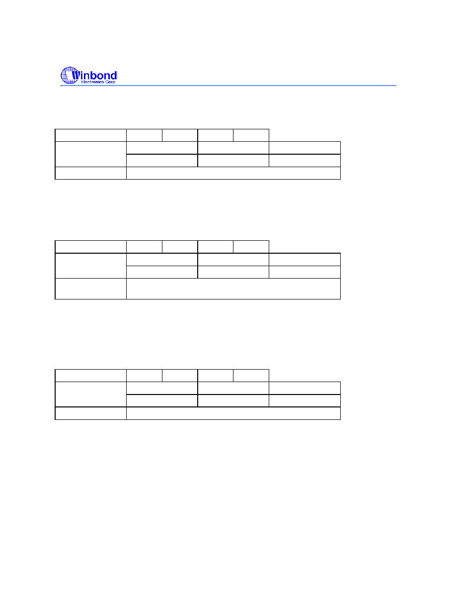
The WTS701 has three read-only
registers accessed by the opcodes,
which are shown to the right.
� The Read Status Register
returns the device's
operational status and the
numbers of bytes that have been converted.
Opcode Mnemonic
Function
0x04
RDST
Read Status Register
0x06
RINT
Read Interrupt Register
0x12 RVER Device
Version
� The Read Interrupt Register returns the same status data and clears any of the interrupt
status bits that are set.
� The version register returns the device and language version of the chip.
System Commands
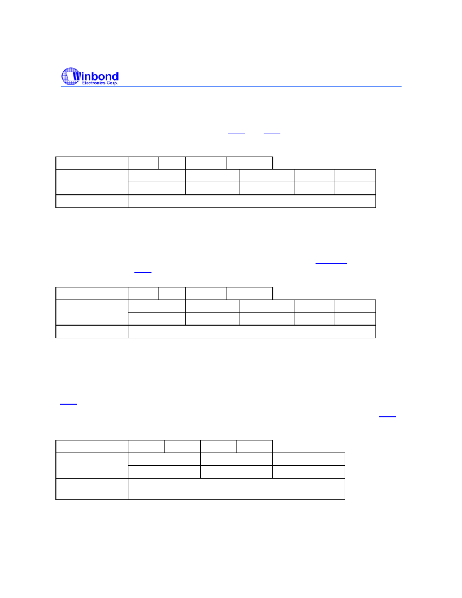
Table 6. System Opcodes.
The WTS701 responds to various
system commands that change the
state of the system, namely:
� The Power Up command
wakes up the device from
POWER DOWN mode.
� The Power Down
command requests that the device enter the POWER DOWN mode.
Opcode Mnemonic Function
0x02 PWUP Power
Up
0x40 PWDN Power
Down
0x10 RST
Reset
0x57 IDLE
Go
Idle
� The Reset command resets the device (see subsection
7.4.3
).
� The Idle command puts WTS701 processor in IDLE mode

WTS701
Publication Release Date: 6/25/2002
- 25 -
Revision 3.08
Synthesis Commands
Table 7. Synthesis Opcodes.
The synthesis commands affect the
text-to-speech synthesis. They are
detailed in the table to the right.
The basic commands are:
� Start a conversion
� Pause the conversion
� Resume the conversion
� Stop the conversion
� Finish conversion at the
end of the next word.
Opcode Mnemonic
Function
0x81 CONV Start
Converting
0x49 PAUS Pause
Conversion
0x4A RES Resume
Conversion
0x4B ST
Stop
Conversion
0x4D FINW Finish
Word
0x4C FIN Finish
Buffer
0x53 VLUP Volume
Up
0x54 VLDN Volume
Down
0x55
SPUP
Speed Up Conversion
0x56
SPDN
Slow Down Conversion
� Finish the conversion at the
end of the buffer
� Volume up/down
� Speed up/down the text-to-
speech conversion
Configuration Commands
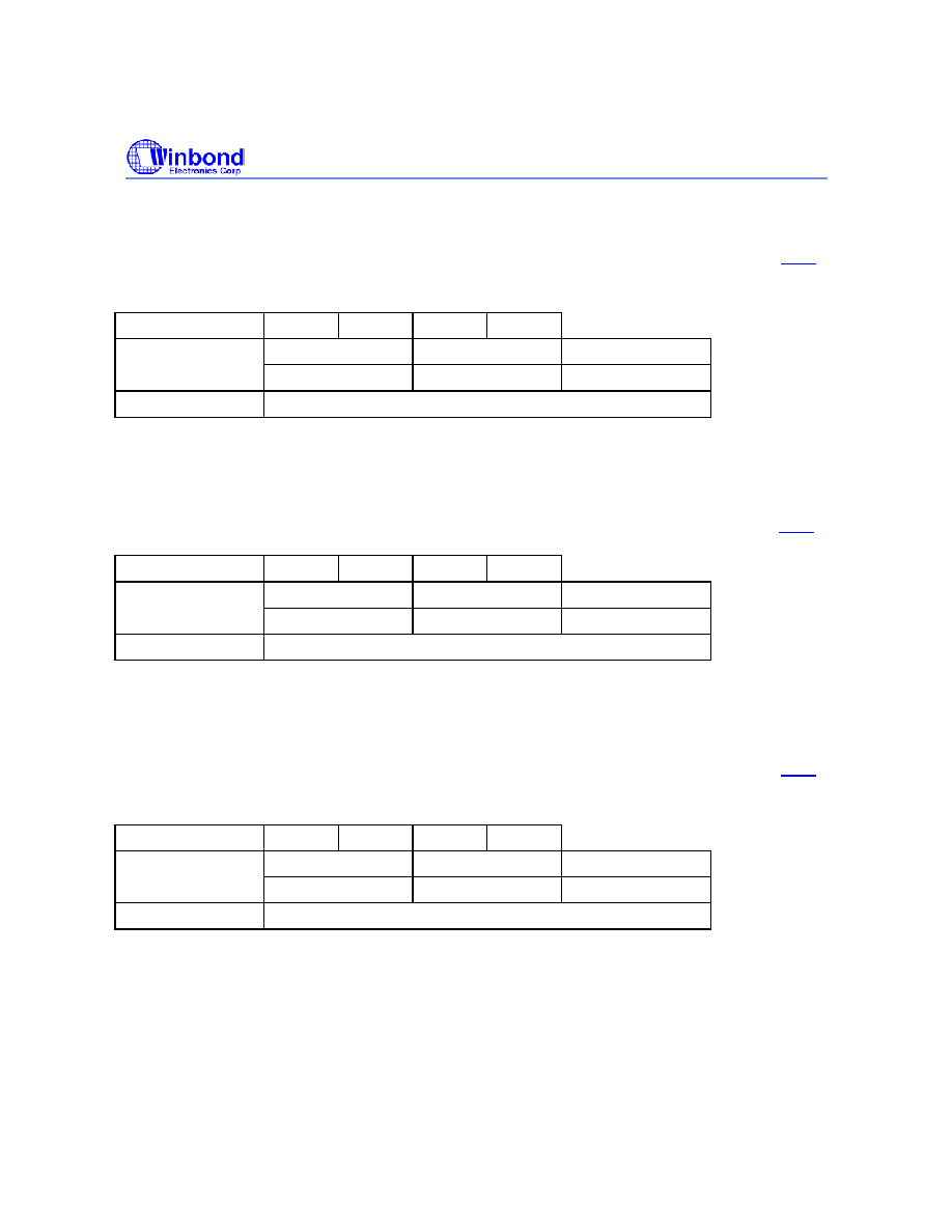
Table 8. Configuration Opcodes.
The WTS701 has several configur-
ation registers. The commands are:
Opcode Mnemonic
Function
0xC0
RREG
Read Configuration register
0x4E
SCOM
COM Configuration register
0x4F
SCOD
CODEC Configuration register
0x50
SAUD
AUDIO Configuration register
0x51
SVOL
VOL Configuration register
0x52
SSPD
SPEED Configuration register
0x14 SCLC
CLC
(Clock)
Configuration
register
0x77
SPTC
Set Speech Pitch
� The COM configuration
register governs the behavior
of how the chip uses the INT\
and R/B\ hardware lines to
communicate with the host
� The CODEC register con-
figures the mode of the digital
audio output
� The AUDIO register sets
parameters of the analog
audio path
� The VOLUME register sets the volume level of output
� The SPEED register sets the speed level of output speech
� The CLC register sets the master clock frequency of the device
� The SPTC command sets speech pitch

WTS701
- 26 -
Customization Commands
Table 9. Customization Opcodes.
The WTS701 has the ability for the
user to customize the way in which
it responds to certain text strings.
This is done by way of an
abbreviation table. The
customization opcodes allow the
user to interrogate and modify the
abbreviation table.
Opcode Mnemonic
Function
0xC8
ABBR_NUM
Get number of abbrev. entries
0xC9
ABBR_RD
Read abbreviation table
0xC7
ABBR_MEM
Get number of free bytes.
0xAF
ABBR_ADD
Add abbrev. entry
0x83
ABBR_DEL
Delete abbrev. entry
0x0C ENTER_RRSM
Swap
memory
7.4.1 Command Description
The following section list all the standard commands that can be executed on the WTS701.
PWDN Go to POWER DOWN Mode
This command puts the WTS701 processor in power-down mode. This is a single word command
therefore no data is required for this command. The Power Down command places the WTS701
device into its lowest power consumption mode. In POWER DOWN mode, the device will only
respond to a Power Up command (PWUP) and Read Status (RDST) command. As soon as Power
Down sequence has ended, the RDY flag in the status word is cleared.
PWDN
Class 1
Type I
Host controller
0x40
0x00
Byte Sequence:
WTS701
Status Byte 0
Status Byte 1
Description:
Put the WTS701 processor in power-down mode.
PWUP Power Up
This command wakes up the WTS701 processor to IDLE state. The result of this command is that
the WTS701 starts the power up sequence, which leads to bringing up internal supplies, resetting the
processor, all configuration registers are initialized to their default values and entering IDLE state. As
soon as power up sequence has ended, the RDY flag in the status word is asserted. The SCLC
command must be sent BEFORE PWUP.
WTS701
Publication Release Date: 6/25/2002
- 27 -
Revision 3.08
PWUP
Class 0
Type I
Host controller
0x02
0x00
Byte Sequence:
WTS701
Status Byte 0
Status Byte 1
Description:
Wake up the WTS701 processor to IDLE state.
CONV
Convert
The convert command starts the text to speech conversion process. The convert command is
followed by ASCII text data. The device has a buffer of 256 bytes. When this buffer is full, the chip
pulls the R/B\ line LOW and sets the BFUL bit in the status word indicating that the WTS701 buffer
manager is in the buffer full condition. The WTS701 remains in the buffer full condition until the input
buffer has been emptied of half the buffer space (128 bytes). When the buffer is full, the Host may
do one of two things:
1. The Host may end the command at that point, then poll the BFUL bit of the SPI status register until
it is clear, and then send new CONV commands with the additional ASCII text data.
2. The Host may also continue the command (keep SS\ LOW) and wait for the R/B\ pin to go HIGH.
As each word is processed by the WTS701, space will become free in the buffer and the R/B\ pin
will go HIGH until it is full again.
The device may also be configured such that it will generate an interrupt to the host when the buffer
threshold (set by RCOM command) has been crossed. (See
Tables 3
and
4
) This allows the host to
fill the buffer then wait for the Interrupt to send the additional data.
During conversion, the Convert Count Register is updated as each word has been spoken. This
register is cleared to zero at power up, and at the beginning of a new conversion process after one
has been terminated.
A convert command is terminated in several ways:
� The first is to send a finish command (FIN) indicating that the host has finished sending data.
In this case, the device finishes converting the text buffer, then stops and enters a wait state.
� The conversion process will also stop when the EOT (^D, ASCII 0x1A, UNICODE 0x00 0x1A)
character is part of the input text. When the device detects the EOT character, it will continue
the conversion process until the buffer is emptied and the final word spoken. Then it will stop
and enter the wait state.
� The finish word command (FINW) will cause the WTS701 device to finish the word currently
being spoken, then flush the buffers and enter the wait state.
� The stop command (ST) will cause the WTS701 to immediately stop converting, flush the
buffer and enter the wait state.
WTS701
- 28 -
Once the wait state has been entered the device will clear the convert (CONV) bit from the status
register and, if enabled, generate an ICVT interrupt. At this stage the CODEC and analog path are
still active. To release the CODEC bus or Power Down the analog path an IDLE command should be
sent to the device.
CONV
Class 2
Type
III
Host controller
0x81
0x00 DATA0
...
DATAn
Byte
Sequence:
WTS701
Stadus Byte 0
Status Byte 1 Status Byte 0 ... Status Byte n%2
Description:
Start or continue a conversion process. Data sent is text data for conversion.
PAUS
Pause
This command causes a pause of the conversion process. There is no data associated with this
command. The pause condition is terminated by the RES (Resume) command
PAUS
Class 1
Type I
Host controller
0x49
0x00
Byte Sequence:
WTS701
Status Byte 0
Status Byte 1
Description:
This command pauses the conversation process.
RES
Resume
This command causes the conversion to resume if it was paused. There is no data associated with
this command
RES
Class 1
Type I
Host controller
0x4A
0x00
Byte Sequence:
WTS701
Status Byte 0
Status Byte 1
Description:
This command resumes conversion after pause.
WTS701
Publication Release Date: 6/25/2002
- 29 -
Revision 3.08
ST
Stop
This command immediately stops conversion without finishing buffer.
ST
Class 1
Type I
Host controller
0x4B
0x00
Byte Sequence:
WTS701
Status Byte 0
Status Byte 1
Description: Stop
conversion.
FINW
Finish
Word
This command directs the WTS701 to finish text conversion at the end of the current word.
FINW
Class 1
Type I
Host controller
0x4D
0x00
Byte Sequence:
WTS701
Status Byte 0
Status Byte 1
Description:
This indicates that conversion is to end with the processing of
the current word.
FIN
Finish
This command indicates that no further conversion data is to follow and to stop conversion after
processing the current buffer contents.
FIN
Class 1
Type
I
Host controller
0x4C
0x00
Byte Sequence:
WTS701
Status Byte 0
Status Byte 1
Description:
Finish conversion after processing the current buffer.

WTS701
- 30 -
IDLE
Idle
This command is executed after the receipt of an end-of-conversion interrupt (ICNV) has occurred.
The IDLE command will deactivate all audio outputs and bring the device to the IDLE state.
IDLE
Class 1
Type I
Host controller
0x57
0x00
Byte Sequence:
WTS701
Status Byte 0
Status Byte 1
Description:
Put WTS701 in IDLE state.
RDST
Read
Status
The Read Status command reads the status word of the device. If two dummy data bytes are also
sent, the contents of the byte count register are also returned. Refer to subsections
7.3.2
and
7.3.4
for more information regarding the STATUS register and BCNT register.
RDST
Class 0 Type II
Host controller
0x04
0x00
0x00
0x00
Byte Sequence:
WTS701
Status Byte 0 Status Byte 1
BCNT
1
BCNT0
Description:
Read Status word of the device.
RVER
Read Version
The Read version command reads the WTS701 version information. The software version
information is only valid when the device is powered up.
RVER
Class 0
Type
II
Host controller
0x12
0x00
0x00
0x00
Byte Sequence:
WTS701
Status Byte 0 Status Byte 1 HW VER SW VER
Description:
Read WTS701 processor Software and Hardware versions.
WTS701
Publication Release Date: 6/25/2002
- 31 -
Revision 3.08
RINT
Read
Interrupt
The Read Interrupt command reads the status word of the device, it also clears the status interrupt
request flags at the end of the transaction. As a result of this command, all interrupt bits are cleared
and INT\ pin is released. Refer to subsections
7.3.2
and
7.3.4
for more information regarding the
STATUS register and BCNT register.
RINT
Class 0
Type
II
Host controller
0x06
0x00
0x00
0x00
Byte Sequence:
WTS701
Status Byte 0 Status Byte 1 BCNT1
BCNT0
Description:
Read status word and clear the status interrupt bits.
RREG
Read Configuration Register
The read configuration register command reads the configuration register specified in the command
data byte. The code 0xNN is the register number and it is described in
Table 10
� Configuration
Registers, subsection
7.4.2
.
RREG
Class 3
Type
IV
Host controller
0xC0
0xNN
0x00
0x00
Byte Sequence:
WTS701
Status Byte 0 Status Byte 1 XX
REG
Description:
Read configuration register 0xNN.
Note: XX = don't care.
SCOM Set COM Register
Set the COM (interrupt communication) configuration register to value 0xNN. Refer to subsection
7.4.2
describing all configuration registers and the COM register in particular.
The Default value of this register after Power-Up or Reset is 0x00. Refer to subsection
7.4.2
-
Configuration Registers, which describes all register bits.
SCOM
Class 1
Type I
Host controller
0x4E
0xNN
Byte Sequence:
WTS701
Status Byte 0
Status Byte 1
Description:
Set the COM (interrupt communication) configuration register
to value 0xNN.

WTS701
- 32 -
SCOD
Set COD Register
Set the COD (CODEC control) configuration register to value 0xNN.
The Default value of this register after Power-Up or Reset is 0x01. Refer to subsection
7.4.2
-
Configuration Registers, which describes all register bits.
SCOD
Class 1
Type I
Host controller
0x4F
0xNN
Byte Sequence:
WTS701
Status Byte 0
Status Byte 1
Description:
Set the COD (CODEC control) configuration register to value
0xNN.
SAUD
Set AUD Register
Set the AUD (analog audio) configuration register to value 0xNN.
The Default value of this register after Power-Up or Reset is 0x43. Refer to subsection
7.4.2
-
Configuration Registers, which describes all register bits.
SAUD
Class 1
Type I
Host controller
0x50
0xNN
Byte Sequence:
WTS701
Status Byte 0
Status Byte 1
Description:
Set the AUD (analog audio) configuration register to value
0xNN.
SVOL
Set VOL Register
Set the VOL (volume) configuration register to value 0xNN.
The Default value of this register after Power-Up or Reset is 0x07. Refer to subsection
7.4.2
-
Configuration Registers, which describes all register bits.
SVOL
Class 1
Type I
Host controller
0x51
0xNN
Byte Sequence:
WTS701
Status Byte 0
Status Byte 1
Description:
Set the VOL (volume) configuration register to value 0xNN.

WTS701
Publication Release Date: 6/25/2002
- 33 -
Revision 3.08
SSPD
Set SPD Register
Set the SPD (speech rate/speed) configuration register to value 0xNN.
The Default value of this register after Power-Up or Reset is 0x02. Refer to subsection
7.4.2
-
Configuration Registers, which describe all register bits.
SSPD
Class 1
Type I
Host controller
0x52
0xNN
Byte Sequence:
WTS701
Status Byte 0
Status Byte 1
Description:
Set the SPD (speech rate/speed) configuration register to
value 0xNN.
SCLC
Set CLC Register
Set the Clock configuration register (CLC) to value 0xNN.
The value of this register must be set after Power-Up or Reset command to 0x00. Refer to
subsection
7.4.2
- Configuration Registers, which describes all register bits.
SCLC
Class 0
Type I
Host controller
0x14
0xNN
Byte Sequence:
WTS701
Status Byte 0
Status Byte 1
Description:
Set the Clock configuration register (CLC) to value 0xNN.
SPTC
Set Speech Pitch
Set the speech pitch to value 0xNN. The valid pitch values are between 0x00 and 0x06 while the
default pitch value is 0x01, and these values can be used to control the speech output pitch. The
command can be executed only when the WTS701 is in IDLE state.
SPTC
Class 1
Type I
Host controller
0x77
0xNN
Byte Sequence:
WTS701
Status Byte 0
Status Byte 1
Description:
Set the speech pitch parameter to value 0xNN.
WTS701
- 34 -
VLUP
Volume-Up
Command
Increment the volume (VOL) register. Has no effect if already at maximum volume.
The Default value of this register after Power-Up or Reset is 0x07. Refer to subsection
7.4.2
-
Configuration Registers, which describes all register bits.
VLUP
Class 1
Type I
Host controller
0x53
0x00
Byte Sequence:
WTS701
Status Byte 0
Status Byte 1
Description: Increment
the
volume (VOL) register.
VLDN
V
OLUME
D
OWN
C
OMMAND
Decrement the volume (VOL) register. This has no effect if already at minimum volume. The
Default value of this register after Power-Up or Reset is 0x07. Refer to subsection
7.4.2
-
Configuration Registers, which describes all register bits.
VLDN
Class 1
Type I
Host controller
0x54
0x00
Byte Sequence:
WTS701
Status Byte 0
Status Byte 1
Description: Decrement
the
volume (VOL) register.
SPUP
Speed Up Command
Increase speaking rate (SPD register). This has no effect if already at maximum speaking rate.
The Default value of this register after Power-Up or Reset is 0x02. Refer to subsection
7.4.2
-
Configuration Registers, which describes all register bits.
SPUP
Class 1
Type I
Host controller
0x55
0x00
Byte Sequence:
WTS701
Status Byte 0
Status Byte 1
Description:
Increase speaking rate (SPD register).
WTS701
Publication Release Date: 6/25/2002
- 35 -
Revision 3.08
SPDN
Speed Down Command
Decrease speaking rate (SPD register). Has no effect if already at minimum speaking rate. The
Default value of this register after Power-Up or Reset is 0x02. Refer to subsection
7.4.2
-
Configuration Registers, which describes all register bits.
SPDN
Class 1
Type I
Host controller
0x56
0x00
Byte Sequence:
WTS701
Status Byte 0
Status Byte 1
Description:
Decrease speaking rate (SPD register).
RST
Reset
Command
Sending this command has the same affect as a Power-On reset, the WTS701 enters the POWER
DOWN state.
RST
Class 0
Type I
Host controller
0x10
0x00
Byte Sequence:
WTS701
Status Byte 0
Status Byte 1
Description:
Reset the WTS701 device.
ABBR_ADD A
DD
A
BBREVIATION
Add an entry to the abbreviation table.
ABBR_ADD
Class 2
Type
III
Host controller
0xAF
0x00
DATA0
...
DATAn
Byte Sequence:
WTS701
Status Byte 0 Status Byte 1 Status Byte 0 ... Status Byte n%2
Description:
Add an entry to the abbreviation table..
WTS701
- 36 -
ABBR_MEM
Return Abbreviation Memory
The ABBR_MEM command will return the number of bytes available in the abbreviation table in
MEM_HI and MEM_LOW.
ABBR_MEM
Class 3
Type
IV
Host controller
0xC7
0x00
0x00
0x00
Byte Sequence:
WTS701
Status Byte 0 Status Byte 1 MEM_HI
MEM_LOW
Description:
Return the number of bytes available in the abbreviation table.
ABBR_NUM
Return Number of Abbreviation Entries
The ABBR_NUM command will return the number of abbreviation entries in the abbreviation table in
NUM_HI and NUM_LOW.
ABBR_NUM
Class 3
Type
IV
Host controller
0xC8
0x00
0x00
0x00
Byte Sequence:
WTS701
Status Byte 0 Status Byte 1 NUM_HI
NUM_LOW
Description:
Return the number of abbreviation entries in the abbreviation table.
ABBR_RD R
EAD
A
BBREVIATION
T
ABLE
The ABBR_RD command will return the abbreviation table. This command must read 2048 bytes
after receiving the Status register.
ABBR_RD
Class 3 Type
IV
Host controller
0xC9
0x00
0x00
.....
0x00
Byte Sequence:
WTS701
Status Byte 0
Status Byte 1 ABBR0
.....
ABRRn
Description:
Return the abbreviation entry N from the abbreviation table.
WTS701
Publication Release Date: 6/25/2002
- 37 -
Revision 3.08
ABBR_DEL
Delete Abbreviation Entry
This command deletes abbreviation entry from abbreviation table.
ABBR_DEL
Class 2
Type
I
Host controller
0x83
0x00 DATA0
...
DATAn
Byte
Sequence:
WTS701
Status Byte 0 Status Byte 1 Status Byte 0 ... Status Byte n%2
Description:
Delete an entry from the abbreviation table.
ENTER_RRSM
Swap Memory
This command is used in programming mode, and causes the xdata and code store memory to swap
spaces. Please refer to subsection 7.7 for more information about customizing abbreviations.
ENTER_RRSM
Class 0
Type I
Host controller
0x0C
0x00
Byte Sequence:
WTS701
Status Byte 0
Status Byte 1
Description:
Swap memory between xdata and code store.
7.4.2 Illegal Commands
All commands described in section 7.4.1 are the only legal commands that could be sent to the
WTS701 device, unless stated otherwise. Other commands should not be sent to the device, as the
device behavior cannot be predicted. Specific illegal commands are those which their 2 Most
Significant bits of the Command Byte are zeros and are not defined in this document as commands
allowed to be sent to the WTS701.

WTS701
- 38 -
7.4.3 Configuration Registers
The configuration registers are accessed by sending the appropriate configuration command followed
by a single byte of data to load the register. The definition of the contents of the various registers is
given below. The default value for each of these registers after Power Up or Reset is also described
in
Table 10
.
Table 10. Configuration Registers.
MSB
LSB
Register
Reg. #
Default Bit 7
Bit 6
Bit 5
Bit 4
Bit 3
Bit 2
Bit 1
Bit 0
COM 0x4E
0x00
ICNT
IBUF
ICNV
X X X
BUF1
BUF0
COD 0x4F
0x01 X X X X X
MD2
MD1
MD0
AUD 0x50 0x43
AOPU
SPPU
SPG
FDTH
X X
AIG1
AIG0
VOL 0x51 0x07 X X X X X
VL2
VL1
VL0
CLC
0x14
None
X
X
X CLC4 CLC3 CLC2 CLC1 CLC0
SPD 0x52 0x02 X X X X X X
SPD1
SPD0
X = Reserved.
The bits of each register are described below:
COM Register
ICNT
If set to a `1', the device will generate an interrupt when the Count register has
been updated. This occurs after each word has been spoken.
IBUF
If set to `1', the device will generate an interrupt when the buffer level crosses the
threshold set by the BUF bits. (see
Table 3
, Status bytes).
ICNV
If set to `1', the device will generate an interrupt when the end of a conversion is
reached.
BUF1..0
If IBUF is set, BUF1..0 determines the buffer level at which the interrupt will be
generated.
00b � Input buffer empty.
01b � Input buffer <10% full.
10b � Input buffer <50% full.
11b � Input buffer <75% full.

WTS701
Publication Release Date: 6/25/2002
- 39 -
Revision 3.08
COD Register
MD2
CODEC enable, possible modes are:
0b: CODEC disabled.
1b: CODEC enabled during conversion.
MD1
CODEC precision, possible modes are:
0b: 13 bit linear PCM output
1b: 16 bit linear PCM output.
MD0
CODEC output format, possible modes are:
0b: unsigned PCM output
1b: 2's complement PCM output.
AUD Register
AOPU
1b: Power up the analog output buffer.
SPPU
1b: Power up the analog speaker driver.
SPG
Speaker Driver gain selection.
0b: 8
Speaker. A
v
= 1.32
1b: 100
Speaker. A
v
= 1.6
FDTH
1b: Enable feed-through path from AUXIN to AUXOUT.
AIG1..0
AUXIN gain setting
00b � 0dB
01b � 3dB
10b � 6dB
11b � 9dB

WTS701
- 40 -
VOL Register
VL2..0
Volume level of output.
000 � 0dB
001 � -4dB
010 � -8dB
011 � -12dB
100 � -16dB
101 � -20dB
110 � -24dB
111 � -28dB
Each step gives a 4dB attenuation of output.
CLC Register
CLC4..0
Configure the device for different master clock frequencies.
0x00 24.576MHz
0x10 16.384MHz
0x08 32.768MHz
(The only clock frequency currently recommended for operation is 24.576MHz.)
SPD Register
SPD1..0
Configure the speech speed register. 0x04 is the fastest speed and 0x00 is the
slowest.
WTS701
Publication Release Date: 6/25/2002
- 41 -
Revision 3.08
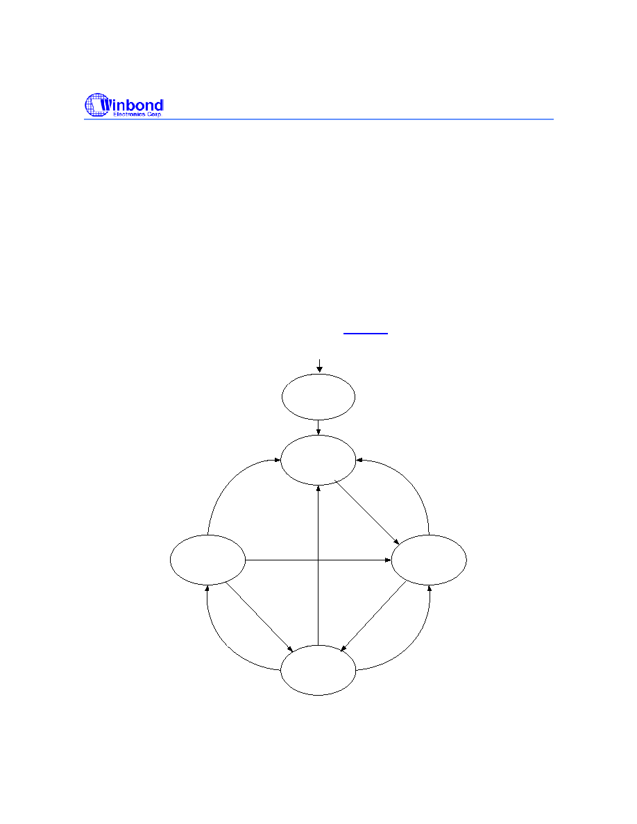
7.4.4 System Operation
The WTS701 is a single chip solution for text-to-speech synthesis. The Text-to-Speech operation is
accomplished by a process of screening the incoming text to normalize common abbreviations and
numbers into a spoken form. The normalized text is then analyzed for phonetic interpretation and this
phonetic translation is mapped into samples to be played out of the analog storage array. This output
signal is then smoothed by a LOW pass filter and is available as an analog signal, or can be passed
through the CODEC for digital audio output.
The WTS701 processor state machine
The WTS701 functions as a state machine and changes states either in response to a command sent
by the host controller, after execution of command is completed, or as a result of an internal event.
The WTS701 states are described below in reference to
Figure 10
.
Vcc Applied
Powe Down
Idle
Wait
Convert
Reset
Soft Reset, PWDN
PWDN, Soft Reset
Soft Reset
PWDN
PWUP
Hard Reset Idle
Convert
Convert
Stop
finish
finish word
conversion finished
Hard Reset
Figure 10. WTS701 Processor States

WTS701
- 42 -
RESET
The WTS701 processor is initialized to the RESET state when Vcc is first applied to the part.
After a reset condition the device enters the POWER DOWN state. All configuration registers are
initialized to their default values after issuing the PWUP command.
Once the WTS701 is active and a hardware reset is applied on the RESET pin, the WTS701 will be in
IDLE state, and all configuration registers will return to their default values.
POWER DOWN
In this state, the power consumption of the WTS701 is minimal. All analog outputs are tristate, the
crystal interface is deactivated and the micro-controller is stopped. The only commands valid in the
Power Down mode are PWUP, SCLC and RDST. All configuration registers will return to their default
values after issuing the PWUP command.
IDLE
The idle state is first entered with the PWUP command. In this state, the micro-controller is running
and the device is ready to respond to further commands. From the IDLE state, the device can go to
the active CONVERT state or the POWER DOWN state.
CONVERT
This state is initiated by the CONV command. The text located in the internal buffer is converted into
speech and played back to the analog or digital interface according to the state of the configuration
registers. Once the active conversion has finished, the device enters the WAIT state.
WAIT
Once a conversion has finished, the device enters the WAIT state. In this state, audio outputs are
still active. To deactivate, audio outputs and return to the IDLE state an IDLE command is issued.

WTS701
Publication Release Date: 6/25/2002
- 43 -
Revision 3.08
7.4.5 Initialization and Configuration
Configuration
After power-on or a Reset command (RST) the WTS701 processor can be configured for operation.
This involves initializing the internal configuration registers for the users requirements.
Table 11. Initialization Commnad Sequence
State
Command
Description
POWER DOWN --------
State after power-on or RST command.
SCLC
Set clock configuration.
PWUP
Power up device.
IDLE
SCOM
Set up communication register to enable interrupts.
SCOD
Set up CODEC configuration (if used).
SAUD
Set up audio control register.
SVOL
Set the initial volume level.
SSPD
Set the initial speech output speed level.
SPTC
Set the initial speech pitch level.
7.4.6 Converting Text
After configuration, the WTS701 is ready for text-to-speech conversion. Because of the real-time
nature of speech, some form of flow control is necessary to inform the host system:
1. When the device is ready for more text data
2. When the device has finished converting text
3. When the device can release the audio interface
The CONVERT state is entered by sending a CONV command along with some textual data. The
WTS701 has an internal 256-byte buffer to accept text data. The R/B\ signal (both the hardware line
and the status bit) will become active (LOW):
1. When the internal buffer is full
2. If the host sends data at a rate too fast for the WTS701 to process it to the internal buffer
When R/B\ becomes active the user may:
1. Wait for the R/B\ pin to return to the (HIGH) ready state
2. Terminate the SPI transaction until a later time and resend the data

WTS701
- 44 -
The user has the choice of enabling interrupts to signal the host when there is free space in the
internal buffer. When all text data has been sent the user must indicate this by:
1. Sending a FIN (Finish) command
2. Sending an EOT (ASCII 0x1A) character as the last byte of a CONV command
(MANDARIN UNICODE 0x00 0x1A)
Once the WTS701 has synthesized the contents of the text buffer, it will enter the WAIT state. In this
state the audio interface is still active. To disable the audio interface and return to the IDLE state an
IDLE command is sent. The WAIT state can be detected either through polling of the CNVT bit or
enabling of the ICNV interrupt. An example of the flow for a conversion is shown in
Figure 11
. The
flow here assumes that the COM register is set such that the WTS701 generates an IBUF interrupt at
the 75 percent buffer level (64 free bytes) and that the ICNV interrupt is enabled.
IDLE
Send CONV
command
Fill serial buffer
with text data
Wait for IBUF
interrupt
Write a new batch
of text data to
buffer ( < 192
bytes otherwise
buffer may
overflow)
Sent all data?
Send FIN
command
Yes
Wait for ICNV
interrupt or
CNVT
cleared
Send IDLE
command
No
Figure 11. Flow Diagram for Convert Operation.

WTS701
Publication Release Date: 6/25/2002
- 45 -
Revision 3.08
Controlling Text Conversion
The WTS701 offers several features to control text conversion. The PAUS (Pause) and RES
(Resume) commands allow the host to pause and then continue speech output. The FINW
command allows the host to end a conversion after the next whole word is spoken. The ST (Stop)
command will terminate a conversion immediately � even mid-word. To allow more advanced
control, the WTS701 allows the host to interrogate the byte count register, which keeps track of the
position in the input stream that is currently being spoken. If the host wishes to repeat a spoken
word, it should:
1. Read the byte count register
2. Send a FINW or ST command
3. Wait for ICNV
4. Send a new CONV command resending the data starting at the desired number of bytes,
according to the repeated spoken words, prior to the count returned in the byte count
In a similar way a skip function could be implemented to skip ahead words or sentences.
7.5 SPI I
NTERFACE
The SPI interface consists of the 4-wire bus SS\, SCLK, MOSI and MISO. In addition flow control
protocols are implemented via the R/B\ signal and/or the WTS701 Status register transmitted via
MOSI. The WTS701 processor also has the option to communicate with the host via interrupt
services requested by the interrupt request line. The timing and behavior of these signals is
dependent upon the command class being executed, i.e., commands with or without associated data.
Additionally the use of the R/B\ hardware control line is not compulsory; rather the host can monitor
the R/B\ bit of the status register to determine when data has been accepted. The status register
also contains the ICMD bit. This bit is set to indicate an SPI transaction has been ignored, indicating
that the WTS701 processor is unable to service a new command. Asynchronous (Class 0)
commands are always accepted. For more information, refer to subsection
7.3.1
which describes the
command classes.
7.5.1 SPI Transactions
SPI Transactions with the WTS701 are broken down into four classes and four basic types:
Type I - Single Word Transactions
Single word transactions are Class 0 or Class 1 commands that have no data to transmit or transmit
all required data in the command data byte. R/B\ will never become active for these commands.
ICMD could be active for a Class 1 command if the WTS701 is still interpreting the previous
command.
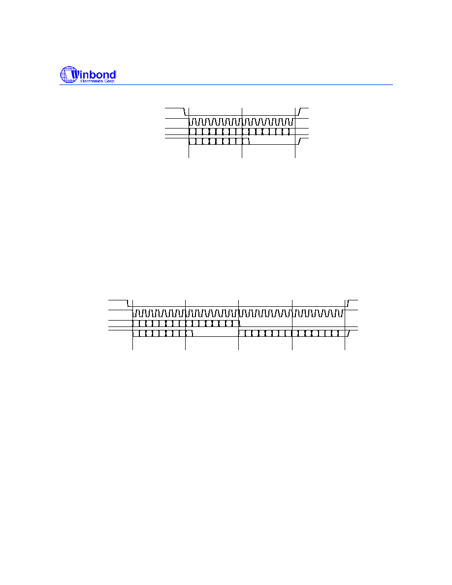
WTS701
- 46 -
0
1
2
3
4
5
6
7
8
9
a
b
c
d
e
f
Command By te
Command
Data By te
0
0
0 0
0
0
0
I
CNT IB
UF
I
ICN
V
CO
D
BF
U
L
BEM
P
CNV
T
RD
Y
R/
B
ICMD
SCLK
MOSI
MISO
SSB
I
ABB
Figure 12. Type I SPI Transaction.
Type II � Two Word Transactions that Receive Data
Type II transactions are four byte transactions that read out the byte count register. As these
commands are all Class0, ICMD will never be active and R/B\ will never occur.
0
1
2
3
4
5
6
7
8
9
a
b
c
d
e
f
Command By te
Command
Data By te
0
0
0 0
0
0
Data By te 0
(ev en)
Data By te 1
(odd)
0
1
2
3
4
5
6
8
9
a
b
c
d
e
f
7
0
ICN
T
IB
UF
I
IC
NV
CO
D
BF
U
L
BE
M
P
CN
V
T
RDY R/
B
IC
MD
SCLK
MOSI
MISO
SSB
BCNT0
BCNT1
IA
B
B
Figure 13. Type II SPI Transaction.
Type III � Transactions that send data
Type III transactions send data to the WTS701. If the data rate exceeds the ability of the WTS701 to
read data from the input FIFO or if the internal data queue becomes full then the R/B\ line will
handshake a pause in the SPI transaction. The host can either:
Wait for R/B\ to return HIGH then continue sending data
Terminate the transaction and try sending data later

WTS701
Publication Release Date: 6/25/2002
- 47 -
Revision 3.08
0
1
2
3
4
5
6
7
8
9
a
b
c
d
e
f
Command By te
Command
Data By te
0
0
0 0
0
0
IC
NT
IB
UF
I
I
CNV CO
D
BF
U
L
BE
M
P
CN
V
T
RDY
R/B
IC
MD
SCLK
MOSI
MISO
SSB
I
ABB
0
SCLK
MOSI
MISO
SSB
0
1
2
3
4
5
6
7
8
9
a
b
c
d
e
f
0
0
0 0
0
0
1
2
3
4
5
6
7
8
9
a
b
c
d
e
f
Data n+2
(ev en)
Data n+3
(odd)
0
0
0 0
0
0
0
Data n
(ev en)
Data n+1
(odd)
R/B low with SPI End
R/B
0
IC
NT
IB
UFI
IC
NV
CO
D
BF
U
L
BE
M
P
CN
V
T
RD
Y
R/
B
IC
M
D
IC
NT
IB
UFI
IC
NV
CO
D
BF
U
L
BE
M
P
CN
V
T
RD
Y
R/
B
IC
M
D
IA
B
B
IA
B
B
Figure 14. Type III SPI Transaction.
Type IV � Transactions reading data
Type IV transactions read data from the WTS701. Because of the latency required for the WTS701 to
place data in the output register, R/B\ must be monitored.
0
1
2
3
4
5
6
7
8
9
a
b
c
d
e
f
Command By te
Command
Data By te
0
0
0 0
0
0
Data By te 0
(ev en)
Data By te 1
(odd)
0
1
2
3
4
5
6
8
9
a
b
c
d
e
f
7
0
ICN
T
IB
UFI
ICNV CO
D
BF
U
L
BEM
P
CNV
T
RDY R/B
ICMD
SCLK
MOSI
MISO
SSB
R/B
I
ABB
Figure 15. Type IV SPI Transaction.

WTS701
- 48 -
7.6 CODEC I
NTERFACE
The WTS701 processor supports analog and digital telephony in various configurations. The
WTS701 can be used in digital environments, along with a DSP that controls a CODEC. Therefore,
the WTS701 is configured to operate in slave mode, where the control signals are provided by an
external source, which is usually the DSP. It supports a variety of single channel CODECs,
examples of which are listed in
Table 12
.
The CODEC interface is designed to send data in short frame format as well as long frame format.
The channel width is 13 or 16 bits linear, the precision of the output is 10 bits. The operation mode of
the CODEC is configured by the COD configuration register and SCOD command. See subsection
7.4.2
for details.
� The CODEC can be configured to transmit data in the unsigned or 2's Complement mode
(see
Table 13
for details).
� The CODEC responds to both the Long and Short sync format (see
Figure 16
and
Figure 17
).
� The CODEC can be configured to tristate the VDX line after 13 or 16 bits.
Table 12. Supported CODEC Examples.
Manufacturer
CODEC
Device Name
Characteristics
Operating
Voltage
Conversion
Type
Data Format
OKI
ML7041
Single codec
3 V
14-bit linear
2s Complement
OKI
MSM7716
Single codec
3 V
14-bit linear
2s Complement
OKI
MSM7732-011 Single codec
3 V
14-bit linear
2s Complement
Motorola
MC145483
Single codec
3 V
13-bit linear
2's Complement
Lucent
T8538B
Quad codec
3.3 V
16-bit linear
2's Complement

WTS701
Publication Release Date: 6/25/2002
- 49 -
Revision 3.08
Table 13. CODEC Transmission Modes.
Signed Mode (2's Complement)
Unsigned Mode
Level
Sign
Bit
(MSB)
13 Bit Mode
16 Bit Mode
13 Bit Mode
16 Bit Mode
+ve full scale
0
1111 1111 1000 1111 1111 1000 0000 1 1111 1111 1000
1111 1111 1100 0000
+1 LSB
0
0000 0000 1000 0000 0000 1000 0000 1 0000 0000 1000
1000 0000 0100 0000
Zero (ground)
0
0000 0000 0000 0000 0000 0000 0000 1 0000 0000 0000
1000 0000 0000 0000
-1 LSB
1
1111 1111 1000 1111 1111 1000 0000 0 1111 1111 1000
0111 1111 1100 0000
-ve full scale
1
0000 0000 0000 0000 0000 0000 0000 0 0000 0000 0000
0000 0000 0000 0000
13 12 11 10 9 8 7 6
5 4 0 0
VD X
VCLK
VFS
MSB
LSB
0
Figure 16. CODEC Protocol, 13 bit, Short Frame Sync.
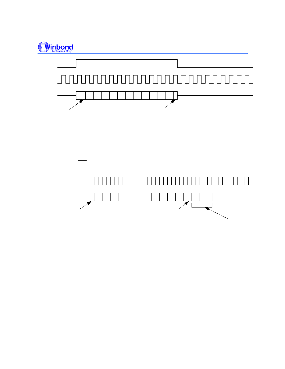
WTS701
- 50 -
13 12 11 10 9 8
7
6 5
4 0
0
VD X
VCLK
VFS
MSB
LSB
0
Figure 17. CODEC Protocol, 13 bit, Long Frame Sync.
4 0 0 0
VD X
VC LK
VFS
0
MSB
LSB
3 ZEROS
10 9 8
7 6
13 12 11
5
0 0
Figure 18. CODEC Protocol, 16 bit, Short Frame Sync.
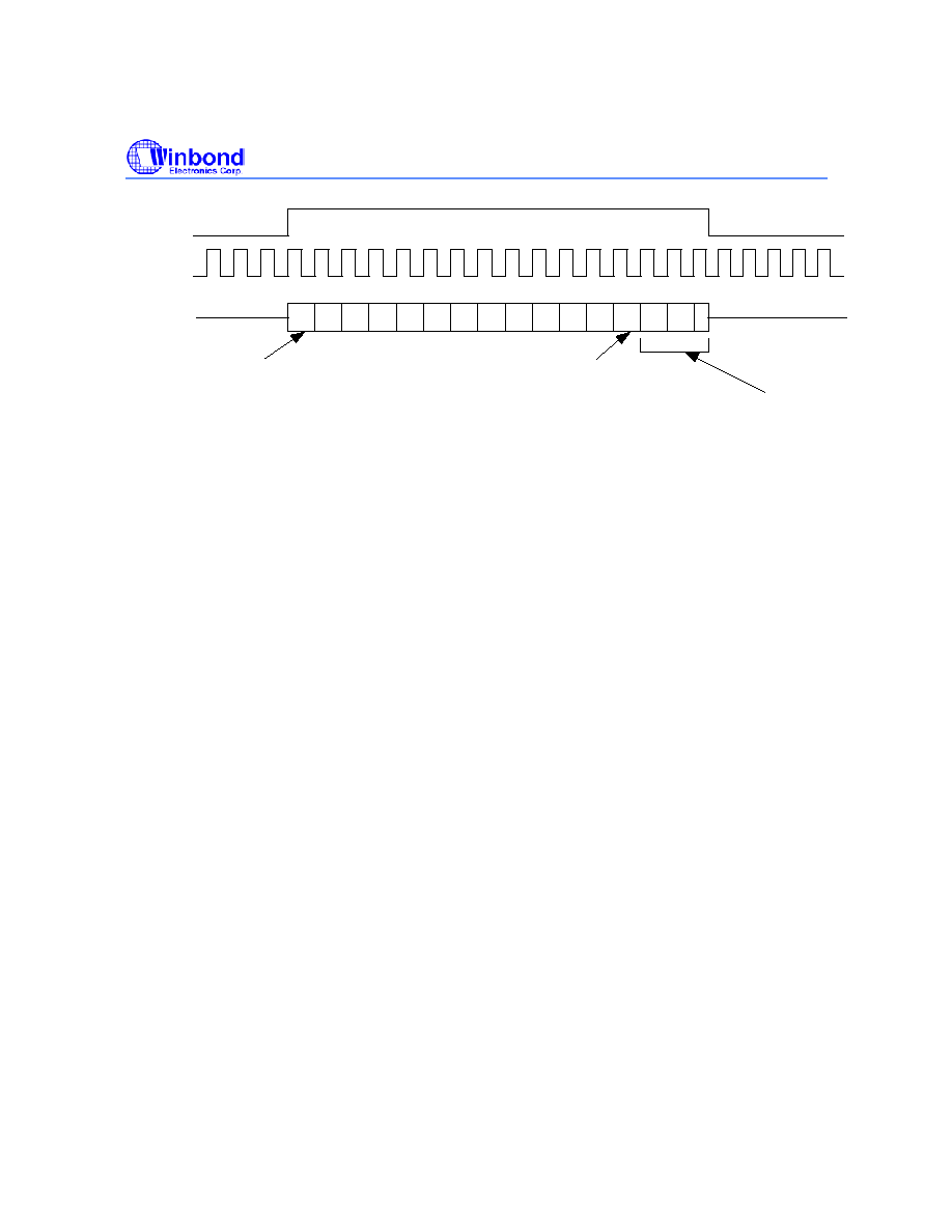
WTS701
Publication Release Date: 6/25/2002
- 51 -
Revision 3.08
4
0 0
0
VD X
VC LK
0
MSB
LSB
3 ZEROS
10 9 8
7 6
13 12 11
5
0
0
VFS
Figure 19. CODEC Protocol, 16 bit, Long Frame Sync.
7.7
PHONETIC ALPHABET PLAYBACK
The WTS701 uses an intermediate phonetic translation represented as an alphabet that represents
phonemes and stress for each input word. This feature allows the text sent to the WTS701 to be
consisted of a combination of ASCII characters as well as phonetic alphabet. This capability offers the
flexibility to send words already processed for phonetic representation, achieving the desired
pronunciation.
Phonetic strings can be sent directly to the WTS701. This can be done by embedding phoneme
strings in the text stream for conversion. To embed a phoneme string, the string must be preceded by
a control-P (^P, ASCII 0x10) character and terminated by a space character.
For example:
"The quick ^Pbr1Wn fox."
The following table lists the phoneme symbols acceptable by the WTS701E (English software
version). As the acceptable phoneme symbols are language dependent, please refer to the specific
language User's Guide for details regarding characters accepted and other development
considerations.

WTS701
- 52 -
Table 14. Acceptable Phoneme Symbols.
Vowels Consonants
Phoneme Example
Phoneme Example
i
beat p
pet
I bit t
t
en
e bait k
k
it
E bet b
b
et
@ bat d
d
ebt
u boot g
g
et
U book h
h
at
o boat f
f
at
c bought T thing
a Bob D
th
at
A but s
s
at
R burr S
sh
ut
O boy v
v
at
Y buy z
z
oo
W down Z
azure
x
a
bout y
y
ou
X roses w
w
it
r rent
l let
m met
n net
G sing
C church
J judge
Note that each phoneme is represented by exactly one character and each vowel is preceded by a
pitch symbol
.

WTS701
Publication Release Date: 6/25/2002
- 53 -
Revision 3.08
Numbers 1 and 0 represent stress: each word has a single 1 stress, representing the main stress of
the word; all other syllables have 0 stress.
Examples:
Input Phonetic
translation
hi.
h1Y (phoneme /h/, followed by a 1-stress vowel phoneme Y)
test
t1Est
testing
t1Est0IG
7.8
CUSTOMIZING ABBREVIATIONS
The WTS701 has support for entering and using custom abbreviations in addition to the general
abbreviation table supported internally by the WTS701. There are 2K bytes of flash memory
reserved for this purpose. After the WTS701 internal software has been initially programmed, this
entire area is free and available for custom abbreviations.
The commands associated with custom abbreviations are:
Command Command
Byte
Command
Data Byte
ABBR_ADD 0xaf
0x00
+
abbreviation
data.
Adds a new abbreviation to the
abbreviation table in the WTS701
See next page for the format of
the abbreviation data.
ABBR_DEL 0x83
0x00+
abbreviation
data.
Deletes an existing abbreviation
from the abbreviation table in the
WTS701. See next page for the
format of the abbreviation data.
ABBR_NUM
0xc8
0x00 + 0x00
+ 0x00.
Returns the number of
abbreviation currently active in the
abbreviation table of the WTS701.
ABBR_MEM
0xc7
0x00 + 0x00
+ 0x00.
Returns the number of free bytes
in the abbreviation table of the
WTS701.
ABBR_RD
0xc9
0x00 + 2048
0x00s.
Returns the abbreviation table
contents from the WTS701. See
next page for the format of the
abbreviation table data.
ENTER_RRSM 0x0c 0x00
Causes the xdata and code store
memory to swap spaces. The
WTS701 begins to execute code
previously stored into xdata after
this command.

WTS701
- 54 -
7.8.1 Abbreviation Data Format
The format of the abbreviation data that is sent with the ABBR_ADD and ABBR_DEL commands is:
XXX + "," + YYYY + ";".
XXX - the abbreviation characters.
"," � comma.
YYYY � abbreviation text.
";" � semi-colon.
Example: TTS,text to speech; After this is added using the ABBR_ADD command, when the text
"TTS" is sent as part of the convert data, the WTS701 will speak "text to speech" instead of T T S.
Note: when deleting an abbreviation, the abbreviation text is optional.
To delete the TTS example, only "TTS,;" is necessary.
7.8.2 Abbreviation Table Format
The format of the abbreviation table returned with the ABBR_RD command is:
Abbreviation entry - Marker + Count + XXX + 0x00 + YYYY + 0x00.
Marker � The marker will be either 0xfe for active abbreviation or 0xfc for a deleted abbreviation.
Count � The byte count for this entry including the Marker, Count, XXX, YYYY, and zeros.
XXX � the abbreviation characters.
0x00 � Null terminator.
YYYY � abbreviation text.
0x00 � Null terminator.
The unused data are always 0xff.

WTS701
Publication Release Date: 6/25/2002
- 55 -
Revision 3.08
7.8.3 Command Execution
ABBR_NUM & ABBR_MEM - These commands are executed by sending the command and
command data, waiting for R/B\ to be ready, then receiving two bytes from MISO. The first byte
received is the MSB, and the second is LSB.
ABBR_RD � This command is executed by sending the command and command data, waiting for
R/B\ to be ready, then receiving 2048 characters (the entire abbreviation table).
ABBR_ADD & ABBR_DEL � These commands are executed by sending the command and command
data, followed by the abbreviation data formatted as described in subsection
7.8.1
. When the
WTS701 is ready for the next step, it will generate an IABB interrupt. After the interrupt, send the
ENTER_RSSM (0x0c + 0x00) command. After issuing the command wait for 100mS. After the
timeout, the WTS701 will have programmed the new abbreviation entry and be ready to accept more
commands. Adding or removing an abbreviation will reset the configuration registers to their default
values.
After abbreviation entry deletion, the abbreviation entry is only deleted from the table and not used,
however it still holds memory space. The only way to free all memory will be to reprogram the
WTS701 internal software into the device.
7.9
D
EVICE
P
ROGRAMMING
The WTS701 is fully programmable to support different languages or different voices that can be
loaded to the device whenever the user wishes to do so. The language or the voice module should
be stored externally and transmitted to the WTS701 processor with regards to a specific protocol
defined in this section.
Programming the WTS701 consists of downloading a binary executable to the processor code
memory and a digitized analog speech corpus to the non-volatile analog multi-level storage (MLS).
Winbond will supply code as a set of ASCII readable data files, the information will be provided to
qualified customers upon request.

WTS701
- 56 -
7.10 T
EXT
-
TO
-
SPEECH PROCESSOR COMMMANDS
�
QUICK REFERENCE TABLE
.
Status Commands
Command
Description
Opcode Hex
Previous
State
Result
State
Command
Parameters
Return
Value
Name
Class
T
y
pe
Command
byte
Command
data
Description
Bytes
Description
RDST 0 II Read
Status 04 00
Idle, Convert,
Power Down
No change
None -
Byte
count
RINT 0 II Read
Interrupt
06 00
Idle, Convert
No change
None -
Byte
count
RVER 0 II Read
version
12 00
Idle, Convert
No change
None -
Hw_ver,
Sw_ver

WTS701
Publication Release Date: 6/25/2002
- 57 -
Revision 3.08
System Commands
Command
Description
Opcode Hex
Previous
State
Result
State
Command
Parameters
Return Value
Name
Class
Type
Command
byte
Command
data
Description
By
tes
Description
By
tes
PWUP
0 I Exit Power
Down mode
02 00
Power
Down
Idle None
-
None -
PWDN
1 I Go
To
Power
Down mode
40 00
Idle,
Convert
Wait
Power
Down
None - None -
RST
0 I Reset
10 00
Idle,
Convert
Wait, Power
down
Power
Down
None - None -

WTS701
- 58 -
Synthesis Commands
Command
Description
Opcode Hex
Previous
State
Result
State
Command
Parameters
Return Value
Name
Class
Type
Command
byte
Command
data
Description
By
tes
Description
By
tes
CONV 2
III
Convert text
81
00
Idle, Wait
Convert
Text
data
N None -
PAUS 1 I Pause
conversion
49 00
Convert No
change
None -
None -
RES 1 I Resume
conversion
4A 00
Convert No
change
None -
None -
ST 1
I
Stop
conversion
4B 00
Convert Wait
None -
None -
FINW 1 I Finish
word 4D 00
Convert Wait
None -
None -
FIN 1 I Finish
4C 00
Convert Wait
None -
None -
VLUP 1 I Volume
up 53
00
Idle,
Convert
Wait
No
change
None -
None -
VLDN 1 I Volume
down 54
00
Idle,
Convert
Wait
No
change
None -
None -
SPUP 1 I Speed
up
55
00
Idle,
Convert
Wait
No
change
None -
None -
SPDN 1 I Speed
down 56
00
Idle,
Convert
Wait
No
change
None -
None -
IDLE 1 I Switch
to
Idle
state
57 00
Wait,
Convert
Idle None -
None -

WTS701
Publication Release Date: 6/25/2002
- 59 -
Revision 3.08
Configuration Commands
Command
Description
Opcode Hex
Previous
State
Result
State
Command
Parameter
s
Return
Value
Name
Class
Type
Command
byte
Command
data
Description
By
tes
Description
RREG 3 IV Read
configuration
register
C0
Register
Number
Idle,
Convert
No
change
None - Registe
r value,
dummy
byte
SCOM 1 I Set COM
register
4E Value
Idle, Wait
No
Change
None - None
SCOD 1 I Set COD
register
4F Value
Idle, Wait
No
Change
None - None
SAUD 1 I Set AUD
register
50 Value
Idle, Wait
No
Change
None - None
SVOL 1 I Set VOL
register
51 Value
Idle, Wait
No
Change
None - None
SSPD 1 I Set SPD
register
52 Value
Idle, Wait
No
Change
None - None
SCLC 1 I Set CLC
register
14 Value
Idle, Wait
No
Change
None - None
SPTC 1 I Set
Speech
Pitch
77 Value
Idle, Wait
No
Change
None - None

WTS701
- 60 -
Customization Commands
Command
Description
Opcode Hex
Previous
state
Result
State
Command
Parameters
Return
Value
Name
Class
Type
Command
byte
Command
data
Description
B
y
tes
Description
ABBR_
NUM
3 IV
Return
number of
abbreviation
entries
C8 00 Idle
No
change
None -
Num_of_entries
ABBR_
RD
3 IV
Read
abbreviation
table
C9
00
Idle
No
change
None -
Abbreviation
table entries
ABBR_
MEM
3 IV
Return
abbreviation
memory
C7 00 Idle
No
change
None -
Available_mem
ABBR_
ADD
2 III
Add
abbreviation
AF 00 Idle
No
change
Abbreviation
information
N None
ABBR_
DEL
1 I Delete
abbreviation
entry
83 00 Idle
No
change
Abbreviation
information
N None
ENTER
_RRS
M
0 I Swap
memory
0C 00 Idle
No
change
None -
None

WTS701
Publication Release Date: 6/25/2002
- 61 -
Revision 3.08
7.10.1 Text Input Format
The following table lists the ASCII characters acceptable by the WTS701E (English software version).
Please refer to the specific language User's Guide for more details regarding characters accepted and
other development considerations.
Table 15. Allowable ASCII Characters.
0x0
0x20
space
0x40 0x60
0x1
0x21
!
0x41
A
0x61
a
0x2
0x22 0x42 B 0x62 b
0x3
0x23
#
0x43
C
0x63
c
0x4
0x24 $ 0x44 D 0x64 d
0x5
0x25
%
0x45
E
0x65
e
0x6
0x26
&
0x46
F
0x66
f
0x7
0x27
`
(apostrophe)
0x47 G 0x67 g
0x8
0x28 0x48 H 0x68 h
0x9
0x29 0x49 I 0x69 I
0xa
0x2a
*
0x4a
J
0x6a
j
0xb
0x2b
+
0x4b
K
0x6b
k
0xc
0x2c
,
(comma)
0x4c
L
0x6c
l
0xd
0x2d
-
(dash)
0x4d M 0x6d m
0xe
0x2e
.
(period, dot) 0x4e N 0x6e n
0xf
0x2f
/
0x4f
O
0x6f
o
0x10 Enable
phonetic
alphabet
0x30 0 0x50 P 0x70 p
0x11 0x31 1 0x51 Q 0x71 q
0x12
0x32
2
0x52
R
0x72
r
0x13
0x33
3
0x53
S
0x73
s
0x14
0x34
4
0x54
T
0x74
t
0x15 0x35 5 0x55 U 0x75 u
0x16
0x36
6
0x56
V
0x76
v
0x17
0x37
7
0x57
W
0x77
w
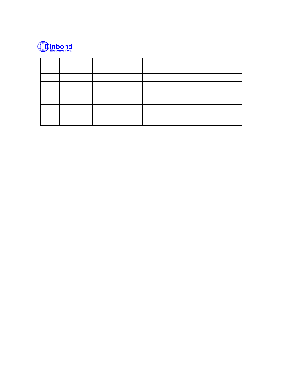
WTS701
- 62 -
0x18
0x38
8
0x58
X
0x78
x
0x19
0x39
9
0x59
Y
0x79
y
0x1a EOT
0x3a
:
(column)
0x5a Z 0x7a z
0x1b 0x3b 0x5b 0x7b
0x1c 0x3c 0x5c \ 0x7c
0x1d 0x3d = 0x5d 0x7d
0x1e 0x3e 0x5e 0x7e
0x1f 0x3f ?
0x5f _
(underscore)
0x7f
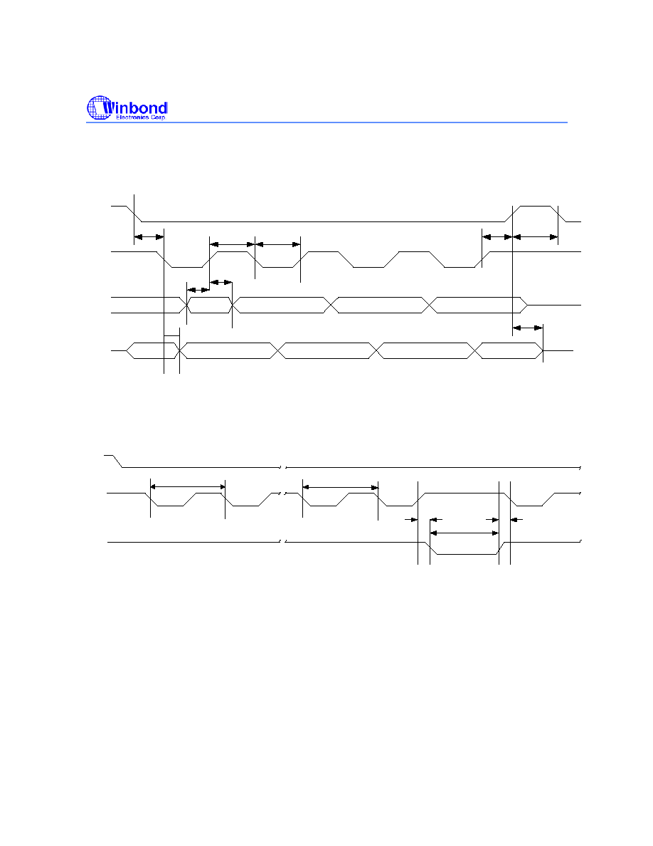
WTS701
Publication Release Date: 6/25/2002
- 63 -
Revision 3.08
8. TIMING WAVEFORMS
8.1 SPI
TIMING DIAGRAM
SSB
SCLK
MOSI
T
s s h
T
dih
T
dis
T
s s s
T
s s m in
T
s c lk high
T
s c lk low
T
df
T
pd
MISO
TRISTA TE
TRISTA TE
Figure 20. SPI Timing Specification.
SSB
SCLK
T
rblow
T
rbh
T
rbd
R/B
BIT 0
BIT 15
Figure 21. SPI R/B\ Timing.
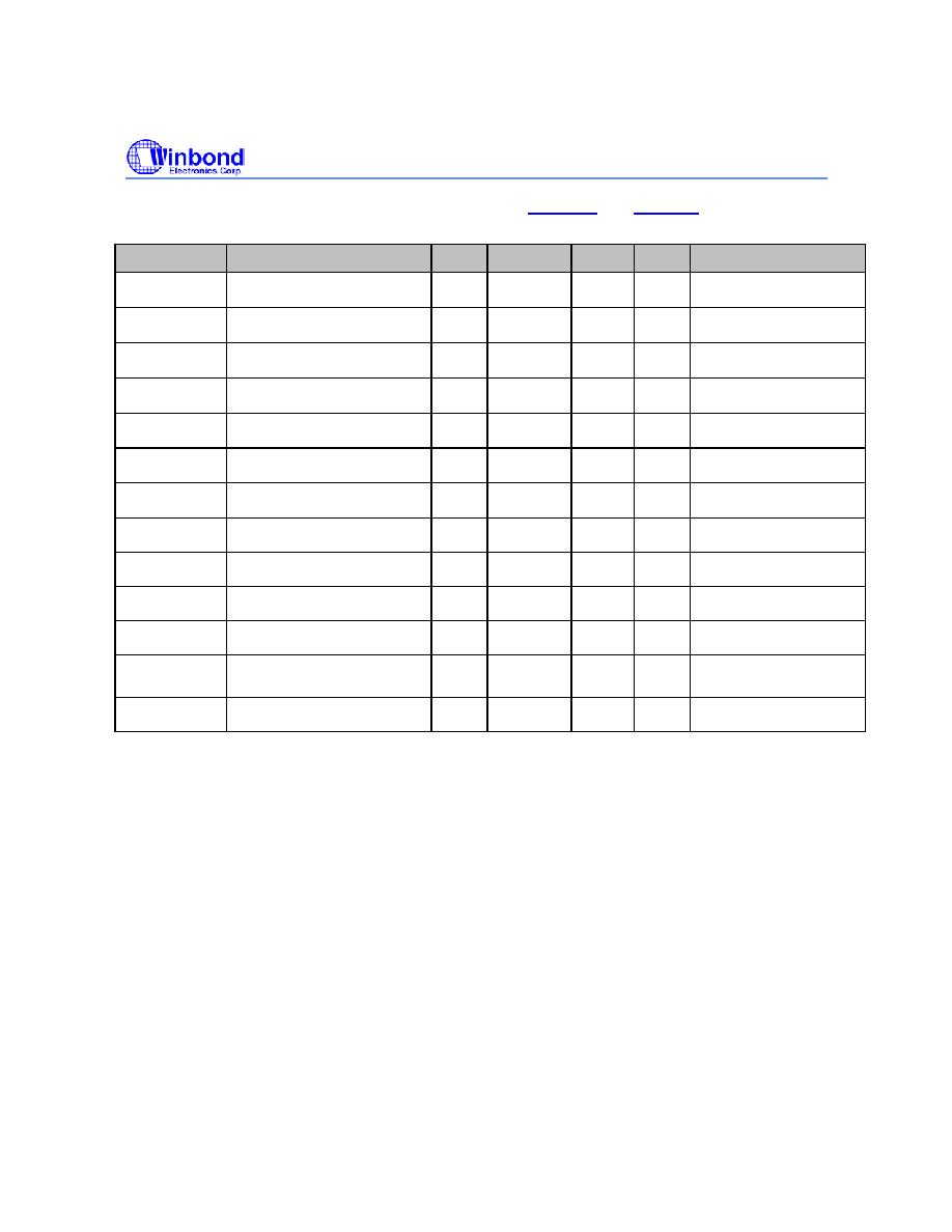
WTS701
- 64 -
Table 16. SPI Timing Parameters (see
Figure 20
and
Figure21
)
Symbol
Parameters
Min
Typ
(7)
Max
Units Conditions
T
SSS
SS\ Setup Time
100
ns
T
SSH
SS\ Hold Time
100
ns
T
DIS
Data in Setup Time
50
ns
T
DIH
Data in Hold Time
50
ns
T
PD
Output
Delay
100
ns
T
DF
Output Delay to hiZ
100
ns
T
SSmin
SS\
High
200
ns
T
SCKhi
SCLK High Time
80
ns
T
SCKlow
SCLK Low Time
80
ns
T
rbd
Delay SCLK Hi to R/B\ low
80
ns
T
rblow
R/B\ low time
0
ms
T
rbh
SCLK hold time from R/B\
High
0
F
O
CLK
Frequency
5000
kHZ
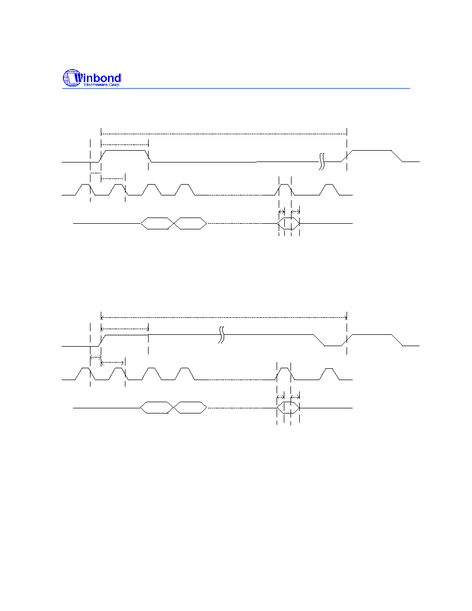
WTS701
Publication Release Date: 6/25/2002
- 65 -
Revision 3.08
8.2 CODEC T
IMING
D
IAGRAMS
MSB
MSB-1
LSB
t
s ync
t
f sp
t
s x
t
x
t
dv
t
dhi
Figure 22. CODEC Timing -- Short Frame Sync.
MSB
MSB-1
LSB
t
s ync
t
f sp
t
s x
t
x
t
dv
t
dhi
Figure 23. CODEC Timing -- Long Frame Sync.
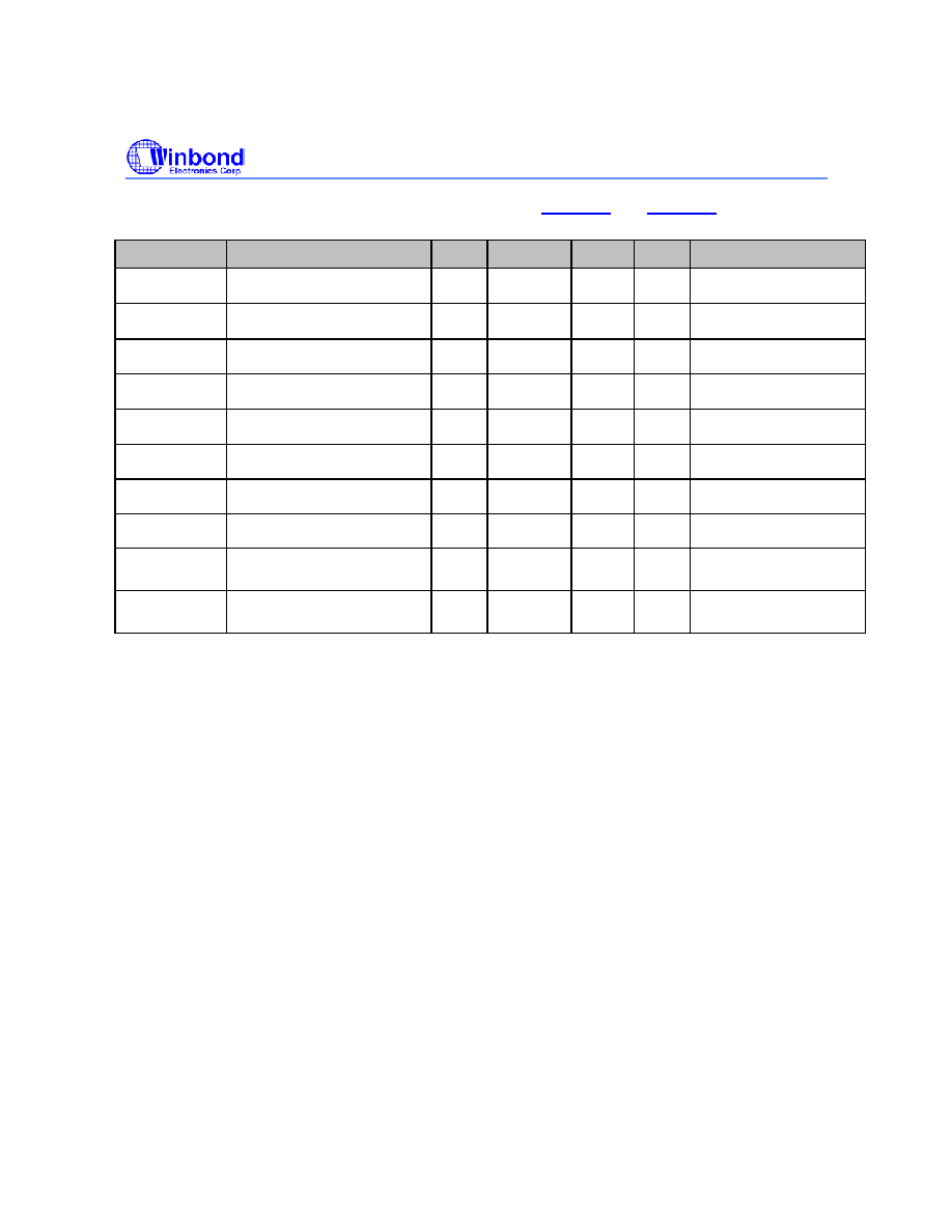
WTS701
- 66 -
Table 17. CODEC Timing Parameters (see
Figure 22
and
Figure 23
)
Symbol
Parameters
Min
Typ
(7)
Max Units Conditions
T
clk
Bit clock frequency
128
2048
kHz
T
sync
Frame. Sync. Frequency
8
kHz
D
C
Clock Duty Cycle
45
50
55
%
T
ir
Rise Time
50
ns
All digital inputs
T
if
Fall Time
50
ns
All digital inputs
T
fsp
Frame Sync. Pulse Width
100
ns
VFS
T
rs
Receive Sync. Timing
20
ns
VCLK to VFS
T
sr
Receive Sync. Timing
80
ns
VFS to VCLK
T
dv
Output Delay Time for VDX
Valid
10
140
ns
VCLK to VDX
T
dhi
Output Delay Time for VDX
High Impedance
10
140
ns
VCLK to VDX
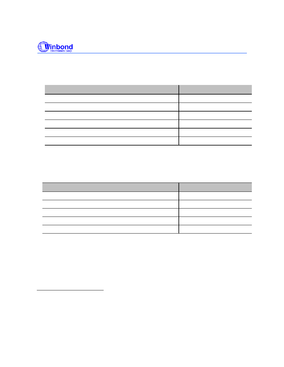
WTS701
Publication Release Date: 6/25/2002
- 67 -
Revision 3.08
9. ABSOLUTE MAXIMUM RATINGS
Table 18. Absolute Maximum Ratings (Packaged Parts)
(1)
Condition
Value
Junction temperature
150
0
C
Storage temperature range
-65
0
C to +150
0
C
Voltage Applied to any pin
(V
SS
- 0.3V) to (V
CC
+ 0.3V)
Voltage applied to any pin (Input current limited to +/-20 mA)
(2)
(V
SS
� 1.0V) to (V
CC
+ 2.2V)
Lead temperature (soldering � 10 seconds)
300
0
C
V
CC
- V
SS
-0.3V to +7.0V
Table 19. Operating Conditions (Packaged Parts).
Condition
Value
Commercial operating temperature range
(3)
0
0
C to +70
0
C
Extended operating temperature
(2)
-20
0
C to +70
0
C
Industrial operating temperature
(2)
-40
0
C to +85
0
C
Supply voltage (V
CC
)
(4)
+2.7V to +3.3V
Ground voltage (V
SS
)
(5)
0V
1
Stresses above those listed may cause permanent damage to the device. Exposure to the absolute maximum
ratings may affect device reliability. Functional operation is not implied at these conditions.
2
All input pins except for CS\ signal, which is 3V tolerant ONLY.
3
Case Temperature.
4
V
CC
= V
CCA
= V
CCD
.
5
V
SS
= V
SSA
= V
SSD

WTS701
- 68 -
10. ELECTRICAL CHARACTERISTICS
(V
CC
= 3.3V, V
SS
= 0V, T
A
= 0 to 70
�C)
Table 20. General Parameters.
PARAMETER SYMBOL
TEST
CONDITIONS
SPEC
UNIT
MIN
(6)
TYP
(7)
MAX.
Input LOW Voltage
V
IL
V
CC
x
0.2
V
Input HIGH Voltage
V
IH
V
CC
x
0.8
V
Output LOW Voltage
V
OL
I
OL
= 10
�A
0.4 V
R/B\, INT\ Output LOW
Voltage
V
OL1
I
OL
= 1 mA
0.4 V
Output HIGH Voltage
V
OH
I
OL
= -10
�A
V
CC
�
0.4
V
V
CC
Current (Operating)
- Convert
- Idle
- CODEC
- Speaker
I
CC
No Load
(8)
No Load
(8)
No Load
(8)
No Load
(8)
50
20
20
15
mA
mA
mA
mA
V
CC
Current (Standby)
I
SB
(8)
50
�A
Input Leakage Current
I
IL
+/-1
�A
6
All Min/Max limits are guaranteed by Winbond via electrical testing or characterization. Not all specifications
are 100% tested.
7
Typical values are T = 25
�C and V
CC
= 3.0V, timing measured at 50% levels.
8
V
CCA
and V
CCD
summed together.

WTS701
Publication Release Date: 6/25/2002
- 69 -
Revision 3.08
Table 21. Speaker Driver Specifications.
PARAMETER SYMBOL
TEST
CONDITIONS
SPEC
UNIT
MIN. TYP. MAX.
SP+/- Output Voltage
(HIGH Gain Setting)
V
SPHG
Peak-to-Peak,
differential
load = 150
3.6 V
SP+/- Output Load Imp.
(LOW Gain)
R
SPLG
8
SP+/- Output Load Imp.
(HIGH Gain)
R
SPHG
70
150
SP+/- Output Load
Cap.
CS\
P
100
pF
SP+/- Output Bias
Voltage (Analog
Ground)
V
SPAG
1.2 V
DC
Speaker Output DC
Offset
V
SPDCO
With AUXIN to Speaker,
AUXIN AC coupled to V
SSA
100
mV
DC
Power Supply Rejection
Ratio
PSRR
Measured with a 1 kHz,
100 ma sine wave input at
V
CC
and V
CC
pins
-55 dB
Frequency Response
(300-3400 Hz)
F
R
With 0TLP input to AUX IN,
6 dB setting
(12)
-0.25 +0.25 dB
Power Output (LOW
Gain Setting)
P
UTLOG
Differential load at 8
23.5
mW
RMS

WTS701
- 70 -
Table 22. AUXOUT Parameters.
PARAMETER SYMBOL
TEST
CONDITIONS
SPEC
UNIT
MIN. TYP. MAX.
AUXOUT � Maximum
Output Swing
V
ANAIUT
5k
Load
1.0 V
Minimum Load
Impedance
R
L
5
k
Maximum Load
Capacitance
C
L
100
pF
AUXOUT V
BIAS
1.2 VDC
Table 23. Volume Control Parameters.
PARAMETER SYMBOL
TEST
CONDITIONS
SPEC
UNIT
MIN. TYP. MAX.
Output Gain
A
OUT
8 steps of 4 dB, referenced
to output
-28
to
0
dB
Absolute Gain
ANA IN 1.0 kHz 0TLP, 6
dB gain setting measured
differentially at SP+/-
-0.5 +0.5 dB
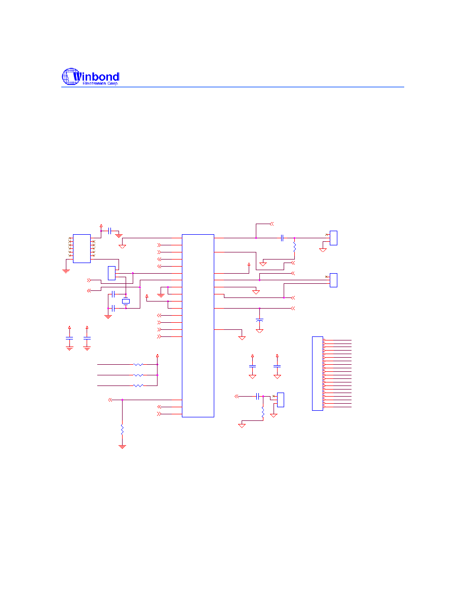
WTS701
Publication Release Date: 6/25/2002
- 71 -
Revision 3.08
11. TYPICAL APPLICATION CIRCUIT
The following schematic diagrams are extracted from the WTS-ES701 evaluation unit, based on the
Winbond WTS-ES701 evaluation board.
The evaluation system includes the following basic clusters:
WTS701 processor cluster working with 3.3V, including an 8-ohm speaker,
SPI connector to the host PC via the PC parallel port.
For more information about the evaluation system, please refer to the WTS-ES701 User's Guide.
PAD_SPK-
PAD_FS
PG 1,3
PAD_RDY
PAD_SPK+
PAD_RESET
PAD_XTO
PG 1
PAD_MOSI
PG 1,3
PAD_MISO
PG 1,3
PAD_XTO
PAD_XTI
PAD_DIN
PAD_AUXOUT
PAD_ATTCAP
PAD_AUXIN
PAD_BCLK
PAD_SCLK
CSB
PAD_XTI
VCCA
PAD_RDY
PAD_BCLK
PG 1,3
PAD_AUXOUT PG 1
PAD_RESET
PG 1,3
PAD_RDY
PG 1,3
PAD_SPK- PG 1
PAD_ATTCAP
PAD_AUXOUT
PAD_INTB
GNDA
PAD_AUXIN
PAD_MOSI
PAD_DIN
PG 1,3
PAD_FS
PAD_SCLK
PG 1,3
PAD_SPK+ PG 1
PAD_XTI
PG 1
PAD_MISO
PAD_INTB
PG 1,3
PAD_INTB
PAD_SSB
PG 1,3
CSB
PG 1
PAD_XTO
VCCD
GND
PAD_SSB
PAD_SPK-
PAD_ATTCAP PG 1
PAD_AUXIN PG 1
PAD_MISO
PAD_SPK+
Y2
XTAL
J2
MJ-3536N
1
2
3
J7
1
2
3
AUXOUT
U5
WTS701
25
15
16
14
6
26
13
8
7
52
40
42
5
4
3
2
36
46
9
10
11
12
27
44
48
54
CSB
SSB
SCLK
MOSI
MISO
RDY
INTB
XTI
XTO
AUXIN
ATTCAP
SPK-
VDX
VFS
VCLK
VSSA1
VSSA2
SPK+
VSSDN
VSSD
VCCD
VCCDN
RESET
VSSA3
VCCA
AUXOUT
R11 33K
C18
10PF
VCCD
U6
CRYSTAL SOCKET
1
2
3
4
5
6
7
8
9
10
11
12
13
14
1
2
3
4
5
6
7
8
9
10
11
12
13
14
C23
.1UF
J4
1
2
3
4
5
6
7
8
9
10
11
12
13
14
15
16
17
18
19
20
C19
10PF
R13
10K
J5
MJ-3536N
1
2
3
C17
.1UF
C25
.1UF
SPEAKER
VCCD
VCCA
C24
.1UF
VCCD
C21
.1UF
VCCD
VCCD
R9 33K
C22
.1UF
R12
33K
+
R8
10K
AUXIN
VCCA
R10 33K
C20
4.7UF
J1
MJ-3536N
1
2
3
Label pins
of J4 with
signal
names.
VCCA
C26
.1UF
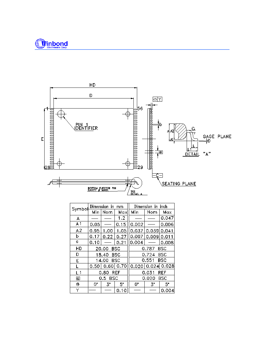
WTS701
- 72 -
12. PACKAGE DRAWING AND DIMENSIONS
56 L TSOP(I) (14X20 MM)
WTS701
Publication Release Date: 6/25/2002
- 73 -
Revision 3.08
13. ORDERING INFORMATION
VERSION
WTS701__ __ /__
Voice
F � Female
M � Male
Language
E � English
M � Mandarin
Package Type
T � TSOP 56-leads
14. VERSION HISTORY
DATE PAGE
DESCRIPTION
3.08
Jun. 2002
1-73
Improved package drawing, added illegal commands description,
modified part number format
3.07
Apr. 2002
1-73
Initial issue
Headquarters
No. 4, Creation Rd. III,
Science-Based Industrial Park,
Hsinchu, Taiwan
TEL: 886-3-5770066
FAX: 886-3-5665577
http://www.winbond.com.tw/
Taipei Office
11F, No. 115, Sec. 3,
Taipei, Taiwan
TEL: 886-2-27190505
FAX: 886-2-27197502
Winbond Electronics Corporation America
2727 North First Street, San Jose,
CA 95134, U.S.A.
TEL: 1-408-9436666
FAX: 1-408-5441798
Winbond Electronics (H.K.) Ltd.
No. 378 Kwun Tong Rd.,
Kowloon, Hong Kong
FAX: 852-27552064
Unit 9-15, 22F, Millennium City,
TEL: 852-27513100
Please note that all data and specifications are subject to change without notice.
All the trade marks of products and companies mentioned in this data sheet belong to their respective owners.
Winbond Electronics (Shanghai) Ltd.
200336 China
FAX: 86-21-62365998
27F, 2299 Yan An W. Rd. Shanghai,
TEL: 86-21-62365999
Winbond Electronics Corporation Japan
Shinyokohama Kohoku-ku,
Yokohama, 222-0033
FAX: 81-45-4781800
7F Daini-ueno BLDG, 3-7-18
TEL: 81-45-4781881
Min-Sheng East. Rd.,