D
3-Terminal Regulators
D
Output Current Up to 100 mA
D
No External Components Required
D
Internal Thermal-Overload Protection
D
Internal Short-Circuit Current Limiting
D
Direct Replacement for Motorola MC79L
Series
description
This series of fixed negative-voltage integrated-circuit
voltage regulators is designed for a wide range of
applications.
These include on-card regulation for
elimination of noise and distribution problems
associated
with single-point regulation. In addition,
they can be used to control series pass elements to make high-current voltage-regulator circuits. One of these
regulators can deliver up to 100 mA of output current. The internal current-limiting and thermal-shutdown features
make them essentially immune to overload. When used as a replacement for a zener-diode and resistor combination,
these devices can provide ef
current.
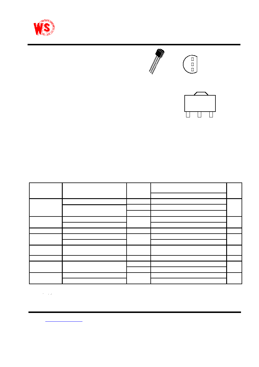
TO≠92
electrical characteristics at specified virtual junction temperature, V
I
=
otherwise noted)
PARAMETER
TEST CONDITIONS
TJ
UNIT
J
MIN
TYP
MAX
V
7 V to 20 V
I
1 mA to 40 mA
25
∞
C
Output voltage
V
7 V t
20 V
I
1
A t 40
A
Full range
V
Full range
Input
VI =
25
∞
C
mV
voltage regulation
VI =
25
∞
C
mV
Ripple rejection
VI =
f = 120 Hz
25
∞
C
49
dB
Output
IO = 1 mA to
25
∞
C
mV
voltage regulation
IO = 1 mA to
25
∞
C
mV
Output
noise voltage
f = 10 Hz to 100 kHz
25
∞
C
µ
V
Dropout voltage
25
∞
C
1.7
V
Bias current
25
∞
C
6
mA
Bias c rrent
125
∞
C
5.5
mA
Bias
VI =
Full range
1.5
mA
current change
IO = 1 mA to 40 mA
F ll range
0.1
mA
Pulse-testing techniques maintain TJ as close to TA as possible. Thermal effects must be taken into account separately. All characteristics are
measured with a 0.33-
µ
F capacitor across the input and a 0.1-
µ
F capacitor across the output. Full range for the 7
J = 0
∞
C to
70∞
C
Wing Shing Computer Components Co., (H.K.)Ltd.
Tel:(852)2341 9276 Fax:(852)2797 8153
Homepage:
http://www.wingshing.com
E-mail:
ic@wingshing.com
79L06
Negative-Voltage Regulators
OUTPUT
INPUT
COMMON
9L06 is T
-5.76
-6
-6.24
-5.7
-6.3
-5.7
-6.3
55
9
16
mV
mA
mA
mV
25 C
25 C
Full
Bias current
I =1 to 70mA, V = -12V to -
-8.5 to -20V
-10V to -20V
-9V to -20V
-9V to -20V
SOT-89
COMMON
INPUT OUTPUT
06
o
20V
fective improvement in output iimpedance of two orders of magnitude, with lower bias
40mA
100mA
45
3
175
125
o
79L06ACZ
79L06CPK
79L06
3-1
11V, I = 40mA (unless
C
O
I
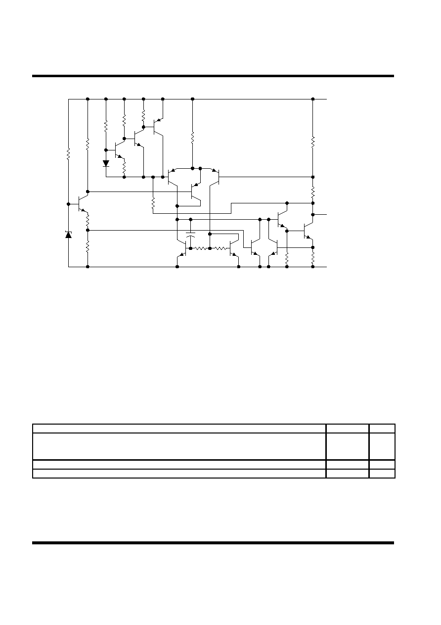
equivalent schematic
OUTPUT
INPUT
COMMON
absolute maximum ratings over operating free-air temperature range (unless otherwise noted)
Input voltage: 79L0
. . . . . . . . . . . . . . . . . . . . . . . . . . . . . . . . . . . . . . . . . . . . . . . . . . . . . . . . . . . . . . . . . . .
Operating free-air, case, or virtual junction temperature
∞
C
. . . . . . . . . . . . . . . . . . . . . . . . . . . . . . . . . . . . . . .
Lead temperature 1.6 mm (1/16 inch) from case for 10 seconds
260
∞
C
. . . . . . . . . . . . . . . . . . . . . . . . . . . . . . .
Storage temperature range, T
stg
≠65
∞
C to 150
∞
C
. . . . . . . . . . . . . . . . . . . . . . . . . . . . . . . . . . . . . . . . . . . . . . . . . . .
recommended operating conditions
MIN
MAX
UNIT
79L0
Input voltage, VI
V
Output current, IO
100
mA
Operating virtual junction temperature, TJ
0
∞
C
WS
79L06
-30V
150
70
6
6
-8 -20
3-2