 | –≠–ª–µ–∫—Ç—Ä–æ–Ω–Ω—ã–π –∫–æ–º–ø–æ–Ω–µ–Ω—Ç: LM386N-1 | –°–∫–∞—á–∞—Ç—å:  PDF PDF  ZIP ZIP |
Low Voltage Audio Power Amplifier
General Description
is a power amplifier designed for use in low volt-
age consumer applications. The gain is internally set to 20 to
keep external part count low, but the addition of an external
resistor and capacitor between pins 1 and 8 will increase the
gain to any value from 20 to 200.
The inputs are ground referenced while the output automati-
cally biases to one-half the supply voltage. The quiescent
power drain is only 24 milliwatts when operating from a 6 volt
supply, making the
Features
n
Battery operation
n
Minimum external parts
n
Wide supply voltage range: 4V≠12V
n
Low quiescent current drain: 4mA
n
Voltage gains from 20 to 200
n
Ground referenced input
n
Self-centering output quiescent voltage
n
Low distortion: 0.2% (A
V
= 20, V
S
= 6V, R
L
= 8
, P
O
=
125mW, f = 1kHz)
n
Available in 8 pin SOP package
Applications
n
AM-FM radio amplifiers
n
Portable tape player amplifiers
n
Intercoms
n
TV sound systems
n
Line drivers
n
Ultrasonic drivers
n
Small servo drivers
n
Power converters
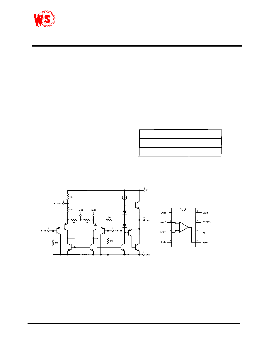
Equivalent Schematic and Connection Diagrams
Small Outline,
Wing Shing Computer Components Co., (H.K.)Ltd.
Tel:(852)2341 9276 Fax:(852)2797 8153
Homepage:
http://www.wingshing.com
E-mail: wsccltd@hkstar.com
Low Voltage
Audio Power Amplifier
WS386M-1 ideal for battery operation
Pin Connection
Dual in Line Package
and DIP package
Ordering Information
PART NO.
PACKAGE
SOP-8
DIP-8
8-1
LM386-1
The LM386-1
LM386M-1
LM386N-1
T
A
= 25∞C
Parameter
Conditions
Min
Typ
Max
Units
Operating Supply Voltage (V
S
)
Quiescent Current (I
Q
)
V
S
= 6V, V
IN
= 0
4
8
mA
Output Power (P
OUT
)
S
= 6V, R
L
= 8
, THD = 10%
250
325
mW
Voltage Gain (A
V
)
V
S
= 6V, f = 1 kHz
26
dB
10 µF from Pin 1 to 8
46
dB
Bandwidth (BW)
V
S
= 6V, Pins 1 and 8 Open
300
kHz
Total Harmonic Distortion (THD)
V
S
= 6V, R
L
= 8
, P
OUT
= 125 mW
0.2
%
f = 1 kHz, Pins 1 and 8 Open
Power Supply Rejection Ratio (PSRR)
V
S
= 6V, f = 1 kHz, C
BYPASS
= 10 µF
50
dB
Pins 1 and 8 Open, Referred to Output
Input Resistance (R
IN
)
50
k
Input Bias Current (I
BIAS
)
V
S
= 6V, Pins 2 and 3 Open
250
nA
Note 1: All voltages are measured with respect to the ground pin, unless otherwise specified.
Note 2: Absolute Maximum Ratings indicate limits beyond which damage to the device may occur. Operating Ratings indicate conditions for which the device is func-
tional, but do not guarantee specific performance limits. Electrical Characteristics state DC and AC electrical specifications under particular test conditions which guar-
antee specific performance limits. This assumes that the device is within the Operating Ratings. Specifications are not guaranteed for parameters where no limit is
given, however, the typical value is a good indication of device performance.
Note 3: For operation in ambient temperatures above 25∞C, the device must be derated based on a 150∞C maximum junction temperature and
a thermal resistance of 170∞C/W for the small outline package.
Absolute Maximum Ratings
Dual-In-Line Package
Soldering (10 sec)
+260∞C
Small Outline Package
(SOIC )
Vapor Phase (60 sec)
+215∞C
Infrared (15 sec)
+220∞C
Electrical Characteristics
(Notes 1, 2)
4
12
V
V
,Vcc=6V,R =8 ,f=1KH , unless otherwise specified
Z
Pins 1 and 8 Open
15V
Soldering Information
Supply Voltage
(WS386-1)
Package Dissipation(Note3)
(WS386N) 1.25W
0.73W
(WS386M)
.4V
+
-
65 C to +150 C
0 C to+70 C
+150 C
Input Voltage
Storage Temperature
Junction Temperature
Operating Temperature
-
8-2
LM386-1
50
0
700
V s = 9V,RL =8 , THD =10%
Bandwidth (BW)
Vs = 6V,10uF from Pin 1 to 8
60
kHz

Application Hints
GAIN CONTROL
a more versatile amplifier, two pins (1
and 8) are provided for gain control. With pins 1 and 8 open
the 1.35 k
resistor sets the gain at 20 (26 dB). If a capacitor
is put from pin 1 to 8, bypassing the 1.35 k
resistor, the
gain will go up to 200 (46 dB). If a resistor is placed in series
with the capacitor, the gain can be set to any value from 20
to 200. Gain control can also be done by capacitively cou-
pling a resistor (or FET) from pin 1 to ground.
Additional external components can be placed in parallel
with the internal feedback resistors to tailor the gain and fre-
quency response for individual applications. For example,
we can compensate poor speaker bass response by fre-
quency shaping the feedback path. This is done with a series
RC from pin 1 to 5 (paralleling the internal 15 k
resistor).
For 6 dB effective bass boost: R
.
15 k
, the lowest value
for good stable operation is R = 10 k
if pin 8 is open. If pins
1 and 8 are bypassed then R as low as 2 k
can be used.
This restriction is because the amplifier is only compensated
for closed-loop gains greater than 9.
INPUT BIASING
The schematic shows that both inputs are biased to ground
with a 50 k
resistor. The base current of the input transis-
tors is about 250 nA, so the inputs are at about 12.5 mV
when left open. If the dc source resistance driving the LM386
is higher than 250 k
it will contribute very little additional
offset (about 2.5 mV at the input, 50 mV at the output). If the
dc source resistance is less than 10 k
, then shorting the
unused input to ground will keep the offset low (about 2.5 mV
at the input, 50 mV at the output). For dc source resistances
between these values we can eliminate excess offset by put-
ting a resistor from the unused input to ground, equal in
value to the dc source resistance. Of course all offset prob-
lems are eliminated if the input is capacitively coupled.
with higher gains (bypassing the
1.35 k
resistor between pins 1 and 8) it is necessary to by-
pass the unused input, preventing degradation of gain and
possible instabilities. This is done with a 0.1 µF capacitor or
a short to ground depending on the dc source resistance on
the driven input.
8
7
6
1
90
5
90
2
4B
Y
3
4A
0
X
1405
Gain
-input
+input
GND
GND
VOUT
V
CC
100
BYPASS
Gain
390
1015
1405
1405
120
7
8
120
120
120
550
600
600
750
440
4A
4B
5
6
2
3
Coordinates
Pad N
Pad Name
X
Y
975
665
100
Chip size 1.4 x 1.6 mm
Pad Location
Pad Location Coordinates
1
8-3
LM386-1
To make LM386-1
When using LM386-1
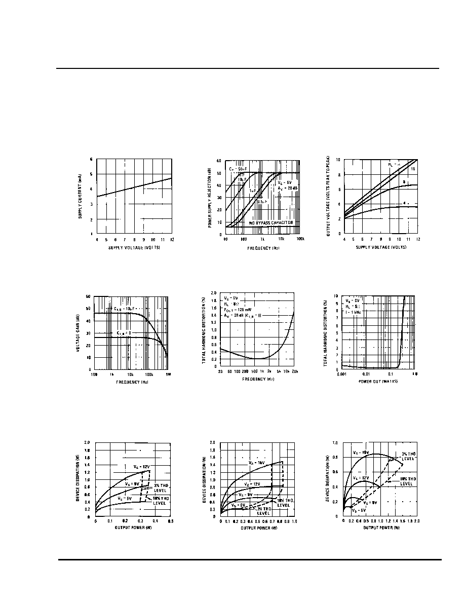
Typical Performance Characteristics
Quiescent Supply Current
vs Supply Voltage
Power Supply Rejection Ratio
(Referred to the Output)
vs Frequency
Peak-to-Peak Output Voltage
Swing vs Supply Voltage
Voltage Gain vs Frequency
Distortion vs Frequency
Distortion vs Output Power
Device Dissipation vs Output
Power -- 4
Load
Device Dissipation vs Output
Power -- 8
Load
Device Dissipation vs Output
Power -- 16
Load
8-4
LM386-1

Typical Applications
Amplifier with Gain = 20
Minimum Parts
Amplifier with Gain = 200
Amplifier with Gain = 50
Low Distortion Power Wienbridge Oscillator
Amplifier with Bass Boost
Square Wave Oscillator
8-5
LM386-1