General Description
consists of two independent precision
voltage comparators with an offset voltage specification as
low as 2.0 mV max for two comparators which were de-
signed specifically to operate from a single power supply
over a wide range of voltages. Operation from split power
supplies is also possible and the low power supply current
drain is independent of the magnitude of the power supply
voltage. These comparators also have a unique characteris-
tic in that the input common-mode voltage range includes
ground, even though operated from a single power supply
voltage.
Application areas include limit comparators, simple analog to
digital converters; pulse, squarewave and time delay gen-
erators; wide range VCO; MOS clock timers; multivibrators
and high voltage digital logic gates. The
designed to directly interface with TTL and CMOS. When op-
erated from both plus and minus power supplies, the
will directly interface with MOS logic where their low
power drain is a distinct advantage over standard compara-
tors.
Advantages
n
High precision comparators
n
Reduced V
OS
drift over temperature
n
Eliminates need for dual supplies
n
Allows sensing near ground
n
Compatible with all forms of logic
n
Power drain suitable for battery operation
Features
n
Wide supply
-- Voltage range:
2.0V to 36V
-- single or dual supplies:
�
1.0V to
�
18V
n
Very low supply current drain (0.4 mA) -- independent
of supply voltage
n
Low input biasing current:
25 nA
n
Low input offset current:
�
5 nA
n
Maximum offset voltage:
�
n
Input common-mode voltage range includes ground
n
Differential input voltage range equal to the power
supply voltage
n
Low output saturation voltage,:
n
Output voltage compatible with TTL, DTL, ECL, MOS
and CMOS logic systems
Wing Shing Computer Components Co., (H.K.)Ltd.
Tel:(852)2341 9276 Fax:(852)2797 8153
Homepage:
http://www.wingshing.com
E-mail: wsccltd@hkstar.com
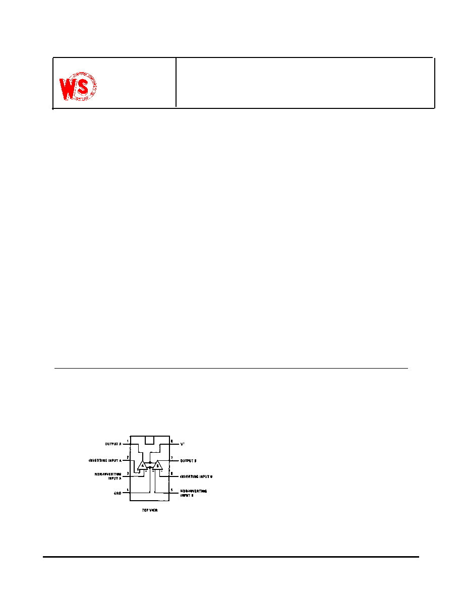
Dual Differential Comparators
Pin Configuration
1
WS393MX
9m V
150 mV at 4 mA
LM393
The LM393
LM393 was
DIP-8
LM393N
SOP-8 LM393M
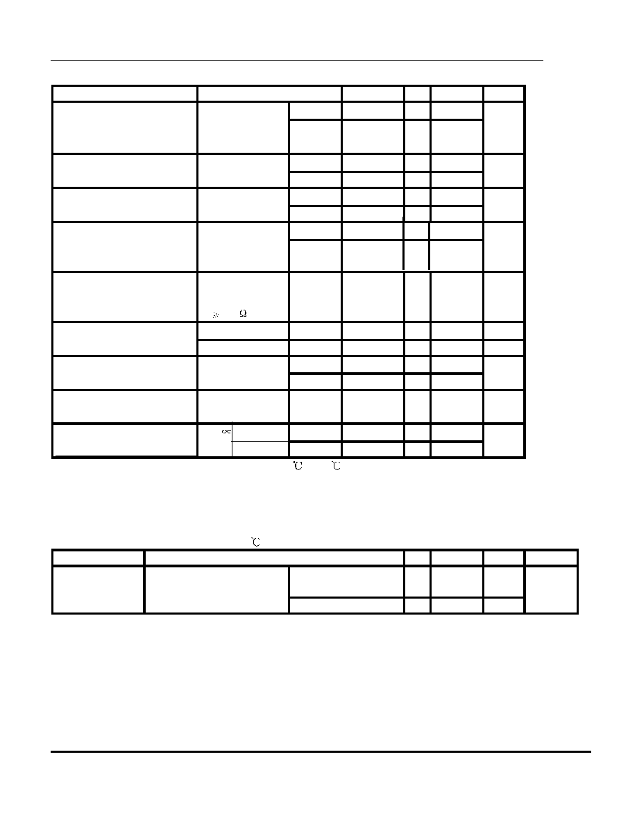
MIN
TYP MAX
UNIT
Vcc = 5V to 30V 25
o
C
2
5
V
IC
= V
ICR
min,
Vo =1.4V
25
o
C
5
50
Full range
150
25
o
C
-25 -250
Full range
-400
25
o
C
Vcc = 15V
Vo =1.4Vto 11.4V
R
L
15k to Vcc
V
OH
=5V,V
ID
=1V 25
o
C
0.1 50
nA
High-level output current
V
OH
=30V,V
ID
=1V Full range
1
u A
25
o
C
150 400
Low-level output voltage
Full range
700
I
OL
Icc
RL= Vcc=5V 25
o
C
0.8 1
Supply current
Vcc=30V Full range
2.5
*Full range(MIN to MAX),for the
LM393 is 0 to 70 .All characteristics are measured with
zero common-mode input voltage unless otherwise speified.
**The voltage at either input or common-mode should not be go negative by more than 0.3V.The upper
end of the common-mode voltage range is Vcc+-1.5V,but either or both inputs can go to 30V without damage
switching characteristics ,Vcc=5V,T
A
=25
PARAMETER
MIN TYP
MAX
UNIT
R
L
connected to 5V
100mV input step with
1.3
us
through 5.1K
5-m V overdrive
CL=15pF see Note1
TTL-level input step
0.3
* CL includes probe and jig capacitance
NOTE1: The response time specified is the interval between the input step function and the instant when
the output crosses 1.4V.
electrical characteristics at specified free-air temperature, Vcc = 4 V (unless otherwise noted)
PARAMETER
TEST CONDITIONS
V
10
input offset voltage
mV
Full range
9
I
IO
Vo =1.4V
nA
input offset current
I
IB
Vo =1.4V
nA
input bias current
V
1CR
0 to Vcc-1.5
V
Common-mode input voltage
Full range 0 to Vcc-2.0
range**
V/m V
Large-signal differential
voltage amplication
A
VD
25
o
C
50
200
I
OH
V
OL
I
OL
=4mA,V
ID
=1V
mV
TEST CONDITIONS
Response time
m A
Low-level output current
m A
V
OL
=1.5V,V
ID
=1V 25
o
C
6
2
LM393
