
General Description
is a highly stable device for generating accurate
time delays or oscillation. Additional terminals are provided
for triggering or resetting if desired. In the time delay mode of
operation, the time is precisely controlled by one external re-
sistor and capacitor. For astable operation as an oscillator,
the free running frequency and duty cycle are accurately
controlled with two external resistors and one capacitor. The
circuit may be triggered and reset on falling waveforms, and
the output circuit can source or sink up to 200mA or drive
TTL circuits.
Features
n
Direct replacement for SE555/NE555
n
Timing from microseconds through hours
n
Operates in both astable and monostable modes
n
Adjustable duty cycle
n
Output can source or sink 200 mA
n
Output and supply TTL compatible
n
Normally on and normally off output
Applications
n
Precision timing
n
Pulse generation
n
Sequential timing
n
Time delay generation
n
Pulse width modulation
n
Pulse position modulation
n
Linear ramp generator
Wing Shing Computer Components Co., (H.K.)Ltd.
Tel:(852)2341 9276 Fax:(852)2797 8153
Homepage:
http://www.wingshing.com
E-mail: wsccltd@hkstar.com
Precision Timer
SO-8
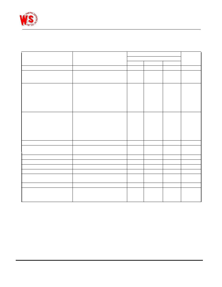
RESET
TRIGGER
VOLTAGE
THRESHOLD
VOLTAGE
OUTPUT
DISCHARGE
SWITCH
Low
High
High
High
Irrelevant
Irrelevant
<1/3V
>1/3V
>1/3V
High
Low
High
On
Off
On
Low
>2/3V
<2/3V
DD
DD
DD
DD
DD
As previously established
FUNCTION TABLE
1
Connection Diagram
NE555
NE555M
DIP-8 NE555N
The NE555
(T
A
= 25�C, V
CC
= +5V to +15V, unless othewise specified)
Parameter
Conditions
Limits
Units
Min
Typ
Max
Supply Voltage
4.5
16
V
Supply Current
V
CC
= 5V, R
L
=
V
CC
= 15V, R
L
=
3
10
6
15
mA
Timing Error, Monostable
Initial Accuracy
1
%
Drift with Temperature
R
A
= 1k to 100k
,
50
ppm/�C
C = 0.1�F, (Note 5)
Accuracy over Temperature
1.5
%
Drift with Supply
0.1
%/V
Timing Error, Astable
Initial Accuracy
2.25
%
Drift with Temperature
R
A
, R
B
= 1k to 100k
,
150
ppm/�C
C = 0.1�F, (Note 5)
Accuracy over Temperature
3.0
%
Drift with Supply
0.30
%/V
Threshold Voltage
0.667
x V
CC
Trigger Voltage
V
CC
= 15V
5
V
V
CC
= 5V
1.67
V
Trigger Current
Reset Voltage
Reset Current
0.1
0.4
mA
Threshold Current
(Note 6)
Control Voltage Level
V
CC
= 15V
V
CC
= 5V
9
2.6
10
3.33
11
4
V
Pin 7 Leakage Output High
1
100
nA
Pin 7 Sat (Note 7)
Output Low
V
CC
= 15V, I
7
= 15mA
180
mV
Output Low
V
CC
= 4.5V, I
7
= 4.5mA
80
200
mV
LM555
ELECTRICAL CHARACTERISTICS
OUTPUT LOW
OUTPUT LOW
Vcc=5V,No load OUTPUT HIGH
2
5
Note 4
0.5
2
uA
0.3
0.7
V
1
Reset at Vcc
30
250
nA
4.5
5.6
1.1
2.2
Trigger at 0V
20
2
3
0.5
NE555

Electrical Characteristics
(Notes 1, 2) (Continued)
(T
A
= 25�C, V
CC
= +5V to +15V, unless othewise specified)
Parameter
Conditions
Limits
Units
Min
Typ
Max
Output Voltage Drop (Low)
V
CC
= 15V
I
SINK
= 10mA
0.1
0.25
V
I
SINK
= 50mA
0.4
0.75
V
I
SINK
= 100mA
2
2.5
V
I
SINK
= 200mA
2.5
V
V
CC
= 5V
I
SINK
= 8mA
V
I
SINK
= 5mA
0.25
0.35
V
Output Voltage Drop (High)
I
SOURCE
= 200mA, V
CC
= 15V
12.5
V
I
SOURCE
= 100mA, V
CC
= 15V
12.75
13.3
V
V
CC
= 5V
2.75
3.3
V
Rise Time of Output
100
ns
Fall Time of Output
100
ns
Note 1: All voltages are measured with respect to the ground pin, unless otherwise specified.
Note 2: Absolute Maximum Ratings indicate limits beyond which damage to the device may occur. Operating Ratings indicate conditions for which the device is func-
tional, but do not guarantee specific performance limits. Electrical Characteristics state DC and AC electrical specifications under particular test conditions which guar-
antee specific performance limits. This assumes that the device is within the Operating Ratings. Specifications are not guaranteed for parameters where no limit is
given, however, the typical value is a good indication of device performance.
Note 3: For operating at elevated temperatures the device must be derated above 25�C based on a +150�C maximum junction temperature and a thermal resistance
170�C/W (S0-8), junction to ambient.
Note 4: Supply current when output high typically
.
Note 5: Tested at V
CC
= 5V and V
CC
= 15V.
Note 6: This will determine the maximum value of R
A
+ R
B
for 15V operation. The maximum total (R
A
+ R
B
) is 20M
.
Note 7: No protection against excessive pin 7 current is necessary providing the package dissipation rating will not be exceeded.
9mA
and MAX. is 13mA at Vcc=15V.
0.15
0.4
0.1
300
300
RECOMMENDED OPERATING
CONDITIONS
MIN
MAX.
UNIT
Supply voltage ,Vcc
Input voltage (control,reset,threshold, and trigger
Output current
Operating free-air temperature, T
A
4.5
16
V
Vcc
+
-
200
mA
0
7
0
C
o
3
)
NE555
0

Applications Information
MONOSTABLE OPERATION
In this mode of operation, the timer functions as a one-shot
(
Figure 1). The external capacitor is initially held discharged
by a transistor inside the timer. Upon application of a nega-
tive trigger pulse of less than 1/3 V
CC
to pin 2, the flip-flop is
set which both releases the short circuit across the capacitor
and drives the output high.
The voltage across the capacitor then increases exponen-
tially for a period of t = 1.1 R
A
C, at the end of which time the
voltage equals 2/3 V
CC
. The comparator then resets the
flip-flop which in turn discharges the capacitor and drives the
output to its low state.
Figure 2 shows the waveforms gener-
ated in this mode of operation. Since the charge and the
threshold level of the comparator are both directly propor-
tional to supply voltage, the timing internal is independent of
supply.
During the timing cycle when the output is high, the further
application of a trigger pulse will not effect the circuit so long
as the trigger input is returned high at least 10�s before the
end of the timing interval. However the circuit can be reset
during this time by the application of a negative pulse to the
reset terminal (pin 4). The output will then remain in the low
state until a trigger pulse is again applied.
When the reset function is not in use, it is recommended that
it be connected to V
CC
to avoid any possibility of false trig-
gering.
Figure 3 is a nomograph for easy determination of R, C val-
ues for various time delays.
NOTE: In monostable operation, the trigger should be driven
high before the end of timing cycle.
ASTABLE OPERATION
If the circuit is connected as shown in
Figure 4 (pins 2 and 6
connected) it will trigger itself and free run as a multivibrator.
The external capacitor charges through R
A
+ R
B
and dis-
charges through R
B
. Thus the duty cycle may be precisely
set by the ratio of these two resistors.
In this mode of operation, the capacitor charges and dis-
charges between 1/3 V
CC
and 2/3 V
CC
. As in the triggered
mode, the charge and discharge times, and therefore the fre-
quency are independent of the supply voltage.
FIGURE 1. Monostable
V
CC
= 5V
Top Trace: Input 5V/Div.
TIME = 0.1 ms/DIV.
Middle Trace: Output 5V/Div.
R
A
= 9.1k
Bottom Trace: Capacitor Voltage 2V/Div.
C = 0.01�F
FIGURE 2. Monostable Waveforms
FIGURE 3. Time Delay
FIGURE 4. Astable
4
NE555

Physical Dimensions
inches (millimeters) unless otherwise noted
5
1
2
3
4
5
6
7
8
95
95
OUTPUT
RESET
THRESHOLD
CONTROL
VOLTAGE
DISCHARGE
Vcc
GND
TRIGGER
Chip Size: 1.02x 1.07 mm
Pad locatin
Pad
N
Pad Name
Coordinates mkm
X
Y
1
2
3
5
4
6
7
8
GND
TRIGGER
OUTPUT
RESET
THRESHOLD
CONTROL VOLTAGE
DISCHARGE
Vcc
95
313
115
126
590
126
810
451
810
635
829
780
420
893
125
492
NE555
NE555M