 | –≠–ª–µ–∫—Ç—Ä–æ–Ω–Ω—ã–π –∫–æ–º–ø–æ–Ω–µ–Ω—Ç: WS7106 | –°–∫–∞—á–∞—Ç—å:  PDF PDF  ZIP ZIP |

Features
∑
∑
∑ Low Noise - Less Than 15
µ
V
P-P
∑
Low Power Dissipation -
Description
are high performance, low
power, 3
1
/
2
digit A/D converters. Included are seven seg-
ment decoders, display drivers, a reference, and a clock.
is designed to interface with a liquid crystal dis-
play (LCD) and includes a multiplexed backplane drive; the
7107 will directly drive an instrument size light emitting
diode (LED) display.
7107 bring together a combination of
high accuracy, versatility, and true economy.
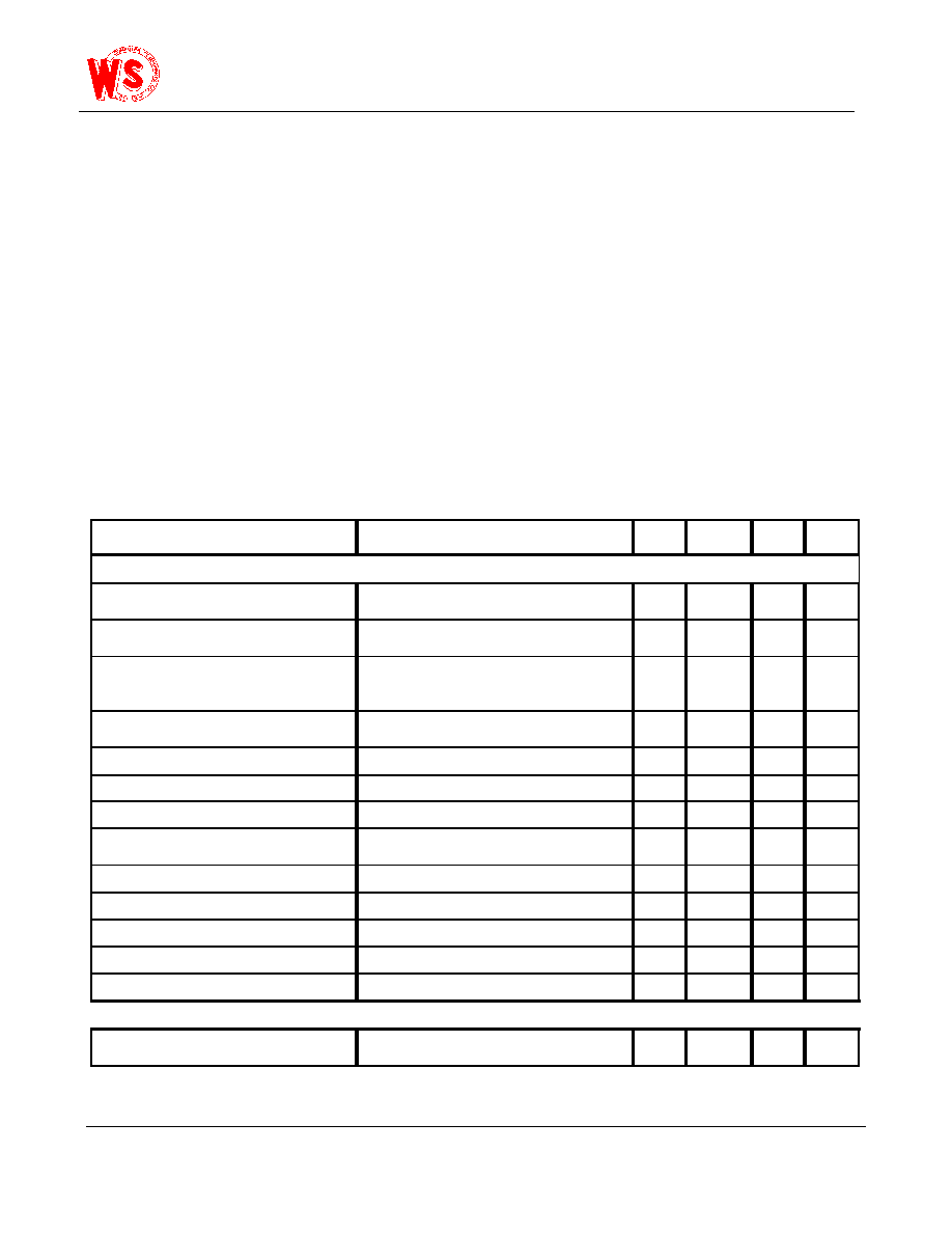
Ordering Information
PART NO.
TEMP.
RANGE (
o
C)
PACKAGE
PKG. NO.
13
1
2
3
4
5
6
7
8
9
10
11
12
14
15
16
17
18
19
20
V+
D1
C1
B1
A1
F1
G1
E1
D2
C2
B2
A2
F2
E2
D3
B3
F3
E3
(1000) AB4
POL
28
40
39
38
37
36
35
34
33
32
31
30
29
27
26
25
24
23
22
21
OSC 1
OSC 2
OSC 3
TEST
REF HI
REF LO
C
REF
+
C
REF
-
COMMON
IN HI
IN LO
A-Z
BUFF
INT
V-
G2 (10' s)
C3
A3
G3
BP/GND
(1' s)
(10' s)
(100' s)
(MINUS)
(100' s)
Wing Shing Computer Components Co., (H.K.)Ltd.
Tel:(852)2341 9276 Fax:(852)2797 8153
Homepage:
http://www.wingshing.com
E-mail: wsccltd@hkstar.com
3 Digit LCD/LED Display A/D
Converters
1
2
/
WS7106 / WS7107
WS7107CPL
0 to70
40Ld PDIP
E40.6
WS7106CPL
0 to 70
40Ld PDIP
E40.6
Pinouts
WS7106CPL (PDIP)
WS7107CPL (PDIP)
- LCD WS7106, LED WS7107
The WS7106 and WS7107
The WS7106
WS
The WS7106 and WS
True differential
inputs and reference are useful in all systems, but give the
desiger an uncommon advantage when measuring load
cells, strain gauges and other bridge type transducers.
Finally, the true economy of single power supply operation
(WS7106), enables a high performance panel meter to built
with the addition of only 10 passive compoents and a disply.
∑ True Differential Input and Reference, Direct Display
Drive
∑ On Chip Clock and Reference
∑ No Additional Active Circuits Required
Guaranteed Zero Reading for 0V Input on All Scales
True Polarity at Zero for Precise Null Detection
Typically Less Than 10mW
Absolute Maximum Ratings
Thermal Information
Supply Voltage
Thermal Resistance (typical, Note 2)
JA
(/W)
WS7106, V+ to V-..................................15v
PDIP Package.................................................... ...... ............ 50
WS7107, V+ to GND...............................6V
Maximum Junction Temperature............................................ .........150
WS7107, V_ to GND......................... ....-9V
Maximum Storage Temperature Range.................................-65 to 150
Analog Input Voltage (Either Input) (Note 1)V+ to V-
Reference Input Voltage (Either Input)V+ to V-
Clock Input
WS7106TEST to V+
WS7107GND to V+
Operating Conditions
Temperature Range..............................0 to 70
CAUTION: Stresses above those listed in "absolute Maximum Ratings" may cause permanent damage to the device. This is a stress only rating and operation
Of the device at these or any other conditions above those indicated in the operational sections of this specification is not implied.
Notes:
1. Input voltages may exceed the supply voltages provided the input current is limited to ±100µA
2.
JA
Is measured with the component mounted on an evaluation PC on board in fee air.
Electrical specifications
(Note 3)
PARAMETER
TEST CONDITIONS
MIN
TYP
MAX
UNIT
SYSTEM PERFORMACE
Zero Input Reading
V
IN
=0.0V, FULL Scale = 200mV
-000.0
±000.0
+000.0
Digital
Reading
Ratiometric Reading
V
IN
= V
REF
, V
REF
= 100mV
999
999/1000
1000
Digital
Reading
Rollover Error
-V
IN
=+V
IN
=200mV
Difference in Reading for Equal Positive and
Negative Inputs Near Full Scale
-1
0.2
+1
Counts
Linearity
Full Scale = 200mV or Full Scale = 2V Maximum
Deviation from Best Straight Line Fit (note 6)
-1
0.2
+1
Counts
Common Mode Rejection Ratio
V
CM
= 1V, V
IN
= 0V, Full Scale = 200mv(Note 6)
-
50
-
V/V
End Power Supply Character V+ Supply Current
V
IN
= 0 (Does Not Include LED Current for WS7107
-
0.5
1.8
mA
End Power Supply Character V- Supply Current
WS7107 Only
-
0.5
1.8
mA
COMMON Pin Analog Common Voltage
25k Between Common and Positive Supply (With
Respect to + Supply)
2.4
3.0
3.2
V
Noise (P
K
-P
K
Value not exceeded 95% of time)
V
IN
=0V Full Scale=200mV
15
uV
P-P
Input Leakage Current
V
IN
=0V
1
10
pA
Analog COMMON Temperature Coefficient
25K between Common and V+ 0-70
60
75
ppm/
Scale Factor Temperature Coefficient
V
IN
=199mV 0-70Ext. ref. 0ppm/
60
75
ppm/
Zero Reading Drift
V
IN
=0V-70
0.2
1
uV/
DISPL
AY DRIVER
WS7106 ONLY
Peak-to-Peak Segment Drive Voltage
Peak-to-Peak Backplane Drive Voltage
V+ = to V- = 9V (Note 5)
4
5
6
V
2
WS7106/WS710
7
Typical Applications and Test Circuits
Segment Sinking Current
V+ = 5V, Segment Voltage = 3V
(Except Pins 19 and 20)
5
8
-
mA
Pin 19 Only
10
16
-
mA
Pin 20 Only
4
7
-
mA
NOTES:
3. Dissipation rating assumes device is mounted with all leads soldered to printed circuit board.
Electrical Specifications
(Continued)
PARAMETER
TEST CONDITIONS
MIN
TYP
MAX
UNIT
7106 TEST CIRCUIT AND TYPICAL APPLICATION WITH LCD DISPLAY COMPONENTS SELECTED FOR 200mV
FULL SCALE
7107 TEST CIRCUIT AND TYPICAL APPLICATION WITH LED DISPLAY COMPONENTS SELECTED FOR 200mV
FULL SCALE
13
1
2
3
4
5
6
7
8
9
10
11
12
14
15
16
17
18
19
20
28
40
39
38
37
36
35
34
33
32
31
30
29
27
26
25
24
23
22
21
V+
D1
C1
B1
A1
F1
G1
E1
D2
C2
B2
A2
F2
E2
D3
B3
F3
E3
AB4
POL
OSC 1
OSC 2
OSC 3
TEST
REF HI
REF LO
C
REF
+
C
REF
-
COM
IN HI
IN LO
A-Z
B
UFF
INT
V-
G2
C3
A3
G3
BP
DISPLAY
DISPLAY
C
1
C
2
C
3
C
4
R
3
R
1
R
4
C
5
+
-
IN
R
5
R
2
9V
C
1
= 0.1
µ
F
C
2
= 0.47
µ
F
C
3
= 0.22
µ
F
C
4
= 100pF
C
5
= 0.02
µ
F
R
1
= 24k
R
2
= 47k
R
3
= 100k
R
4
= 1k
R
5
= 1M
+
-
13
1
2
3
4
5
6
7
8
9
10
11
12
14
15
16
17
18
19
20
28
40
39
38
37
36
35
34
33
32
31
30
29
27
26
25
24
23
22
21
V+
D1
C1
B1
A1
F1
G1
E1
D2
C2
B2
A2
F2
E2
D3
B3
F3
E3
AB4
POL
OSC 1
OSC 2
OSC 3
TEST
REF HI
REF LO
C
REF
+
C
REF
-
COM
IN HI
IN LO
A-Z
B
UFF
INT
V-
G2
C3
A3
G3
GND
DISPLAY
DISPLAY
C
1
C
2
C
3
C
4
R
3
R
1
R
4
C
5
+
-
IN
R
5
R
2
+5V
-5V
C
1
= 0.1
µ
F
C
2
= 0.47
µ
F
C
3
= 0.22
µ
F
C
4
= 100pF
C
5
= 0.02
µ
F
R
1
= 24k
R
2
= 47k
R
3
= 100k
R
4
= 1k
R
5
= 1M
WS7106 / WS7107
WS7107 ONLY
2. Back plane drive is in phase with segment drive for 'off' segment, 180 degrees out of phase for 'on' segment. Frequency is 20
times conversion rate. Average DC component is less than 50mV
WS7106
WS7107
FIGURE 1. WS
FIGURE 2. WS
3
DISPLAY DRIVER
(Note 1)
1.
3. Not tested, Quaranteed by design.
Typical Integrator Amplifier Output Waveform (INT Pin)
Design Information Summary Sheet
∑ OSCILLATOR FREQUENCY
f
OSC
= 0.45/RC
C
OSC
> 50pF; R
OSC
> 50k
f
OSC
(Typ) = 48kHz
∑ OSCILLATOR PERIOD
t
OSC
= RC/0.45
∑ INTEGRATION CLOCK FREQUENCY
f
CLOCK
= f
OSC
/4
∑ INTEGRATION PERIOD
t
INT
= 1000 x (4/f
OSC
)
∑ 60/50Hz REJECTION CRITERION
t
INT
/t
60Hz
or t
lNT
/t
60Hz
= Integer
∑ OPTIMUM INTEGRATION CURRENT
I
INT
= 4
µ
A
∑ FULL SCALE ANALOG INPUT VOLTAGE
V
lNFS
(Typ) = 200mV or 2V
∑ INTEGRATE RESISTOR
∑ INTEGRATE CAPACITOR
∑ INTEGRATOR OUTPUT VOLTAGE SWING
∑ V
INT
MAXIMUM SWING:
(V- + 0.5V) < V
INT
< (V+ - 0.5V), V
INT
(Typ) = 2V
∑ DISPLAY COUNT
∑ CONVERSION CYCLE
t
CYC
= t
CL0CK
x 4000
t
CYC
= t
OSC
x 16,000
when f
OSC
= 48kHz; t
CYC
= 333ms
∑ COMMON MODE INPUT VOLTAGE
(V- + 1V) < V
lN
< (V+ - 0.5V)
∑ AUTO-ZERO CAPACITOR
0.01
µ
F < C
AZ
< 1
µ
F
∑ REFERENCE CAPACITOR
0.1
µ
F < C
REF
< 1
µ
F
∑ V
COM
Biased between Vi and V-.
∑ V
COM
V+ - 2.8V
Regulation lost when V+ to V- <
6.8V
If V
COM
is externally pulled down to (V+ to V-)/2,
the V
COM
circuit will turn off.
7106 POWER SUPPLY: SINGLE 9V
V+ - V- = 9V
Digital supply is generated internally
V
GND
V+ - 4.5V
∑
Type: Direct drive with digital logic supply amplitude.
∑
V+ = +5V to GND
V- = -5V to GND
Digital Logic and LED driver supply V+ to GND
∑
Type: Non-Multiplexed Common Anode
R
INT
V
INFS
I
INT
-----------------
=
C
INT
t
INT
(
)
I
INT
(
)
V
INT
--------------------------------
=
V
INT
t
INT
(
)
I
INT
(
)
C
INT
--------------------------------
=
COUNT
1000
V
IN
V
REF
---------------
◊
=
AUTO ZERO PHASE
(COUNTS)
2999 - 1000
SIGNAL INTEGRATE
PHASE FIXED
1000 COUNTS
DE-INTEGRATE PHASE
0 - 1999 COUNTS
TOTAL CONVERSION TIME = 4000 x t
CLOCK
= 16,000 x t
OSC
WS7106 / WS7107
WS
WS7106 DISPLAY: LCD
WS7107 POWER SUPPLY: DUAL +5.0V
_
WS7107 DISPLAY: LED
4
Detailed Description
Analog Section
Figure 3 shows the Analog Section for the
7107. Each measurement cycle is divided into three
phases. They are (1) auto-zero (A-Z), (2) signal integrate
(INT) and (3) de-integrate (DE).
Auto-Zer o Phase
During auto-zero three things happen. First, input high and
low are disconnected from the pins and internally shorted to
analog COMMON. Second, the reference capacitor is
charged to the reference voltage. Third, a feedback loop is
closed around the system to charge the auto-zero capacitor
C
AZ
to compensate for offset voltages in the buffer amplifier,
integrator, and comparator. Since the comparator is included
in the loop, the A-Z accuracy is limited only by the noise of
the system. In any case, the offset referred to the input is
less than 10
µ
V.
Signal Integrate Phase
During signal integrate, the auto-zero loop is opened, the
internal short is removed, and the internal input high and low
are connected to the external pins. The converter then
integrates the differential voltage between IN HI and IN LO
for a fixed time. This differential voltage can be within a wide
common mode range: up to 1V from either supply. If, on the
other hand, the input signal has no return with respect to the
converter power supply, IN LO can be tied to analog
COMMON to establish the correct common mode voltage. At
the end of this phase, the polarity of the integrated signal is
determined.
De-Integrate Phase
The final phase is de-integrate, or reference integrate. Input
low is internally connected to analog COMMON and input
high is connected across the previously charged reference
capacitor. Circuitry within the chip ensures that the capacitor
will be connected with the correct polarity to cause the
integrator output to return to zero. The time required for the
output to return to zero is proportional to the input signal.
Specifically the digital reading displayed is:
.
Differential Input
The input can accept differential voltages anywhere within the
common mode range of the input amplifier, or specifically from
0.5V below the positive supply to 1V above the negative sup-
ply. In this range, the system has a CMRR of 86dB typical.
However, care must be exercised to assure the integrator out-
put does not saturate. A worst case condition would be a large
positive common mode voltage with a near full scale negative
differential input voltage. The negative input signal drives the
integrator positive when most of its swing has been used up
by the positive common mode voltage. For these critical appli-
cations the integrator output swing can be reduced to less
than the recommended 2V full scale swing with little loss of
accuracy. The integrator output can swing to within 0.3V of
either supply without loss of linearity.
DISPLAY COUNT = 1000
V
IN
V
REF
---------------
FIGURE 3. ANALOG SECTION OF
DE
-
DE+
C
INT
C
AZ
R
INT
BUFFER
A-Z
INT
-
+
A-Z
COMPARATOR
IN HI
COMMON
IN LO
31
32
30
DE-
DE+
INT
A-Z
34
C
REF
+
36
REF HI
C
REF
REF LO
35
A-Z
A-Z
33
C
REF
-
28
29
27
TO
DIGITAL
SECTION
A-Z AND DE
(±)
INTEGRATOR
INT
STRAY
STRAY
V+
10
µ
A
V-
N
INPUT
HIGH
2.8V
6.2V
V+
1
INPUT
LOW
-
+
-
+
-
+
WS7106 / WS7107
WS7106 and
WS
WS7106 AND WS7107
5