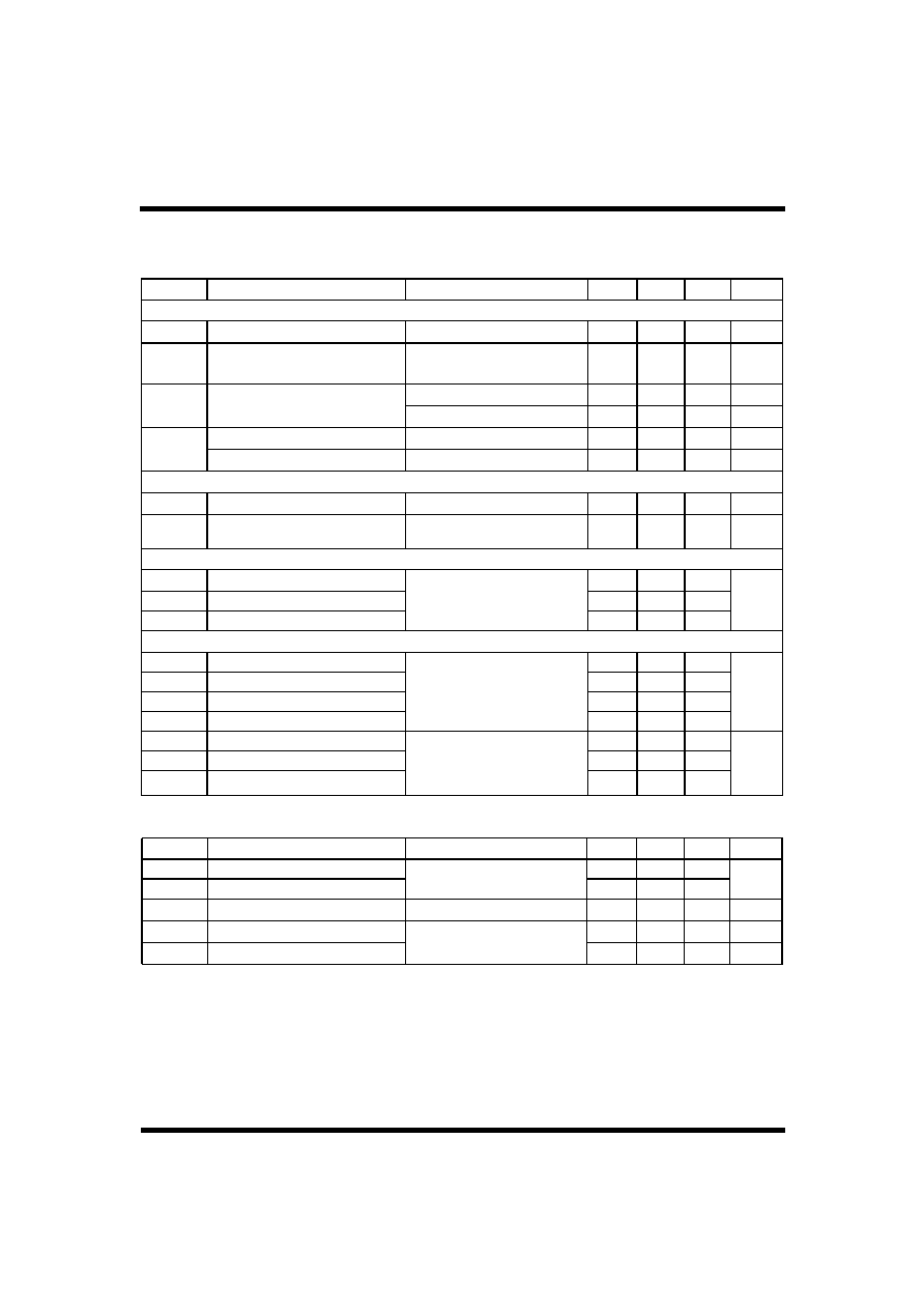
Absolute Maximum Ratings
Symbol
Parameter
Value
Units
V
DSS
Drain to Source Voltage
900
V
I
D
Continuous Drain Current(@T
C
= 25
∞C)
9.0
A
Continuous Drain Current(@T
C
= 100
∞C)
5.7
A
I
DM
Drain Current Pulsed
(Note 1)
36.0
A
V
GS
Gate to Source Voltage
±
30
V
E
AS
Single Pulsed Avalanche Energy
(Note 2)
986
mJ
E
AR
Repetitive Avalanche Energy
(Note 1)
26
mJ
dv/dt
Peak Diode Recovery dv/dt
(Note 3)
4.0
V/ns
P
D
Total Power Dissipation(@T
C
= 25 ∞C)
260
W
Derating Factor above 25 ∞C
2.08
W/∞C
T
STG,
T
J
Operating Junction Temperature & Storage Temperature
- 55 ~ 150
∞C
T
L
Maximum Lead Temperature for soldering purpose,
1/8 from Case for 5 seconds.
300
∞C
Thermal Characteristics
Symbol
Parameter
Value
Units
Min.
Typ.
Max.
R
JC
Thermal Resistance, Junction-to-Case
-
-
0.48
∞C/W
R
CS
Thermal Resistance, Case to Sink
-
0.24
-
∞C/W
R
JA
Thermal Resistance, Junction-to-Ambient
-
-
40
∞C/W
WFW9N90
1/2
Features
R
DS(on)
(Max 1.3
)@V
GS
=10V
Gate Charge
(Typical 55nC)
Improved dv/dt Capability, High Ruggedness
100% Avalanche Tested
Maximum Junction Temperature Range
(150∞C)
General Description
This Power MOSFET is produced using Wisdom's advanced
planar stripe, DMOS technology. This latest technology has been
especially designed to minimize on-state resistance, have a high
rugged avalanche characteristics. These devices are well suited
for high efficiency switch mode power supplies.
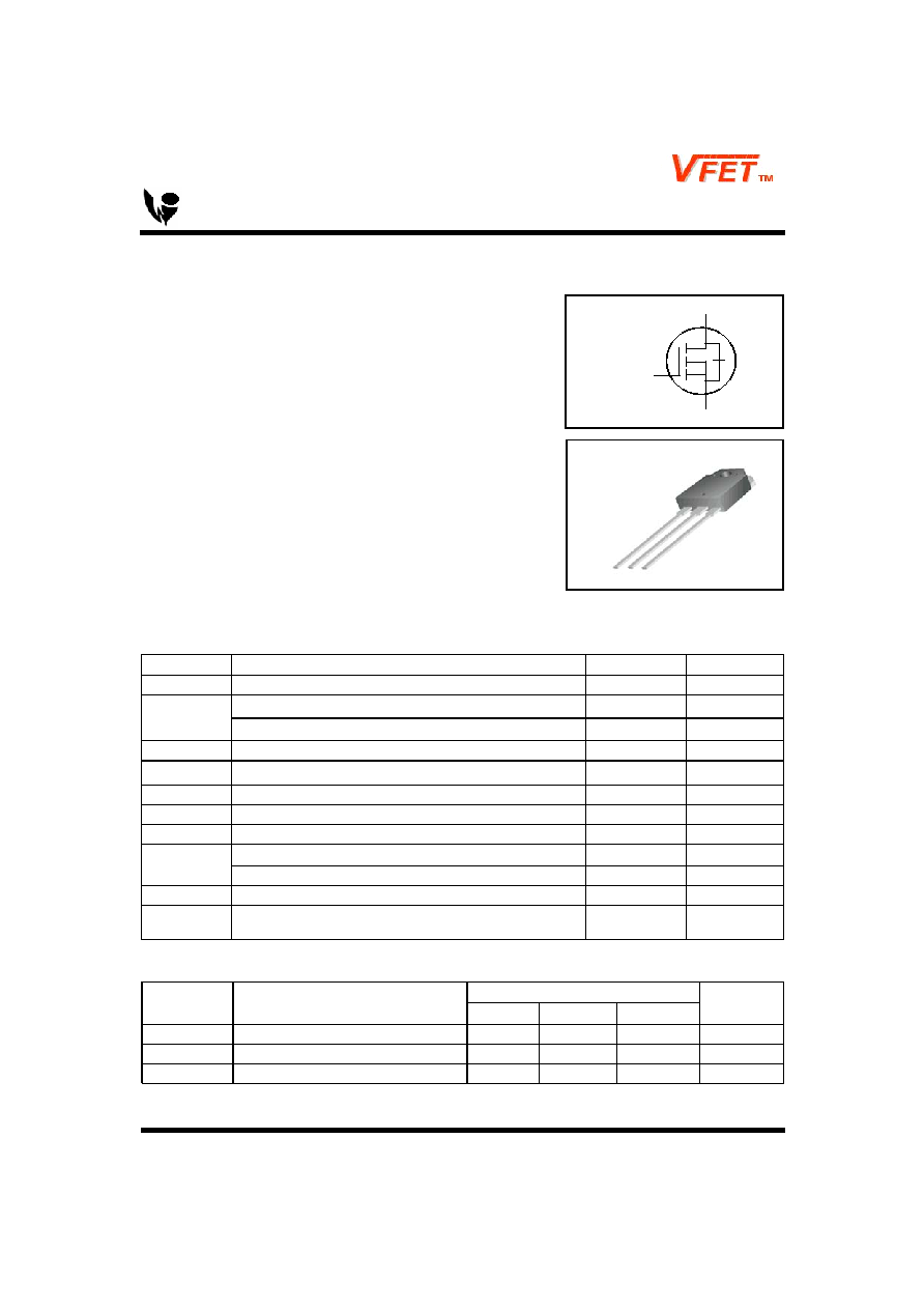
N-Channel MOSFET
Wisdom
Semiconductor
Copyright@Wisdom Semiconductor Inc., All rights reserved.
Symbol
2. Drain
3. Source
1. Gate
PROVISIONAL
TO-247
G
S
D
Electrical Characteristics
( T
C
= 25 ∞C unless otherwise noted )
Symbol
Parameter
Test Conditions
Min
Typ
Max
Units
Off Characteristics
BV
DSS
Drain-Source Breakdown Voltage
V
GS
= 0V, I
D
= 250uA
900
-
-
V
BV
DSS
/
T
J
Breakdown Voltage Temperature
coefficient
I
D
= 250uA, referenced to 25 ∞C
-
1.00
-
V/∞C
I
DSS
Drain-Source Leakage Current
V
DS
= 900V, V
GS
= 0V
-
-
10
uA
V
DS
= 720V, T
C
= 125 ∞C
-
-
100
uA
I
GSS
Gate-Source Leakage, Forward
V
GS
= 30V, V
DS
= 0V
-
-
100
nA
Gate-source Leakage, Reverse
V
GS
= -30V, V
DS
= 0V
-
-
-100
nA
On Characteristics
V
GS(th)
Gate Threshold Voltage
V
DS
= V
GS
, I
D
= 250uA
3.0
-
5.0
V
R
DS(ON)
Static Drain-Source On-state Resis-
tance
V
GS
=10 V, I
D
= 4.5A
-
1.05
1.3
Dynamic Characteristics
C
iss
Input Capacitance
V
GS
=0 V, V
DS
=25V, f = 1MHz
-
2100
-
pF
C
oss
Output Capacitance
-
200
-
C
rss
Reverse Transfer Capacitance
-
25
-
Dynamic Characteristics
t
d(on)
Turn-on Delay Time
V
DD
=450V, I
D
=9.0A, R
G
=25
(Note 4, 5)
-
50
-
ns
t
r
Rise Time
-
100
-
t
d(off)
Turn-off Delay Time
-
140
-
t
f
Fall Time
-
80
-
Q
g
Total Gate Charge
V
DS
=720V, V
GS
=10V, I
D
=9.0A
(Note 4, 5)
-
55
-
nC
Q
gs
Gate-Source Charge
-
15
-
Q
gd
Gate-Drain Charge(Miller Charge)
-
25
-
Source-Drain Diode Ratings and Characteristics
Symbol
Parameter
Test Conditions
Min.
Typ.
Max.
Unit.
I
S
Continuous Source Current
Integral Reverse p-n Junction
Diode in the MOSFET
-
-
9.0
A
I
SM
Pulsed Source Current
-
-
36.0
V
SD
Diode Forward Voltage
I
S
=9.0A, V
GS
=0V
-
-
1.4
V
t
rr
Reverse Recovery Time
I
S
=9.0A, V
GS
=0V, dI
F
/dt=100A/us
-
750
-
ns
Q
rr
Reverse Recovery Charge
-
7.5
-
uC
WFW9N90
NOTES
1. Repeativity rating : pulse width limited by junction temperature
2. L = 23mH, I
AS
=9.0A, V
DD
= 50V, R
G
= 25
, Starting T
J
=
25∞C
3. I
SD
9.0A, di/dt
200A/us, V
DD
BV
DSS
, Starting T
J
=
25∞C
4. Pulse Test : Pulse Width
300us, Duty Cycle
2%
5. Essentially independent of operating temperature.
2/2
Copyright@Wisdom Semiconductor Inc., All rights reserved.