This document contains information on a new product.
Specifications and information are subject to change without notice
WJ Communications, Inc
∑ Phone 1-800-WJ1-4401 ∑ FAX: 408-577-6621 ∑ e-mail: sales@wj.com ∑ Web site: www.wj.com
October
2003
The Communications Edge
TM
AH114
º Watt, High Linearity InGaP HBT Amplifier
Advanced Data Sheet
Product Features
∑
400 ≠ 2500 MHz
∑
+23 dBm P1dB
∑
+40 dBm Output IP3
∑
19 dB Gain @ 900 MHz
∑
14.5 dB Gain @ 1900 MHz
∑
Single Positive Supply (+5V)
∑
SOT-89 SMT Package
Product Description
The AH114 is a high dynamic range driver amplifier in a
low-cost surface mount package. The InGaP/GaAs HBT
is able to achieve high performance across a broad range
with +41 dBm OIP3 and +23 dBm of compressed 1dB
power. It is housed in an industry standard SOT-89 SMT
package. All devices are 100% RF and DC tested.
The AH114 is targeted for use as a driver amplifier in
wireless infrastructure or CATV applications where high
linearity and medium power is required. An internal
active bias allows the AH114 to maintain high linearity
over temperature and operate directly off a single +5 V
supply. This combination makes the device an excellent
candidate for transceiver line cards in current and next
generation multi-carrier 3G base stations.
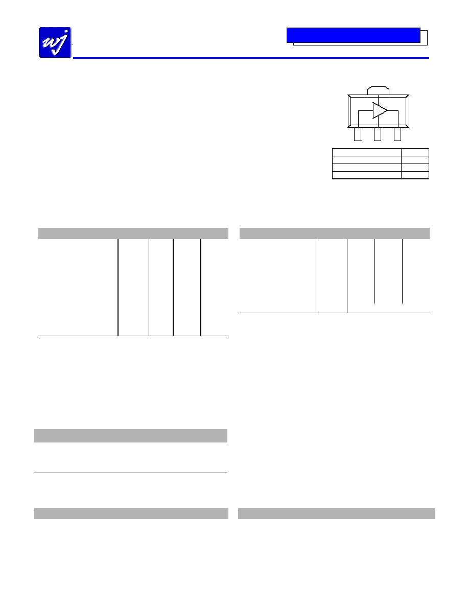
Functional Diagram
1
3
2
4
Function Pin
No.
Input / Base
1
Output / Collector
3
Ground 2,
4
Target Specifications
Parameters
Units Min Typ
Max
Frequency
Range
MHz 400 1900 2500
S21 - Gain
dB
13.5
14.5
S11 - Input R.L.
dB
-10
S22 - Output R.L.
dB
-15
Output P1dB
dBm
+23
Output IP3
dBm
+41
IS-95 Channel Power
@ -60 dBc ACPR
dBm +15
Noise Figure
dB
5.0
Operating Current Range
mA
135
150
165
Device Voltage
V
+5
Test conditions unless otherwise noted.
1. T = 25∫C, Vsupply = +5 V, Frequency = 1900 MHz, in recommended application circuit.
2. 3OIP measured with two tones at an output power of +11 dBm/tone separated by 1 MHz.
The suppression on the largest IM3 product is used to calculate the 3OIP using a 2:1 rule.
Typical Performance
Parameters
Units
Typical
Frequency
MHz
900
1900
2140
S21 - Gain
dB
19
14.5
14.0
S11 - Input R.L.
dB
-10
-10
-15
S22 - Output R.L.
dB
-10
-15
-15
Output
P1dB
dBm +24 +23 +23
Output IP3
2
dBm +40 +41 +40
Noise
Figure
dB 5.0 5.0 6.0
Supply Bias
+5 V @ 150 mA
Typical parameters reflect performance in an application circuit:
Supply Voltage = +5 V, I = 150 mA, +25
∞ C
Thermal Information
Parameters
Rating
Operating Case Temperature
-40 to +85
∞C
Storage Temperature
-55 to +150
∞C
Thermal Resistance
149
∞C/W
Absolute Maximum Rating
Ordering Information
Parameters
Rating
Part No.
Description
Operating Case Temperature
-40 to +85
∞C
AH114
º Watt, High Linearity InGaP HBT Amplifier
Storage Temperature
-65 to +150
∞C
AH114-PCB900
900 MHz Evaluation Board
RF Input Power (continuous)
+12 dBm
AH114-PCB1900 1900 MHz Evaluation Board
Device Voltage / Current
+6 V / 220mA
AH114-PCB2140 2140 MHz Evaluation Board
Operation of this device above any of these parameters may cause permanent damage.

This document contains information on a new product.
Specifications and information are subject to change without notice
WJ Communications, Inc
∑ Phone 1-800-WJ1-4401 ∑ FAX: 408-577-6621 ∑ e-mail: sales@wj.com ∑ Web site: www.wj.com
October
2003
The Communications Edge
TM
AH114
º Watt, High Linearity InGaP HBT Amplifier
Advanced Data Sheet
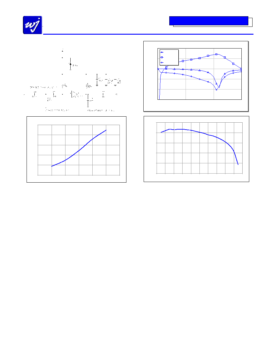
900 MHz Application Circuit
1900 MHz Application Circuit
AH114- IP3 Vs Pout @ 900 MHz
35
37
39
41
43
45
-1
1
3
5
7
9
11
13
15
17
19
Pout/tone
IP3
AH114- IP3 Vs Pout @ 1900 MHz
33
35
37
39
41
43
45
-1
1
3
5
7
9
11
13
15
17
19
Pout/tone
IP3
ACPR IS-95A 9 Channels Forward @ 900 MHz
885KHz Offset/30KHz BW ACPR
-80
-70
-60
-50
-40
5
10
15
20
Channel Power (dBm)
dBc
0
500
1000
1500
2000
Frequency (MHz)
Application Circuit: 900 MHz
-20
-10
0
10
20
30
dB
DB(|S[1,1]|) *
DB(|S[2,1]|) *
DB(|S[2,2]|) *
0
1000
2000
3000
Frequency (MHz)
Application Circuit: 1900 MHz
-20
-10
0
10
20
30
dB
DB(|S[1,1]|) *
DB(|S[2,1]|) *
DB(|S[2,2]|) *
ACPR IS-95A 9 Channels Forward @ 1900 MHz
885KHz Offset/30KHz BW ACPR
-80
-70
-60
-50
-40
5
10
15
20
Channel Power (dBm)
dBc
This document contains information on a new product.
Specifications and information are subject to change without notice
WJ Communications, Inc
∑ Phone 1-800-WJ1-4401 ∑ FAX: 408-577-6621 ∑ e-mail: sales@wj.com ∑ Web site: www.wj.com
October
2003
The Communications Edge
TM
AH114
º Watt, High Linearity InGaP HBT Amplifier
Advanced Data Sheet
2140 MHz Application Circuit
AH114- IP3 Vs Pout @ 2.14 GHz
33
35
37
39
41
43
-1
1
3
5
7
9
11
13
15
17
19
Pout/tone
IP3
ACPR W-CDMA Test Model 1 + 64 DPCH @ 2140 MHz
5MHz Offset/3.84MHz BW ACPR
-60
-55
-50
-45
-40
-35
12
13
14
15
16
17
18
Channel Power (dBm)
dBc
0
1000
2000
3000
Frequency (MHz)
Application Circuit: 2140 MHz
-30
-20
-10
0
10
20
dB
DB(|S[1,1]|) *
DB(|S[2,1]|) *
DB(|S[2,2]|) *

This document contains information on a new product.
Specifications and information are subject to change without notice
WJ Communications, Inc
∑ Phone 1-800-WJ1-4401 ∑ FAX: 408-577-6621 ∑ e-mail: sales@wj.com ∑ Web site: www.wj.com
October
2003
The Communications Edge
TM
AH114
º Watt, High Linearity InGaP HBT Amplifier
Advanced Data Sheet
Outline Drawing
Land Pattern
Product Marking
The component will be marked with an "AH114"
designator with a four- or five-digit alphanumeric lot
code on the top surface of the package. Tape and reel
specification for this part is located on the website in
the "Application Notes" section.
ESD / MSL Information
ESD Classification: Class 1A
Test:
Human Body Model (HBM)
Standard:
JEDEC Standard JESD22-A114
MSL Rating:
Level 3
Standard:
JEDEC Standard J-STD-020A
Mounting Config. Notes
1. Ground / thermal vias are critical for the proper
performance of this device. Vias should use a .35mm
(#80 / .0135") diameter drill and have a final plated
thru diameter of .25 mm (.010").
2. Add as much copper as possible to inner and outer
layers near the part to ensure optimal thermal
performance.
3. Mounting screws can be added near the part to fasten
the board to a heatsink. Ensure that the ground /
thermal via region contacts the heatsink.
4. Do not put solder mask on the backside of the PC
board in the region where the board contacts the
heatsink.
5. RF trace width depends upon the PC board material
and construction.
6. Use 1 oz. Copper minimum.
7. All dimensions are in millimeters (inches). Angles
are in degrees.