
Specifications and information are subject to change without notice
WJ Communications, Inc
Phone 1-800-WJ1-4401
FAX: 408-577-6621
e-mail: sales@wj.com
Web site: www.wj.com
OCtober 2004
ECP203
2 Watt, High Linearity InGaP HBT Amplifier
Product Information
The Communications Edge
TM
Product Features
x
2300 ≠ 2700 MHz
x
+32.5 dBm P1dB
x
+48 dBm Output IP3
x
10 dB Gain @ 2450 MHz
x
9 dB Gain @ 2600 MHz
x
Single Positive Supply (+5V)
x
Available in SOIC-8 or 16pin
4mm QFN package
Applications
x
W-LAN
x
RFID
x
DMB
x
Fixed Wireless
Product Description
The ECP203 is a high dynamic range driver amplifier in
a low-cost surface mount package. The InGaP/GaAs
HBT is able to achieve high performance for various
narrowband-tuned application circuits with up to +48
dBm OIP3 and +32.5 dBm of compressed 1dB power. It
is housed in an industry standard SOIC-8 or 16-pin
4x4mm QFN SMT package. All devices are 100% RF
and DC tested.
The ECP203 is targeted for use as a driver amplifier in
wireless infrastructure where high linearity and medium
power is required. An internal active bias allows the
ECP203 to maintain high linearity over temperature and
operate directly off a single +5V supply. This
combination makes the device an excellent candidate for
driver amplifier stages in wireless-LAN, digital
multimedia broadcast, or fixed wireless applications. The
device can also be used in next generation RFID readers.
Functional Diagram
ECP203D
ECP203G
Specifications
(1)
Parameter
Units Min Typ Max
Operational Bandwidth
MHz
2300
2700
Test Frequency
MHz
2450
Gain
dB
10
Input Return Loss
dB
20
Output Return Loss
dB
6.8
Output P1dB
dBm
+32.5
Output IP3
(2)
dBm
+48
Noise Figure
dB
7.7
Test Frequency
MHz
2600
Gain
dB
9
Output P1dB
dBm
+32
Output IP3
(2)
dBm
+47
Operating Current Range, Icc
(3)
mA
700
800
900
Device Voltage, Vcc
V
+5
1. Test conditions unless otherwise noted: 25∫C, Vsupply = +5 V in tuned application circuit.
2. 3OIP measured with two tones at an output power of +17 dBm/tone separated by 1 MHz. The suppression on the largest IM3 product is used to calculate the 3OIP using a 2:1 rule.
3. This corresponds to the quiescent current or operating current under small-signal conditions into pins 6, 7, and 8. It is expected that the current can increase by an additional 200 mA at P1dB. Pin 1 is used as
a reference voltage for the internal biasing circuitry. It is expected that Pin 1 will pull 22mA of current when used with a series bias resistor of R1=15
°
. (ie. total device current typically will be 822 mA.)
Absolute Maximum Rating
Ordering Information
Parameters
Rating
Part No.
Description
Operating Case Temperature
-40 to +85
qC
ECP203D
2 Watt InGaP HBT Amplifier (16p 4mm Pkg)
Storage Temperature
-65 to +150
qC
ECP203G
2 Watt InGaP HBT Amplifier (Soic-8 Pkg)
RF Input Power (continuous)
+28 dBm
ECP203D-PCB2450 2450 MHz Evaluation Board
Device Voltage
+8 V
ECP203D-PCB2650 2600 MHz Evaluation Board
Device Current
1400 mA
ECP203G-PCB2450 2450 MHz Evaluation Board
Device Power
8 W
ECP203G-PCB2650 2600 MHz Evaluation Board
Operation of this device above any of these parameters may cause permanent damage.
1
2
3
4
12
11
10
9
16
15
14
13
5
6
7
8
N/C
RF OUT
RF OUT
N/C
Vref
N/C
RF IN
N/C
V
b
i
a
s
N
/
C
N
/
C
N
/
C
N
/
C
N
/
C
N
/
C
N
/
C
1
2
3
4
8
7
6
5
Vref
N/C
RF IN
N/C
Vbias
RF OUT
RF OUT
N/C

Specifications and information are subject to change without notice
WJ Communications, Inc
Phone 1-800-WJ1-4401
FAX: 408-577-6621
e-mail: sales@wj.com
Web site: www.wj.com
OCtober 2004
ECP203
2 Watt, High Linearity InGaP HBT Amplifier
Product Information
The Communications Edge
TM
ECP203G (SOIC-8 Package) Mechanical Information
Outline Drawing
Land Pattern
Thermal Specifications
Parameter
Rating
Operating Case Temperature
-40 to +85
q C
Thermal Resistance, Rth
(1)
17.5
q C / W
Junction Temperature, Tjc
(2)
155
q C
Notes:
1. The thermal resistance is referenced from the junction-
to-case at a case temperature of 85
¢
C. Tjc is a function
of the voltage at pins 6 and 7 and the current applied to
pins 6, 7, and 8 and can be calculated by:
Tjc = Tcase + Rth * Vcc * Icc
2. This corresponds to the typical biasing condition of +5V,
800 mA at an 85
¢
C case temperature. A minimum
MTTF of 1 million hours is achieved for junction
temperatures below 247
¢
C.
Product Marking
The component will be marked with an
"ECP203G" designator with an alphanumeric
lot code on the top surface of the package.
Tape and reel specifications for this part are
located on the website in the "Application
Notes" section.
ESD / MSL Information
ESD Rating: Class 1B
Value:
Passes between 500 and 1000V
Test:
Human Body Model (HBM)
Standard:
JEDEC Standard JESD22-A114
MSL Rating: Level 3 at +235
¢
C convection reflow
Standard:
JEDEC Standard J-STD-020
Functional Diagram
Function
Pin No.
Vref
1
Input
3
Output
6, 7
Vbias
8
GND
Backside Paddle
N/C or GND
2, 4, 5
Mounting Config. Notes
1. A heatsink underneath the area of the PCB for the mounted
device is strictly required for proper thermal operation.
Damage to the device can occur without the use of one.
2. Ground / thermal vias are critical for the proper performance
of this device. Vias should use a .35mm (#80 / .0135" )
diameter drill and have a final plated thru diameter of .25
mm (.010" ).
3. Add as much copper as possible to inner and outer layers
near the part to ensure optimal thermal performance.
4. Mounting screws can be added near the part to fasten the
board to a heatsink. Ensure that the ground / thermal via
region contacts the heatsink.
5. Do not put solder mask on the backside of the PC board in
the region where the board contacts the heatsink.
6. RF trace width depends upon the PC board material and
construction.
7. Use 1 oz. Copper minimum.
8
All dimensions are in millimeters (inches). Angles are in
degrees.
MTTF vs. GND Tab Temperature
100
1000
10000
100000
60
70
80
90
100
110
120
Tab Temperature (∞C)
M
T
T
F
(
m
i
l
l
i
o
n
h
r
s
)
1
2
3
4
8
7
6
5
Specifications and information are subject to change without notice
WJ Communications, Inc
Phone 1-800-WJ1-4401
FAX: 408-577-6621
e-mail: sales@wj.com
Web site: www.wj.com
OCtober 2004
ECP203
2 Watt, High Linearity InGaP HBT Amplifier
Product Information
The Communications Edge
TM
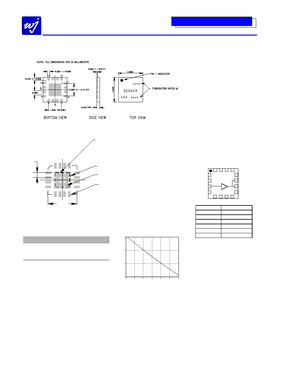
ECP203D (16-pin 4x4mm Package) Mechanical Information
Outline Drawing
Land Pattern
0.65mm
TYP.
TYP.
SOLDERMASK SWELL TO BE 0.5mm
FROM OUTSIDE EDGE OF ALL PADS
GROUND PLANE AREA FOR VIAS
2.23mm X 2.23mm
RECOMMENDED PAD
0.76mm X 0.34mm
DEVICE GROUND PAD
2.0mm X 2.0mm
4.00mm
16L 4.0mm X 4.0mm PACKAGE
0.25mm DIA. THERMAL GROUND VIA HOLE VIAS ARE PLACED
ON A 0.65mm GRID. VIAS ARE TO BE CONNECTED TO TOP,
BOTTOM, AND INTERNAL GROUND PLANES IN ORDER TO
MAXIMIZE HEAT DISSIPATION. FOR .031" THK FR4 MATERIAL,
VIA BARREL PLATING TO BE MIN. 0.0014 THICK. VIAS TO BE
PLUGGED WITH EITHER CONDUCTIVE OR NON-CONDUCTIVE
EPOXY TO PREVENT SOLDER. DRAINS THROUGH VIA IN
REFLOW PROCESS
Thermal Specifications
Parameter
Rating
Operating Case Temperature
-40 to +85
q C
Thermal Resistance, Rth
(1)
17.5
q C / W
Junction Temperature, Tjc
(2)
155
q C
Notes:
1. The thermal resistance is referenced from the junction-
to-case at a case temperature of 85
¢
C. Tjc is a function
of the voltage at pins 10 and 11 and the current applied
to pins 10, 11, and 16 and can be calculated by:
Tjc = Tcase + Rth * Vcc * Icc
2. This corresponds to the typical biasing condition of +5V,
800 mA at an 85
¢
C case temperature. A minimum
MTTF of 1 million hours is achieved for junction
temperatures below 247
¢
C.
Product Marking
The component will be marked with an
" ECP203D" designator with an alphanumeric
lot code on the top surface of the package.
Tape and reel specifications for this part are
located on the website in the " Application
Notes" section.
ESD / MSL Information
ESD Rating: Class 1B
Value:
Passes between 500 and 1000V
Test:
Human Body Model (HBM)
Standard:
JEDEC Standard JESD22-A114
MSL Rating: Level 3 at +235
¢
C convection reflow
Standard:
JEDEC Standard J-STD-020
Functional Diagram
Function
Pin No.
Vref
1
RF Input
3
RF Output
10, 11
Vbias
16
GND
Backside Paddle
N/C or GND
2, 4-9, 12-15
Mounting Config. Notes
1. A heatsink underneath the area of the PCB for the mounted
device is strictly required for proper thermal operation.
Damage to the device can occur without the use of one.
2. Ground / thermal vias are critical for the proper performance
of this device. Vias should use a .35mm (#80 / .0135" )
diameter drill and have a final plated thru diameter of .25
mm (.010" ).
3. Add as much copper as possible to inner and outer layers
near the part to ensure optimal thermal performance.
4. Mounting screws can be added near the part to fasten the
board to a heatsink. Ensure that the ground / thermal via
region contacts the heatsink.
5. Do not put solder mask on the backside of the PC board in
the region where the board contacts the heatsink.
6. RF trace width depends upon the PC board material and
construction.
7. Use 1 oz. Copper minimum.
8
All dimensions are in millimeters (inches). Angles are in
degrees.
1
2
3
4
12
11
10
9
16
15
14
13
5
6
7
8
N/C
RF OUT
RF OUT
N/C
Vref
N/C
RF IN
N/C
V
b
i
a
s
N
/
C
N
/
C
N
/
C
N
/
C
N
/
C
N
/
C
N
/
C
MTTF vs. GND Tab Temperature
100
1000
10000
100000
60
70
80
90
100
110
120
Tab Temperature (∞C)
M
T
T
F
(
m
i
l
l
i
o
n
h
r
s
)