 | –≠–ª–µ–∫—Ç—Ä–æ–Ω–Ω—ã–π –∫–æ–º–ø–æ–Ω–µ–Ω—Ç: FH1 | –°–∫–∞—á–∞—Ç—å:  PDF PDF  ZIP ZIP |
WJ Communications, Inc. ∑ Phone: 1-800-WJ1-4401 ∑ FAX: 408-577-6620 ∑ e-mail: sales@wj.com ∑ Web site: www.wj.com
February 2002
FH1
Product Description
The FH1 is a high dynamic range FET pack-
aged in a low cost surface mount package. The
combination of low noise figure and high out-
put IP3 at the same bias point makes it ideal for
receiver and transmitter applications. The FH1
achieves +42 dBm OIP3 at a mounting tem-
perature of 85∞C with an associated MTBF of
>100 years. The package is a SOT-89. All
devices are 100% RF and DC tested.
The product is targeted for applications where
high linearity is required.
Product Features
∑
50-3000 MHz Bandwidth
∑
+
42 dBm Output IP3
∑
1.2 dB Noise Figure
∑
18 dB Gain
∑
+
21 dBm P1dB
∑
Single or Dual Supply Operation
∑
MTBF >100 Years
∑
SOT-89 SMT Package
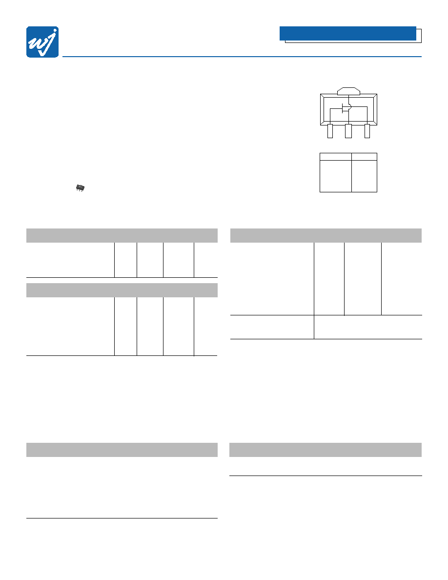
Functional Diagram
4
1
2
3
Function Pin
No.
Gate
1
Source
2
Drain
3
Source
4
High Dynamic Range FET
Advanced Product Information
Ordering Information
Part No.
Description
FH1
High Dynamic Range FET
(Available in tape and reel)
The Communications Edge
TM
Absolute Maximum Ratings
Parameter
Rating
Drain to Source Voltage
+6.0 V
Gate to Source Voltage
-6.0 V
Gate Current
4.5 mA
Operating Case Temperature
-40 to +85∞C
Storage Temperature
-55 to +125∞C
Input RF Power (continuous)
+10 dBm
Operation of this device above any of these parameters may cause permanent damage.
Specifications
DC Electrical Parameter Units
Min.
Typical
Max.
Saturated Drain Current, Idss mA
100
140
170
Transconductance, Gm
mS
120
Pinch Off Voltage, Vp
V
-3.0
-1.5
RF Parameter
Units
Min.
Typical
Max.
Small Signal Gain, Gss
dB
17
18
Max Stable Gain, Gmsg
dB
23
Output IP3
dBm
38
42
Output P1dB
dBm
21
Noise Figure, NF
7
dB 1.2
Notes:
1. DC and RF parameters measured under the following conditions unless otherwise noted.
25∞C with Vds = 5.0 V, Vgs = 0 V, test frequency = 800 MHz, 50
system.
2. OIP3 measured with two tones at an output power of 5 dBm/tone separated by 10 MHz. The
suppression on the largest IM3 product is used to calculate the OIP3 using a 2:1 slope rule.
3. Device needs appropriate match to become unconditionally stable.
4. Degradation of OIP3 occurs at low temperatures. Minimum typical OIP3 at -40∞C is +36 dBm.
5. Idss is measured with Vgs = 0 V.
6. Pinch off voltage is measured when Ids = 0.6 mA.
7. Measured with Vds = 3.3 V, 50% Idss.
Typical Parameters
Parameter
Units
Typical
Frequency MHz
900
1900
S21 dB
19.0
16.0
S11
dB
-10.7
-12.3
S22
dB
-9.7
-17.2
Output IP3
dBm
+44.0
+39.6
Output P1dB
dBm
+21.8
+22.1
Noise Figure
dB
2.7
3.1
Drain Bias Supply
5 V @ 140 mA
Gate Bias
0 V
Typical parameters reflect performance in an application circuit.
Actual Size
WJ Communications, Inc. ∑ Phone: 1-800-WJ1-4401 ∑ FAX: 408-577-6620 ∑ e-mail: sales@wj.com ∑ Web site: www.wj.com
February 2002
FH1
Advanced Product Information
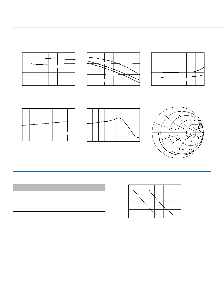
Performance Charts
(Vds = 5.0 V, Ids = 150 mA, T = 22∞C, 50 ohm system)
OIP3 vs. Temperature
OIP3 vs. Power Out
S-Parameters
S11 and S22
NF (dB)
Frequency (GHz)
0
.5
1
1.5
2
3
2.5
NF vs. Frequency
5
0
1
2
3
4
MTBF vs. Temperature
1011
Gain vs. Temperature
Gain (dB)
3
Frequency (GHz)
0
.5
1
1.5
2
2.5
3
23
19
21
17
13
15
11
Gain at +22∞C
Gain at -40∞C
Gain at +85∞C
5V, 100% Idss
5V 100% Idss
3.3V 50% Idss
OIP3 (dB)
Frequency (GHz)
0
.5
1
1.5
2
3
2.5
OIP3 vs. Frequency
50
0
10
20
30
40
5V 100% Idss
3.3V 50% Idss
OIP3 (dBm)
Output Power (dBm)
0
2
4
6
8
12
10
14
16
18
50
45
40
35
30
OIP3 (dBm)
Temperature (∞C)
-40
-20
0
20
40
60
100
80
50
30
35
40
45
5V, 100% Idss
S22
0.05
0.05
2.05
2.05
S11
10
9
10
8
10
7
10
6
10
5
50
75
100
125
150
175
200
Temperature (∞C)
MTBF (hours)
MTBF vs. Temperature
Junction
Ground Tab
Thermal Specifications
Parameter
Rating
Operating Case Temperature
-40 to +125∞C
Thermal Resistance (Maximum)
59∞C/W
Junction Temperature
+155∞C
(Recommended Maximum)
Notes:
1. Thermal Resistance determined at Maximum Tab Temperature and Maximum Power
Dissipation.
2. Recommended Maximum Junction Temperature insures a MTBF of 1 million hours.
WJ Communications, Inc. ∑ Phone: 1-800-WJ1-4401 ∑ FAX: 408-577-6620 ∑ e-mail: sales@wj.com ∑ Web site: www.wj.com
February 2002
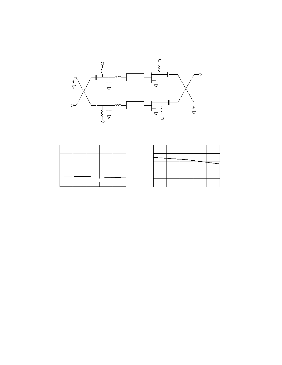
Low Noise Application Circuit
(1880 MHz Balanced Amplifier)
RF OUT
RF IN
47 pF
47 pF
1.0 pF
100 pF
100 pF
1.0 pF
47 nH
68 nH
68 nH
2.55 nH
2.55 nH
47 nH
V6
Vd
Vd = 3.8 V
V6 = -1.0 V
Z = 85 ohm
O = 8∞
Z = 85 ohm
O = 8∞
Noise Figure and OIP3 vs. Frequency
Noise Figure
OIP3
Frequency (MHz)
1830
1850
1870
1890
1910
1930
4
3
2
1
40
35
30
25
OIP3
Noise Figure
Gain
Return Loss
Frequency (MHz)
1830
1850
1870
1890
1910
1930
Gain and Return Loss vs. Frequency
20
10
12
14
16
18
0
-25
-20
-15
-10
-5
Gain
Return Loss
WJ Communications, Inc. ∑ Phone: 1-800-WJ1-4401 ∑ FAX: 408-577-6620 ∑ e-mail: sales@wj.com ∑ Web site: www.wj.com
February 2002
FH1
Advanced Product Information
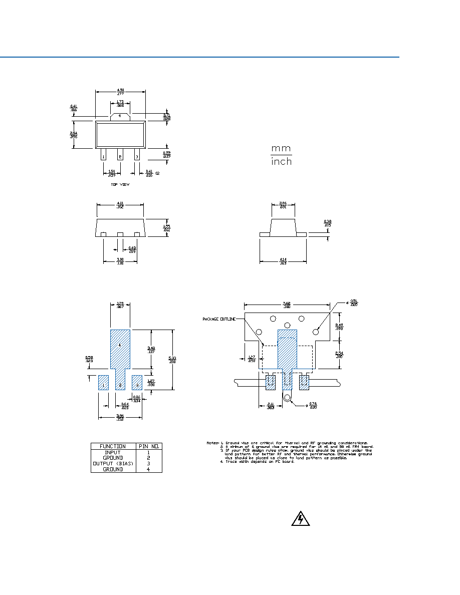
Outline Drawing
Land Pattern
Mounting Configuration
This document contains information on a new product.
Specifications and information are subject to change without notice.
Caution! ESD sensitive device.

WJ Communications, Inc. ∑ Phone: 1-800-WJ1-4401 ∑ FAX: 408-577-6620 ∑ e-mail: sales@wj.com ∑ Web site: www.wj.com
February 2002
FH1
Typical Test Data
S-Parameters (Vds = +5 V, 100% Idss, T = 22∞C, de-embedded into package device in a 50 ohm system)
Freq (GHz) S11 (Mag) S11 (Ang) S21 (dB) S21 (Mag) S21 (Ang) S12 (Mag) S12 (Ang) S22 (Mag) S22 (Ang) K Value
0.05
0.997
-3.940
19.789
9.760
175.000
0.002
97.900
0.502
-6.360
0.0004
0.30
0.993
-22.800
19.370
9.300
162.000
0.015
76.000
0.492
-15.200
0.0570
0.55
0.968
-42.900
19.133
9.050
147.000
0.027
66.100
0.455
-26.300
0.1303
0.80
0.928
-62.100
18.639
8.550
133.000
0.037
54.400
0.424
-36.400
0.2302
1.05
0.905
-79.100
18.116
8.050
121.000
0.046
45.800
0.398
-47.300
0.2490
1.30
0.868
-95.800
17.478
7.480
109.000
0.053
35.500
0.361
-56.700
0.3267
1.55
0.841
-111.000
16.852
6.960
97.500
0.059
27.400
0.329
-66.400
0.3761
1.80
0.815
-126.000
16.191
6.450
86.900
0.063
20.100
0.308
-75.000
0.4231
2.05
0.780
-142.000
15.519
5.970
76.800
0.068
13.400
0.296
-81.500
0.4842
2.30
0.766
-155.000
14.901
5.560
67.300
0.071
6.700
0.268
-89.400
0.5293
2.55
0.754
-168.000
14.253
5.160
58.300
0.073
0.425
0.240
-96.100
0.5844
2.80
0.754
-180.000
13.679
4.830
49.600
0.074
-5.810
0.216
-103.000 0.6190
3.05
0.748
169.000
13.103
4.520
41.200
0.075
-12.300
0.191
-110.000 0.6719
S-Parameters (Vds = +3.3 V, 50% Idss, T = 22∞C, de-embedded into package device in a 50 ohm system)
Freq (GHz) S11 (Mag) S11 (Ang) S21 (dB) S21 (Mag) S21 (Ang) S12 (Mag) S12 (Ang) S22 (Mag) S22 (Ang) K Value
0.05
0.998
-3.580
18.900
8.810
176.000
0.002
105.000
0.387
-3.780
-0.0299
0.30
0.994
-21.200
18.700
8.610
163.000
0.016
78.500
0.392
-16.300
0.0449
0.55
0.973
-39.900
18.547
8.460
149.000
0.030
66.900
0.360
-29.600
0.1249
0.80
0.935
-58.000
18.105
8.040
136.000
0.042
55.800
0.337
-42.100
0.2164
1.05
0.915
-74.200
17.696
7.670
123.000
0.052
46.900
0.317
-55.600
0.2394
1.30
0.880
-90.300
17.122
7.180
112.000
0.061
37.200
0.285
-67.900
0.3035
1.55
0.853
-105.000
16.547
6.720
100.000
0.068
28.700
0.259
-81.000
0.3513
1.80
0.826
-120.000
15.959
6.280
89.900
0.073
20.800
0.250
-93.100
0.3876
2.05
0.788
-136.000
15.402
5.890
79.700
0.080
14.000
0.236
-102.000 0.4513
2.30
0.772
-150.000
14.807
5.500
70.000
0.083
6.160
0.215
-115.000 0.4923
2.55
0.757
-163.000
14.185
5.120
60.800
0.087
-0.455
0.189
-126.000 0.5445
2.80
0.755
-175.000
13.625
4.800
52.000
0.089
-6.810
0.169
-138.000 0.5746
3.05
0.747
174.000
13.064
4.500
43.400
0.090
-13.400
0.150
-152.000 0.6242
Advanced Product Information

WJ Communications, Inc. ∑ Phone: 1-800-WJ1-4401 ∑ FAX: 408-577-6620 ∑ e-mail: sales@wj.com ∑ Web site: www.wj.com
February 2002