
Specifications and information are subject to change without notice.
WJ Communications, Inc
∑
Phone 1-800-WJ1-4401
∑
FAX: 408-577-6621
∑
e-mail: sales@wj.com
∑
Web site: www.wj.com
June
2003
FP1189
Ω-Watt HFET
Product Information
The Communications Edge
TM
Product Features
∑
50 ≠ 4000 MHz
∑
+27 dBm P1dB
∑
+40 dBm Output IP3
∑
High Drain Efficiency
∑
20.5 dB Gain @ 900 MHz
∑
MTTF >100 Years
∑
SOT-89 SMT Package
Applications
∑
Mobile Infrastructure
∑
CATV / DBS
∑
W-LAN / ISM
∑
RFID
∑
Defense / Homeland Security
∑
Fixed Wireless
Product Description
The FP1189 is a high performance Ω-Watt HFET
(Heterostructure FET) in a low-cost SOT-89 surface-
mount package. This device works optimally at a
drain bias of +8 V and 125 mA to achieve +40 dBm
output IP3 performance and an output power of +27
dBm at 1-dB compression, while providing 20.5 dB
gain at 900 MHz.
The device conforms to WJ Communications' long
history of producing high reliability and quality
components. The FP1189 has an associated MTTF
of greater than 100 years at a mounting temperature
of 85
∞
C. All devices are 100% RF & DC tested.
The product is targeted for use as driver amplifiers
for wireless infrastructure where high performance
and high efficiency are required.
Functional Diagram
Function Pin
No.
Input / Gate
1
Output / Drain
3
Ground 2,
4
Specifications
DC Parameter
Units Min Typ Max
Saturated Drain Current, I
dss
(1) mA 220 290 360
Transconductance, G
m
mS
155
Pinch Off Voltage, V
p
(2)
V
-2.1
Thermal Resistance
∞
C / W
68
Junction Temperature (3)
∞
C
160
RF Parameter (4)
Units Min Typ Max
Frequency Range
MHz
50
900
4000
Small Signal Gain
dB
20.5
SS Gain (50
, unmatched)
dB
17
21
Maximum Stable Gain
dB
24
Output P1dB
dBm
+27.4
Output IP3 (5)
dBm
+40
Noise Figure
dB
2.7
1. I
dss
is measured with V
gs
= 0 V, V
ds
= 3 V.
2. Pinch-off voltage is measured when I
ds
= 1.2 mA.
3. The junction temperature ensures a minimum MTTF rating of 1 million hours of usage.
4. Test conditions unless otherwise noted: T = 25∫C, V
DS
= 8 V, I
DQ
= 125 mA, frequency = 900 MHz in
a tuned application circuit with Z
L
= Z
LOPT
, Z
S
= Z
SOPT
(optimized for output power).
5. 3OIP measured with two tones at an output power of +12 dBm/tone separated by 1 MHz. The
suppression on the largest IM3 product is used to calculate the 3OIP using a 2:1 rule.
Typical Performance
Parameter (6) Units
Typical
Frequency MHz
915
1960
2140
S21
dB 20.6 15.7 14.7
S11
dB -13 -26 -24
S22
dB -6.0 -9.6 -9.0
Output
P1dB
dBm +27.4 +27.2 +27.2
Output
IP3
dBm +39.9 +40.4 +39.7
Noise
Figure
dB 2.7 3.7 4.3
Channel Power (7)
@ -45 dBc ACPR
dBm +21 +20.8
+18.4
Drain Voltage
V
+8
Drain Current
mA
125
6. Typical parameters represent performance in an application circuit.
7. An IS-95 signal is used for 915 / 1960 MHz. A 3GPP W-CDMA signal is used for 2140 MHz.
Absolute Maximum Rating
Ordering Information
Parameter
Rating
Part No.
Description
Operating Case Temperature
-40 to +85
∞
C
FP1189
Ω -Watt HFET
Storage Temperature
-55 to +125
∞
C
FP1189-PCB900S
870 ≠ 960 MHz Application Circuit
DC Power
2.0 W
FP1189-PCB1900S
1930 ≠ 1990 MHz Application Circuit
RF Input Power (continuous)
6 dB above Input P1dB
FP1189-PCB2140S
2110 ≠ 2170 MHz Application Circuit
Drain to Gate Voltage, V
dg
+14
V
Junction Temperature
+220
∞
C
Operation of this device above any of these parameters may cause permanent damage.
RF IN
GND
RF OUT
GND
1
2
3
4
Specifications and information are subject to change without notice.
WJ Communications, Inc
∑
Phone 1-800-WJ1-4401
∑
FAX: 408-577-6621
∑
e-mail: sales@wj.com
∑
Web site: www.wj.com
June
2003
FP1189
Ω-Watt HFET
Product Information
The Communications Edge
TM
Typical Device Data
S-Parameters (V
DS
= +8 V, I
DS
= 125 mA, T = 25
∞
C, calibrated to device leads)
0
1
2
3
4
5
6
Frequency (GHz)
S21, Maximum Stable Gain vs. Frequency
0
5
10
15
20
25
30
S
2
1
,
MS
G
(d
B
)
DB(|S[2,1]|)
DB(MSG)
0
1.
0
1.
0
-1
.0
10
.0
10.0
-10
.0
5.
0
5.
0
-5
.0
2.
0
2.
0
-2
.0
3.
0
3.
0
-3
.0
4.
0
4.
0
-4
.0
0.
2
0 .
2
-0
.2
0.
4
0 .
4
-0
.4
0.
6
0 .
6
-0
.
6
0.
8
0.
8
-0
.8
S11
Swp Max
6GHz
Swp Min
0.05GHz
0
1.
0
1.
0
-1
.0
10
.0
10.0
- 1
0.
0
5.
0
5.
0
-5
.0
2.
0
2.
0
- 2
.
0
3.
0
3.
0
-3
.0
4.
0
4.
0
-4
.0
0.
2
0.
2
-0
.2
0.
4
0.
4
-0
.4
0.
6
0.
6
-0
.6
0.
8
0.
8
-0
.8
S22
Swp Max
6GHz
Swp Min
0.05GHz
Note:
Measurements were made on the packaged device in a test fixture with 50 ohm input and output lines.
The S-parameters shown are the de-embedded data down to the device leads and represents typical performance of the device.
Freq (MHz)
S11 (mag)
S11 (ang)
S21 (mag)
S21 (ang)
S12 (mag)
S12 (ang)
S22 (mag)
S22 (ang)
50 1.000 -4.52 10.313
176.55 0.002 87.44 0.544 -3.02
250 0.988 -21.51 10.120 163.88 0.010 76.64 0.535 -13.77
500 0.959 -42.21 9.681 148.45 0.020 64.73 0.520 -27.13
750 0.933 -61.23 9.005 134.71 0.028 53.45 0.495 -39.31
1000 0.895 -78.75 8.270 122.08 0.035 44.25 0.469 -50.54
1250 0.860 -95.09 7.561 109.58 0.040 34.30 0.447 -60.96
1500 0.848 -109.61 7.028 99.15 0.044 26.69 0.428 -70.64
1750 0.821 -122.91 6.408 88.96 0.046 19.57 0.407 -79.82
2000 0.807 -135.32 5.950 79.64 0.048 13.93 0.400 -88.93
2250 0.796 -147.01 5.474 70.37 0.049 7.21 0.386 -97.59
2500 0.785 -157.00 5.087 62.43 0.050 2.99 0.374 -105.24
2750 0.780 -166.26 4.732 53.97 0.050 -1.58 0.376 -113.47
3000 0.775 -175.87 4.415 45.54 0.049 -6.79 0.369 -121.84
3250 0.766 175.78 4.082 38.18 0.049 -9.36 0.368 -129.77
3500 0.770 167.34 3.843 30.76 0.048 -12.48 0.372 -137.25
3750 0.771 159.87 3.602 23.91 0.050 -14.97 0.369 -144.61
4000 0.771 152.07 3.408 16.74 0.050 -17.53 0.374 -152.17
4250 0.771 145.63 3.241 9.15 0.048 -19.53 0.382 -161.00
4500 0.772 138.97 3.053 2.49 0.048 -21.27 0.387 -168.31
4750 0.770 132.07 2.876 -4.50 0.050 -23.00 0.396 -175.08
5000 0.780 126.56 2.743 -10.47 0.048 -25.08 0.408 177.65
5250 0.794 120.21 2.622 -17.28 0.049 -26.64 0.412 170.89
5500 0.795 114.22 2.507 -24.43 0.051 -30.44 0.423 162.41
5750 0.794 108.27 2.346 -31.21 0.052 -30.16 0.442 154.66
6000 0.798 102.86 2.237 -36.95 0.052 -31.18 0.446 147.41
Device S-parameters are available for download off of the website at: http://www.wj.com
1
2
3
4
5
6
1
2
3
4
5
6
Specifications and information are subject to change without notice.
WJ Communications, Inc
∑
Phone 1-800-WJ1-4401
∑
FAX: 408-577-6621
∑
e-mail: sales@wj.com
∑
Web site: www.wj.com
June
2003
FP1189
Ω-Watt HFET
Product Information
The Communications Edge
TM
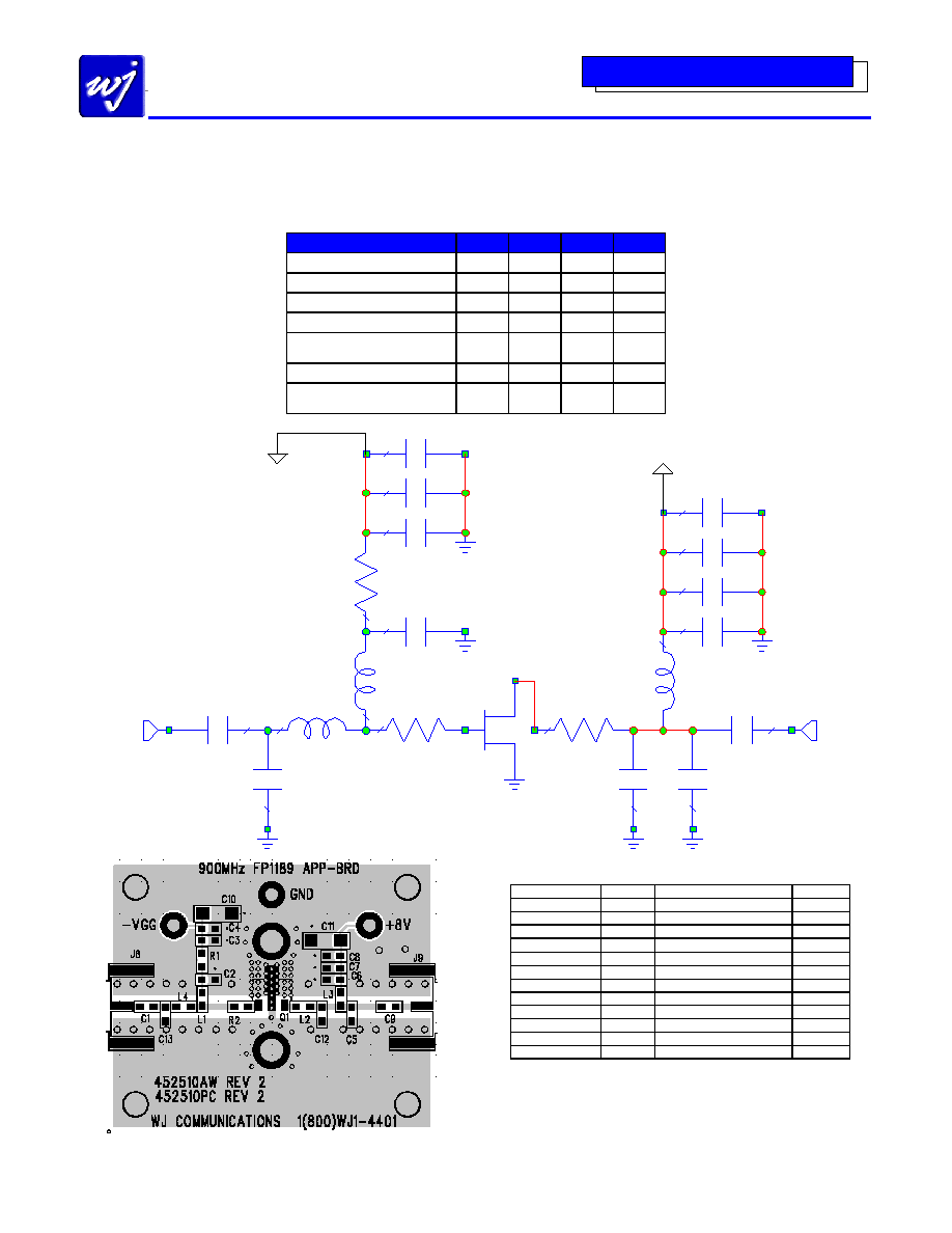
Application Circuit: 870 ≠ 960 MHz (FP1189-PCB900S)
The application circuit is matched for output power.
Typical RF Performance
Drain Bias = +8 V, I
ds
= 125 mA, 25
∞
∞
∞
∞
C
Frequency
MHz
870
915
960
S21 ≠ Gain
dB
20.9
20.6
19.8
S11 ≠ Input Return Loss
dB
-10
-13
-10
S22 ≠ Output Return Loss
dB
-5.2
-6.0
-7.6
Output P1dB
dBm
+27.5
+27.4
+27.5
Output IP3
(+12 dBm / tone, 1 MHz spacing)
dBm +39.9
Noise Figure
dB
2.7
2.7
2.6
IS-95 Channel Power
@ -45 dBc ACPR
dBm +21
RES
R=
ID=
10 Ohm
R2
IND
L=
ID=
12 nH
L4
CAP
C=
ID=
3.9 pF
C13
IND
L=
ID=
47 nH
L1
RES
R=
ID=
20 Ohm
R1
CAP
C=
ID=
68 pF
C1
CAP
C=
ID=
18 pF
C2
CAP
C=
ID=
6 8 p F
C3
CAP
C=
ID=
100 0 p F
C4
CAP
C=
ID=
DNP pF
C10
RES
R=
ID=
0 Ohm
L2
CAP
C=
ID=
DNP pF
C12
IND
L=
ID=
47 nH
L3
CAP
C=
ID=
18 pF
C6
CAP
C=
ID=
68 pF
C7
CAP
C=
ID=
1000 pF
C8
CAP
C=
ID=
1e5 pF
C11
CAP
C=
ID=
DNP pF
C5
CAP
C=
ID=
68 pF
C9
1
2
SUBCKT
NET=
ID=
"FP1189"
Q1
PORT
Z=
P=
50 Ohm
1
PORT
Z=
P=
50 Ohm
2
-Vgg
Vds = 8 V @ 125 mA
14 mil GETEK
TM
ML200DSS (
r
= 4.2)
The main microstrip line has a line impedance of 50 .
Bill of Materials
Ref. Desig.
Value
Part style
Size
C1, C3, C7, C9
68 pF
Chip capacitor
0603
C2, C6
18 pF
Chip capacitor
0603
C4, C8
1000 pF
Chip capacitor
0603
C11
0.1
µ
F
Chip capacitor
1206
C13
3.9 pF
Chip capacitor
0603
L1, L3
47 nH
Multilayer chip inductor
0603
L2 0
Chip
resistor
0603
L4
12 nH
Multilayer chip inductor
0603
R1 10
Chip
resistor
0603
R2 20
Chip
resistor
0603
Q1
FP1189
WJ 0.5W HFET
SOT-89
C5, C12, C10
Do Not Place
Specifications and information are subject to change without notice.
WJ Communications, Inc
∑
Phone 1-800-WJ1-4401
∑
FAX: 408-577-6621
∑
e-mail: sales@wj.com
∑
Web site: www.wj.com
June
2003
FP1189
Ω-Watt HFET
Product Information
The Communications Edge
TM
FP1189-PCB900S Application Circuit Performance Plots
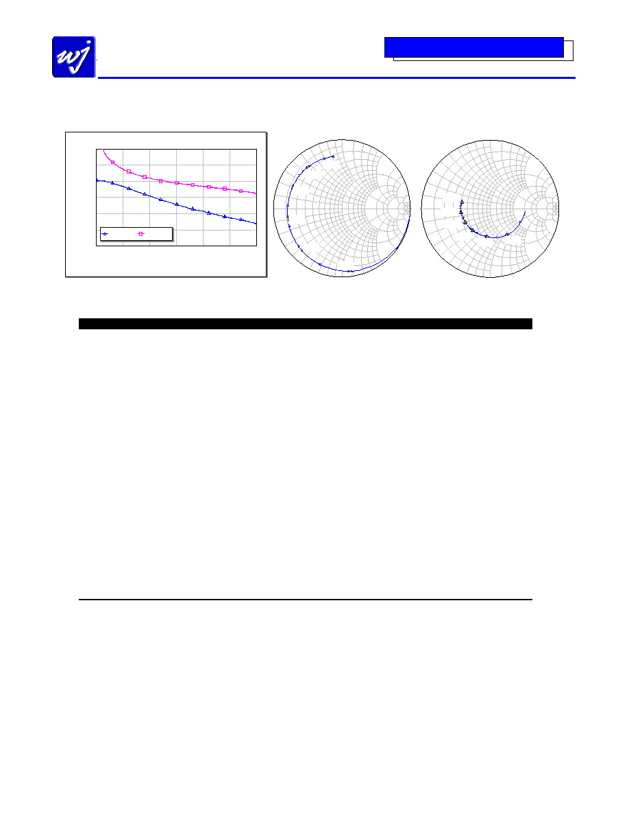
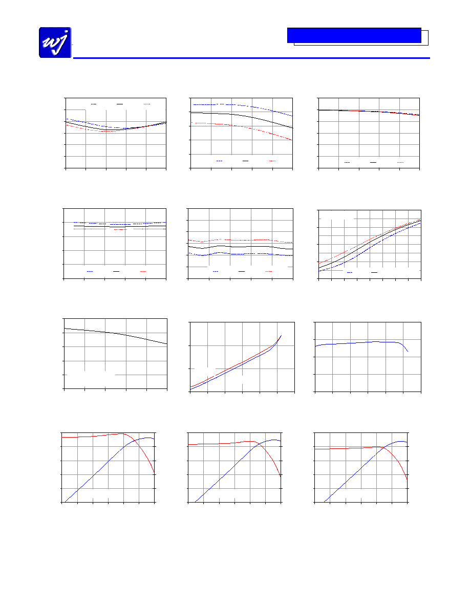
S11 vs. Frequency
-30
-25
-20
-15
-10
-5
0
860
880
900
920
940
960
Frequency (MHz)
S11 (dB)
-40c
+25c
+85c
S21 vs. Frequency
17
18
19
20
21
22
860
880
900
920
940
960
Frequency (MHz)
S21 (dB)
-40c
+25c
+85c
S22 vs. Frequency
-30
-25
-20
-15
-10
-5
0
860
880
900
920
940
960
Frequency (MHz)
S22 (dB)
-40c
+25c
+85c
P1dB vs. Frequency
20
22
24
26
28
30
860
880
900
920
940
960
Frequency (MHz)
P1dB (dBm)
-40c
+25c
+85c
Noise Figure vs. Frequency
0
1
2
3
4
5
6
860
880
900
920
940
960
Frequency (MHz)
NF (dB)
-40c
+25c
+85c
ACPR vs. Channel Power
IS-95, 9 Ch. Forward, ±885 kHz offset, 30 kHz Meas BW
-70
-60
-50
-40
-30
16
17
18
19
20
21
22
23
24
Output Channel Power (dBm)
ACPR (dBc)
-40 C
+25 C
+85 C
freq = 915 MHz
OIP3 vs. Temperature
32
34
36
38
40
42
-40
-15
10
35
60
85
Temperature (∞C)
OIP3 (dBm)
freq = 915, 916 MHz
+12 dBm / tone
IMD products vs. Output Power
fundamental frequency = 915 MHz, 916 MHz; Temp = +25∞ C
-80
-60
-40
-20
0
4
8
12
16
20
24
Output Power (dBm)
IMD products (dBm)
IMD_Low
IMD_High
OIP3 vs. Output Power
fundamental frequency = 915 MHz, 916 MHz; Temp = +25∞ C
25
30
35
40
45
0
4
8
12
16
20
24
Output Power (dBm)
OIP3 (dBm)
Output Power / Gain vs. Input Power
frequency = 915 MHz, Temp = -40∞ C
12
14
16
18
20
22
-12
-8
-4
0
4
8
12
Input Power (dBm)
Gain (dB)
10
14
18
22
26
30
Out
p
ut Power
(
dBm
)
Output Power
Gain
Output Power / Gain vs. Input Power
frequency = 915 MHz, Temp = +25∞ C
12
14
16
18
20
22
-12
-8
-4
0
4
8
12
Input Power (dBm)
Gain (dB)
10
14
18
22
26
30
Out
p
ut Power
(
dBm
)
Output Power
Gain
Output Power / Gain vs. Input Power
frequency = 915 MHz, Temp = +85∞ C
12
14
16
18
20
22
-12
-8
-4
0
4
8
12
Input Power (dBm)
Gain (dB)
10
14
18
22
26
30
Out
p
ut Power
(
dBm
)
Output Power
Gain

Specifications and information are subject to change without notice.
WJ Communications, Inc
∑
Phone 1-800-WJ1-4401
∑
FAX: 408-577-6621
∑
e-mail: sales@wj.com
∑
Web site: www.wj.com
June
2003
FP1189
Ω-Watt HFET
Product Information
The Communications Edge
TM
Application Circuit: 1930 ≠ 1990 MHz (FP1189-PCB1900S)
The application circuit is matched for output power.
Typical RF Performance
Drain Bias = +8 V, I
ds
= 125 mA, 25
∞
∞
∞
∞
C
Frequency
MHz
1930
1960
1990
S21 ≠ Gain
dB
15.8
15.7
15.5
S11 ≠ Input Return Loss
dB
-26
-26
-24
S22 ≠ Output Return Loss
dB
-9.2
-9.6
-9.0
Output P1dB
dBm
+27.4
+27.2
+27.4
Output IP3
(+12 dBm / tone, 1 MHz spacing)
dBm +40.4
Noise Figure
dB
3.7
IS-95 Channel Power
@ -45 dBc ACPR
dBm +20.8
RES
R=
ID=
10 Ohm
R2
CAP
C=
ID=
DNP pF
C13
IND
L=
ID=
22 nH
L1
RES
R=
ID=
100 Ohm
R1
CAP
C=
ID=
33 pF
C1
CAP
C=
ID=
DNP pF
C2
IND
L=
ID=
22 nH
L3
CAP
C=
ID=
33 pF
C6
CAP
C=
ID=
DNP pF
C7
CAP
C=
ID=
DNP pF
C8
CAP
C=
ID=
DNP pF
C12
CAP
C=
ID=
0.5 pF
C5
CAP
C=
ID=
33 pF
C9
CAP
C=
ID=
1.8 pF
C15
CAP
C=
ID=
DNP pF
C13
IND
L=
ID=
2.7 nH
L2
CAP
C=
ID=
1e5 pF
C11
CAP
C=
ID=
DNP pF
C3
CAP
C=
ID=
33 pF
C4
CAP
C=
ID=
DNP pF
C10
1
2
SUBCKT
NET=
ID=
"FP1189"
Q1
PORT
Z=
P=
50 Ohm
1
PORT
Z=
P=
50 Ohm
2
-Vgg
Vds = 8 V @ 125 mA
14 mil GETEKTM ML200DSS (r = 4.2)
The main microstrip line has a line impedance of 50 .
Bill of Materials
Ref. Desig.
Value
Part style
Size
C1, C4, C6, C9
33 pF
Chip capacitor
0603
C5
0.5 pF
Chip capacitor
0603
C11
0.1
µ
F
Chip capacitor
1206
C15
1.8 pF
Chip capacitor
0603
L1, L3
22 nH
Multilayer chip inductor
0603
L2
2.7 nH
Multilayer chip inductor
0603
R1 100
Chip
resistor
0603
R2 10
Chip
resistor
0603
Q1
FP1189
WJ 0.5W HFET
SOT-89
C2, C3, C7, C8,
C10, C12, C13, C14
Do Not Place