 | –≠–ª–µ–∫—Ç—Ä–æ–Ω–Ω—ã–π –∫–æ–º–ø–æ–Ω–µ–Ω—Ç: FP2189 | –°–∫–∞—á–∞—Ç—å:  PDF PDF  ZIP ZIP |
This document contains information on a new product.
Specifications and information are subject to change without notice
WJ Communications, Inc
∑ Phone 1-800-WJ1-4401 ∑ FAX: 408-577-6620 ∑ e-mail: sales@wj.com ∑ Web site: www.wj.com
May 2002
The Communications Edge
TM
Preliminary Product Information
FP2189
1 Watt HFET
Product Features
∑
50 ≠ 4000 MHz
∑
Up to +31 dBm P1dB
∑
Up to +45 dBm Output IP3
∑
High Drain Efficiency
∑
19 dB Gain @ 900 MHz
∑
MTBF >100 Years
∑
SOT-89 SMT Package
Product Description
The FP2189 is a high performance 1-Watt HFET
(Heterostructure FET) in a low-cost SOT-89 surface-
mount package. This device works optimally at a drain
bias of +8 V and 250 mA to achieve +4
5 dBm output
IP3 performance and an output power of +31 dBm at
1-dB compression.
The device conforms to WJ Communications' long
history of producing high reliability and quality
components. The FP2189 has an associated MTBF of
greater than 100 years at a mounting temperature of
85
∞C. All devices are 100% RF & DC tested.
The product is targeted for use as driver amplifiers for
wireless infrastructure where high performance and high
efficiency are required.
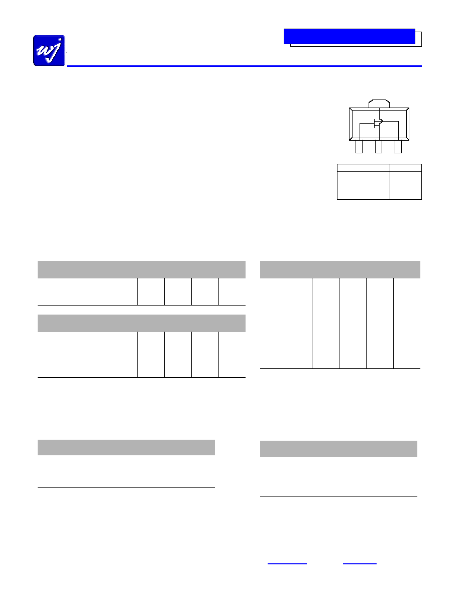
Functional Diagram
1
3
2
4
Function Pin
No.
Input 1
Ground 2
Output/Bias 3
Ground 4
Specifications
DC Electrical Parameter Units Min
Typ
Max
Saturated Drain Current
1
, I
dss
mA 500
Transconductance, G
m
mS
350
Pinch Off Voltage
2
, V
p
V
-2.0
Parameters
3
Units Min
Typ
Max
Frequency Range
MHz
50
4000
Small Signal Gain, Gss
dB
15
Output P1dB
dBm
+31
Output IP3
4
dBm
+45
Thermal Resistance
∞C/W
30
1. I
dss
is measured with V
gs
= 0 V, V
ds
= 3 V.
2. Pinch-off voltage is measured when I
ds
= 0.4 mA.
3. Test conditions unless otherwise noted: T = 25∫C, V
DS
= 8 V, I
DQ
= 250 mA, frequency = 900 MHz
in an application circuit with Z
L
= Z
LOPT
, Z
S
= Z
SOPT
.
4. 3OIP measured with two tones at an output power of +15 dBm/tone separated by 1 MHz. The
suppression on the largest IM3 product is used to calculate the 3OIP using a 2:1 rule.
Absolute Maximum Ratings
Parameters
Rating
Operating Case Temperature
-40 to +85
∞C
Storage Temperature
-40 to +125
∞C
Maximum DC Power
4.0 W
RF Input Power (continuous)
+20 dBm
Operation of this device above any of there parameters may cause permanent damage
Typical Parameters
5
Parameter
Units
Typical
Frequency
MHz 915 1960 2140
S21 dB
19.1 15.2 13.8
S11 dB
-17 -16 -23
S22 dB
-10 -8 -9
Output P1dB
dBm
+30.3 +30.8 +31.4
Output IP3
dBm
+44.3 +44.2 +45.5
Noise Figure
dB
4.2 3.5 4.5
V
dd
V
+8 +8 +8
I
dq
6
mA
250 250 250
I
dd
at P1dB
mA
260 330 320
5.
Typical parameters represent performance in an application circuit.
6. I
dq
is the quiescent drain current at small signal output levels. The
current may increase as the output power is increased near its
compression point.
Ordering Information
Part No.
Description
FP2189
1-Watt HFET
(Available in Tape & Reel)
FP2189-PCB900S
900 MHz Application Circuit
FP2189-PCB1900S 1900 MHz Application Circuit
FP2189-PCB2140S 2140 MHz Application Circuit

This document contains information on a new product.
Specifications and information are subject to change without notice
WJ Communications, Inc
∑ Phone 1-800-WJ1-4401 ∑ FAX: 408-577-6620 ∑ e-mail: sales@wj.com ∑ Web site: www.wj.com
May 2002
The Communications Edge
TM
Preliminary Product Information
FP2189
1 Watt HFET
Typical Performance Data
S-Parameters (V
ds
= 8 V, I
ds
= 250 mA, 25∞C, Unmatched 50 ohm system)
Note:
Measurements were made on the packaged device in a test fixture with 50 ohm input and output lines. The S-parameters
that are shown are the de-embedded data down to the device leads and represents typical performance of the device.
S
22
vs Frequency
1 GHz
S
11
vs Frequency
1 GHz
2 GHz
3 GHz
4 GHz
5 GHz
6 GHz
2 GHz
3 GHz
4 GHz
5 GHz
6 GHz
Gain, Maximum Stable Gain vs Frequency
S21
G
msg

This document contains information on a new product.
Specifications and information are subject to change without notice
WJ Communications, Inc
∑ Phone 1-800-WJ1-4401 ∑ FAX: 408-577-6620 ∑ e-mail: sales@wj.com ∑ Web site: www.wj.com
May 2002
The Communications Edge
TM
Preliminary Product Information
FP2189
1 Watt HFET
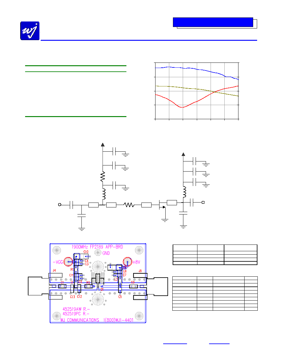
Application Circuit: 870 ≠ 960 MHz
Typical Specifications
Frequency
870 915 960
S21 - Gain
19.1 19.1 19.1
S11 - Input R.L.
-12 -17 -25
S22 - Output R.L.
-9 -10 -12
Output P1dB
+30.4 +30.3 +30.2
Output IP3
+44.4 +44.3 +44.3
Noise Figure
4.2 4.2 4.2
V
dd
+ 8 V
I
dq
1
250 mA
1
I
dq
is the quiescent current at small signal output levels. The current typically
increases up to 260 mA at the 1-dB compression point.
S-Parameters vs Frequency
-30
-20
-10
0
10
800
850
900
950
1000
Frequency (MHz)
S11, S22, S12 (dB)
12
14
16
18
20
S21 (dB)
S21
S11
S22
V
dd
+ 8 V @ 250 mA
RF OUT
RF IN
C1
100 pF
-V
gg
Z1
FP2189
Sot-89
PIN 1
PIN 3
PIN 2,4
Z2
Z3
Z4
Z5
Z6
Z7
C14
4.7 pF
L4
5.6 nH
L1
18 nH
R1
100
C3
100 pF
C4
1000 pF
R2
10
L2
5.6 nH
C5
3 pF
C9
100 pF
L3
82 nH
C7
100 pF
C8
1000 pF
C12
0.1 µF
Ref. Designator
Length on .014"
GETEK
TM
(mil)
Electrical length @
900 MHz (deg)
Z1 30
1.45
Z2 30
1.45
Z3 135
6.5
Z4 50
2.4
Z5 50
2.4
Z6 42
2.0
Z7 65
3.1
The lengths are measured from the component edge-to-edge.
All microstrip lines have a line impedance of 50 .
Ref. Designator
Value
Part style
Size
C1, C3, C7, C9
100 pF
5% 50V, NPO/COG
0603
C4, C8
1000 pF
5%, 50V, NPO/COG
0603
C5 3
pF
AVX 06031J3R0BAWTR
0603
C11 0.1
µF
10%, 50V, X7R
1206
C14 4.7
pF
AVX 06035J4R7APWTR
0603
R1 100
1/16 W, 5%
0603
R2 10
1/16 W, 5%
0603
L1 18
nH
TOKO LL1608-FH18NJ
0603
L2, L4
5.6 nH
TOKO LL1608-FH5N6S
0603
L3 82
nH
TOKO LL1608-FH82NJ
0603
All other parts are No Loads.
Total unique parts count: 10
14 mil GETEK
TM
ML200DSS (
r
= 4.2)
The layout of this circuit can be downloaded from the website.
This document contains information on a new product.
Specifications and information are subject to change without notice
WJ Communications, Inc
∑ Phone 1-800-WJ1-4401 ∑ FAX: 408-577-6620 ∑ e-mail: sales@wj.com ∑ Web site: www.wj.com
May 2002
The Communications Edge
TM
Preliminary Product Information
FP2189
1 Watt HFET
Application Circuit: 1930 ≠ 1990 MHz
Typical Specifications
Frequency
1930 1960 1990
S21 - Gain
15.3 15.2 15.0
S11 - Input R.L.
-14 -16 -19
S22 - Output R.L.
-8 -8 -9
Output P1dB
+30.8 +30.8 +30.7
Output IP3
+44 +44.2 +44.3
Noise Figure
3.6 3.5 3.5
V
dd
+ 8 V
I
dq
1
250 mA
1
I
dq
is the quiescent current at small signal output levels. The current typically
increases up to 330 mA at the 1-dB compression point.
S-Parameters vs Frequency
-30
-20
-10
0
10
1800
1850
1900
1950
2000
2050
2100
Frequency (MHz)
S11, S22, S12 (dB)
8
10
12
14
16
S21 (dB)
S21
S11
S22
Ref. Designator
Length on .014"
GETEK
TM
(mil)
Electrical length @
1900 MHz (deg)
Z1 30
3.1
Z2 145
14.8
Z3 50
5.1
Z4 255
26.1
The lengths are measured from the component edge-to-edge.
All microstrip lines have a line impedance of 50 .
Ref. Designator
Value
Part style
Size
C1, C3, C6, C9
33 pF
5% 50V, NPO/COG
0603
C2, C13
2.4 pF
AVX 06035J2R4AAWTR
0603
C4, C7
1000 pF
5% 50V, NPO/COG
0603
C5 1.5
pF
AVX 06035J1R5AAWTR
0603
C8 0.1
µF
10%, 50V, X7R
1206
R1 20
1/16 W, 5%
0603
R2 5.1
1/16 W, 5%
0603
L1 10
nH
TOKO LL1608-FH10NJ
0603
L2 22
nH
TOKO LL1608-FH22NJ
0603
All other parts are No Loads.
Total unique parts count: 9
14 mil GETEK
TM
ML200DSS (
r
= 4.2)
The layout of this circuit can be downloaded from the website.
V
dd
+ 8 V @ 250 mA
RF OUT
RF IN
C1
33 pF
-V
gg
Z1
FP2189
Sot-89
PIN 1
PIN 3
PIN 2,4
Z2
Z3
Z4
C13
2.4 pF
L1
10 nH
R1
20
C3
33 pF
C4
1000 pF
R2
5.1
C5
1.5 pF
C9
33 pF
L2
22 nH
C7
1000 pF
C6
33 pF
C8
0.1 µF
C2
2.4 pF
This document contains information on a new product.
Specifications and information are subject to change without notice
WJ Communications, Inc
∑ Phone 1-800-WJ1-4401 ∑ FAX: 408-577-6620 ∑ e-mail: sales@wj.com ∑ Web site: www.wj.com
May 2002
The Communications Edge
TM
Preliminary Product Information
FP2189
1 Watt HFET
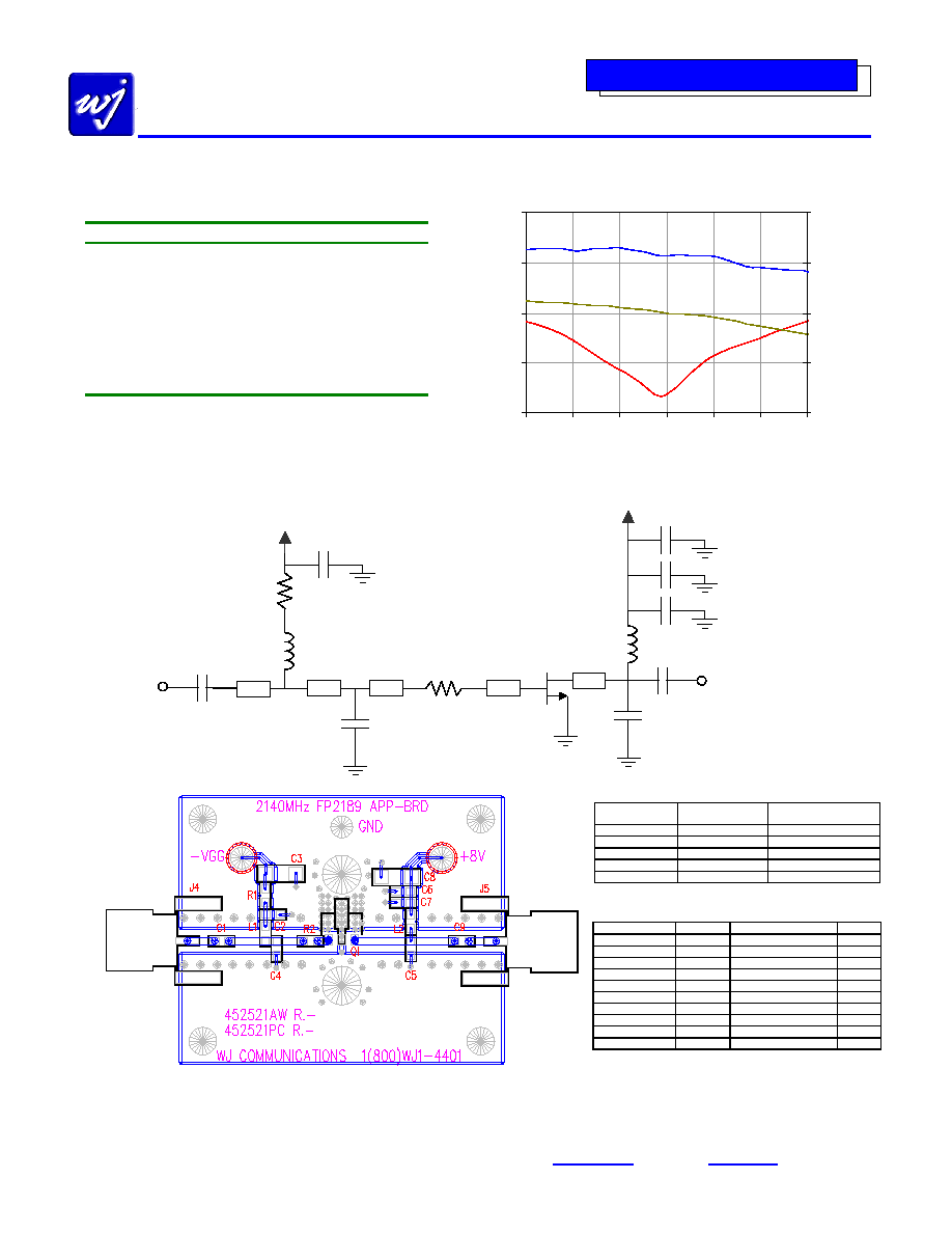
Application Circuit: 2110 ≠ 2170 MHz
Typical Specifications
Frequency
2110 2140 2170
S21 - Gain
13.9 13.8 13.7
S11 - Input R.L.
-27 -23 -20
S22 - Output R.L.
-8 -9 -10
Output P1dB
+31.4 +31.4 +31.4
Output IP3
+44.5 +45.5 +43.2
Noise Figure
4.5 4.5 4.5
V
dd
+ 8 V
I
dq
1
250 mA
1
I
dq
is the quiescent current at small signal output levels. The current typically
increases up to 320 mA at the 1-dB compression point.
S-Parameters vs Frequency
-30
-20
-10
0
10
2000
2050
2100
2150
2200
2250
2300
Frequency (MHz)
S11, S22, S12 (dB)
8
10
12
14
16
S21 (dB)
S21
S11
S22
14 mil GETEK
TM
ML200DSS (
r
= 4.2)
The layout of this circuit can be downloaded from the website.
Ref. Designator
Length on .014"
GETEK
TM
(mil)
Electrical length @
2140 MHz (deg)
Z1 150
17.3
Z2 15
1.7
Z3 100
11.5
Z4 50
5.8
Z5 225
25.9
The lengths are measured from the component edge-to-edge.
All microstrip lines have a line impedance of 50 .
Ref. Designator
Value
Part style
Size
C1 1.8
pF
AVX 06035J1R8AAWTR
0603
C3, C7, C9
22 pF
5% 50V, NPO/COG
0603
C4 1.5
pF
AVX 06035J1R5AAWTR
0603
C5 1.2
pF
AVX 06035J1R2AAWTR
0603
C6 1000
pF
5% 50V, NPO/COG
0603
C8 0.1
µF
10%, 50V, X7R
1206
R1 10
1/16 W, 5%
0603
R2 6.2
1/16 W, 5%
0603
L1 18
nH
TOKO LL1608-FH18NJ
0603
L2 5.6
nH
TOKO LL1608-FH5N6S
0603
All other parts are No Loads.
Total unique parts count: 10
C3 is of size 0805 on the app board so that it would fit in the 1206 pad.
V
dd
+ 8 V @ 250 mA
RF OUT
RF IN
C1
1.8 pF
-V
gg
Z1
FP2189
Sot-89
PIN 1 PIN 3
PIN 2,4
Z2
Z4
Z5
C4
1.5 pF
L1
5.6 nH
R1
10
C4
22 pF
R2
5.1
C5
1.2 pF
C9
22 pF
L2
18 nH
C7
22 pF
C6
1000 pF
C8
0.1 µF
Z3