 | –≠–ª–µ–∫—Ç—Ä–æ–Ω–Ω—ã–π –∫–æ–º–ø–æ–Ω–µ–Ω—Ç: FP31QF-F | –°–∫–∞—á–∞—Ç—å:  PDF PDF  ZIP ZIP |
Specifications and information are subject to change without notice
WJ Communications, Inc
∑
Phone 1-800-WJ1-4401
∑
FAX: 408-577-6621
∑
e-mail: sales@wj.com
∑
Web site: www.wj.com
November
2004
FP31QF
2-Watt HFET
Product Information
The Communications Edge
TM
Product Features
∑
50 ≠ 4000 MHz
∑
18 dB Gain @ 900 MHz
∑
+34 dBm P1dB
∑
+46 dBm Output IP3
∑
High Drain Efficiency
∑
Pb-free 6mm 28-pin QFN package
∑
MTTF > 100 years
Applications
∑
Mobile Infrastructure
∑
CATV / DBS
∑
W-LAN / ISM
∑
RFID
∑
Defense / Homeland Security
∑
Fixed Wireless
Product Description
The FP31QF is a high performance 2-Watt HFET
(Heterostructure FET) in a low-cost lead-free 28-pin 6x6
mm QFN (Quad Flatpack, No-Lead) surface-mount
package. This device works optimally at a drain bias of
+9 V and 450 mA to achieve +46 dBm output IP3
performance and an output power of +34 dBm at 1-dB
compression.
The device conforms to WJ Communications' long
history of producing high reliability and quality
components. The FP31QF has an associated MTTF of a
minimum of 100 years at a mounting temperature of
85
∞C. All devices are 100% RF & DC tested.
The product is targeted for use as driver amplifiers for
wireless infrastructure where high performance and high
efficiency are required.
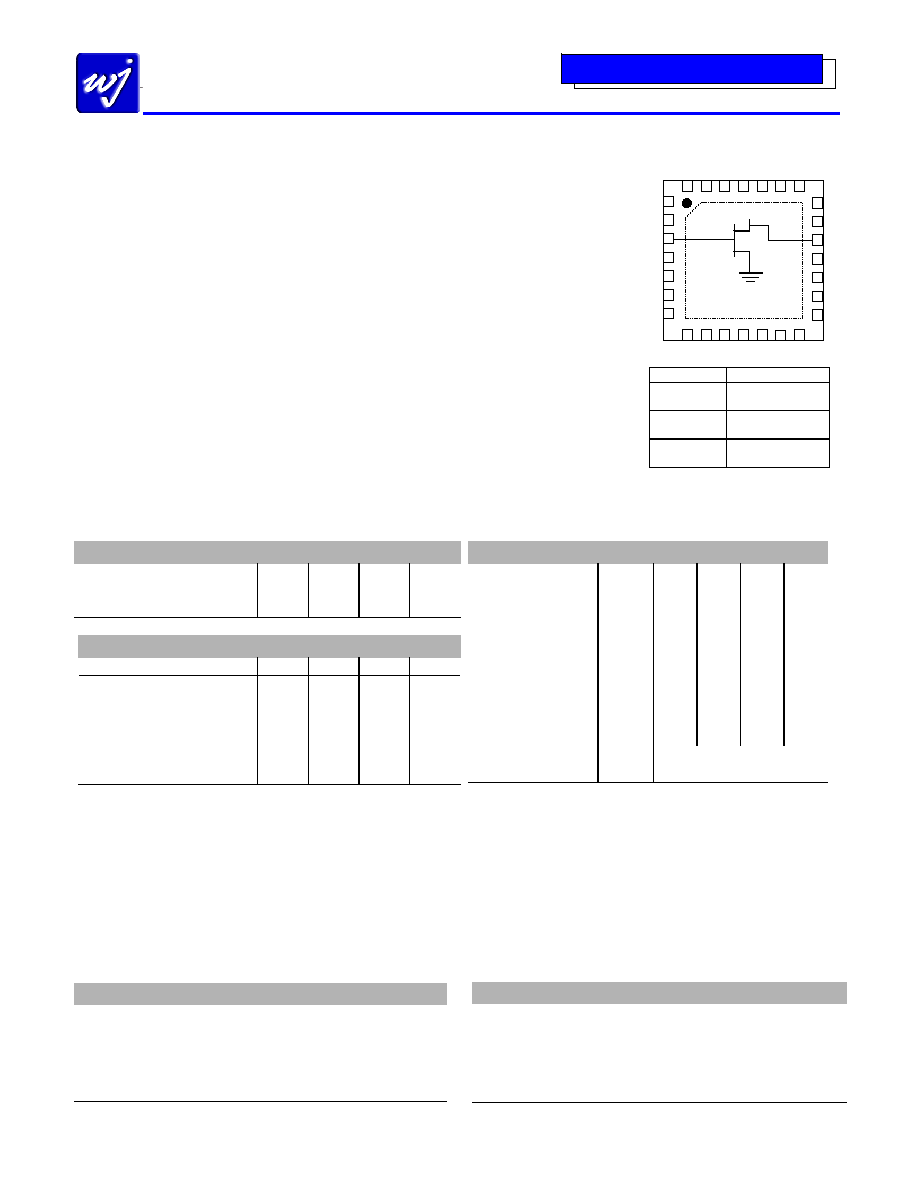
Functional Diagram
Function Pin
No.
Gate /
RF Input
3
Drain /
RF Output
19
Ground
All other pins &
backside copper
Specifications
DC Parameter
Units Min Typ Max
Saturated Drain Current, I
dss
mA
1170
Transconductance, G
m
mS
590
Pinch Off Voltage, V
p
(1)
V
-2.0
RF Parameter
(2)
Units Min Typ Max
Operational Bandwidth
MHz
50
4000
Test Frequency
MHz
800
Small Signal Gain
dB
18
Maximum Stable Gain
dB
24
Output P1dB
dBm
+34
Output IP3
(3)
dBm
+46
Noise Figure
dB
3.5
1. Pinch-off voltage is measured when I
ds
= 4.8 mA.
2. Test conditions unless otherwise noted: T = 25∫C, V
DS
= 9 V, I
DQ
= 450 mA, in a tuned application
circuit with Z
L
= Z
LOPT
, Z
S
= Z
SOPT
(optimized for output power).
3. 3OIP measured with two tones at an output power of +18 dBm/tone separated by 1 MHz. The
suppression on the largest IM3 product is used to calculate the 3OIP using a 2:1 rule.
Absolute Maximum Rating
Parameter
Rating
Operating Case Temperature
-40 to +85
∞C
Storage Temperature
-55 to +125
∞C
DC Power
7.5 W
RF Input Power (continuous)
6 dB above Input P1dB
Drain to Gate Voltage, V
dg
+14
V
Junction Temperature
+220
∞ C
Operation of this device above any of these parameters may cause permanent damage.
Typical Performance
(4)
Parameter
Units
Typical
Frequency MHz
915
1960
2140
2450
Gain
dB 18 13.5 13 12
S11
dB -20 -20 -18 -18
S22
dB -12 -11 -24 -15
Output P1dB
dBm
+34 +33.8 +33.2 +33.5
Output IP3
(3)
dBm
+46
+46.8
+46.6 +46.8
Noise
Figure
dB 3.5 4.5 4.6 4.6
IS-95 Channel Power
@ -45 dBc ACPR
dBm +27.8
+27.3
W-CDMA Ch. Power
@ -45 dBc ACLR
dBm +25
Drain Voltage
(5)
V
+9
Drain Current
(5)
mA
450
4. Typical parameters represent performance in an application circuit.
5. Empirical measurements showed optimal power performance at a drain voltage = 9 volts at 450 mA.
Because the FP31QF is a discrete device, users can choose their own bias configuration. Performance
may vary from the data shown depending on the biasing conditions. To achieve a minimum 1 million
hours MTTF rating, the biasing condition should maintain a junction temperature below 160
∞ C over all
operating temperatures. This can be approximated by (drain voltage) x (drain current) x 17.5
∞ C/W +
(maximum operating temperature).
Ordering Information
Part No.
Description
FP31QF
2-Watt HFET
(Leaded QFN Pkg)
FP31QF-F
2-Watt HFET
(lead-free/RoHS-compliant QFN Pkg)
FP31QF-PCB900
870 ≠ 960 MHz Application Circuit
FP31QF-PCB1900
1930 ≠ 1990 MHz Application Circuit
FP31QF-PCB2140
2110 ≠ 2170 MHz Application Circuit
1
2
3
4
5
6
7
21
20
19
18
17
16
15
28
27
26
25
24
23
22
8
9
10
11
12
13
14
GND
GND
DRAIN /
RF OUT
GND
GND
GND
GND
GND
GND
GATE /
RF IN
GND
GND
GND
GND
GND
GND
GND
GND
GND
GND
GND
GND
GND
GND
GND
GND
GND
GND
Specifications and information are subject to change without notice
WJ Communications, Inc
∑
Phone 1-800-WJ1-4401
∑
FAX: 408-577-6621
∑
e-mail: sales@wj.com
∑
Web site: www.wj.com
November
2004
FP31QF
2-Watt HFET
Product Information
The Communications Edge
TM
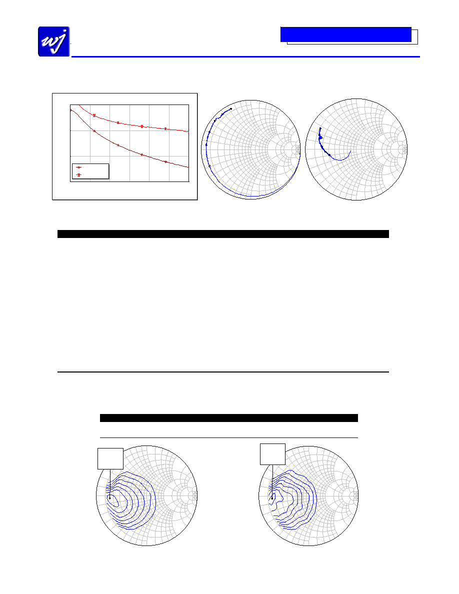
Typical Device Data
S-Parameters (V
DS
= +9 V, I
DS
= 450 mA, T = 25
∞C, calibrated to device leads)
0
0.5
1
1.5
2
2.5
3
Frequency (GHz)
S21, Maximum Stable Gain vs. Frequency
0
10
20
30
S21
,
M
S
G
(
d
B)
DB(|S[2,1]|)
DB(MSG)
0
1.
0
1.
0
-1
.0
10
.
0
10.0
-1
0.
0
5.
0
5.0
-5
.0
2.
0
2.
0
-2
.0
3.0
3.
0
-3
.0
4.
0
4.
0
-4.
0
0.
2
0.
2
-0.
2
0.
4
0.
4
-0
.4
0.
6
0.
6
-0
.6
0.
8
0.
8
-0
.8
S11
Swp Max
6GHz
Swp Min
0.01GHz
0
1.
0
1.
0
-1
.0
10
.0
10.0
-1
0.
0
5.
0
5.0
-5
.0
2.
0
2.
0
-2
.0
3.
0
3.
0
-3
.0
4.
0
4.
0
-4
.0
0.
2
0.
2
-0.
2
0.
4
0.
4
-0
.4
0.
6
0.
6
-0
.6
0.
8
0.
8
-0
.8
S22
Swp Max
6GHz
Swp Min
0.01GHz
Note:
Measurements were made on the packaged device in a test fixture with 50 ohm input and output lines.
The S-parameters shown are the de-embedded data down to the device leads and represents typical performance of the device.
Freq (MHz)
S11 (mag)
S11 (ang)
S21 (mag)
S21 (ang)
S12 (mag)
S12 (ang)
S22 (mag)
S22 (ang)
50 0.985 -21.82 24.458 166.25 0.006 76.01 0.096 -110.34
250 0.936 -88.63 17.968 128.52 0.020 43.34 0.329 -135.13
500 0.913 -128.61 11.520 104.42 0.025 22.03 0.431 -151.01
750 0.899 -148.43 8.132 90.03 0.026 10.75 0.465 -158.3
1000 0.900 -160.54 6.225 79.35 0.026 4.56 0.490 -162.14
1250 0.900 -169.15 4.988 70.50 0.025 0.35 0.514 -163.92
1500 0.900 -176.01 4.125 62.56 0.025 -2.975 0.532 -166.86
1750 0.905 178.53 3.504 55.28 0.024 -4.91 0.560 -168.72
2000 0.909 172.99 3.046 47.93 0.023 -5.54 0.587 -170.95
2250 0.910 168.27 2.656 41.65 0.022 -4.44 0.606 -172.86
2500 0.914 164.14 2.349 34.95 0.021 -1.12 0.629 -175.13
2750 0.914 160.09 2.117 28.98 0.021 5.24 0.656 -177.13
3000 0.915 156.76 1.897 23.31 0.022 12.75 0.671 -179.41
3250 0.922 153.22 1.721 17.69 0.026 23.36 0.695 177.36
3500 0.926 149.22 1.563 11.97 0.034 32.54 0.720 175.05
3750 0.941 144.67 1.433 6.20 0.058 34.08 0.734 171.21
4000 0.943 140.45 1.318 0.98 0.102 23.74 0.768 165.82
Device S-parameters are available for download off of the website at: http://www.wj.com
Load-Pull Data at 1.96 and 2.14 GHz
(V
ds
= 8 V, I
ds
= 500 mA, 25∞C, Z
S
= 50
, calibrated to device pins)
Freq (GHz)
ZS (
)
ZL (
)
Gain (dB)
P1dB (dBm) OIP3 (dBm)
PAE (%)
1.96
5 + j0
8 - j2
18.5
+34
+48
49
2.14
5 - j2
8 - j3
18.0
+34
+48
50
0
1.0
1.
0
-1
.0
10
.
0
10.0
-1
0.
0
5.0
5.0
-5
.0
2.0
2.
0
-2
.0
3.
0
3.
0
-3
.0
4.
0
4.
0
-4.
0
0.
2
0.
2
-0.
2
0.4
0.4
-0.
4
0.
6
0.
6
-0
.6
0.
8
0
.
8
-
0
.
8
P1dB
Swp Max
1.96GHz
Swp Min
1e-009GHz
1.96 GHz
r 8 Ohm
x -2 Ohm
33
32
31
30
29
28
27
0
1.0
1.0
-1.0
10.0
10.0
-1
0.
0
5.0
5.0
-5.
0
2.0
2.
0
-2
.0
3.
0
3.
0
-3
.0
4.
0
4.0
-4
.0
0.2
0.2
-0.
2
0.4
0.
4
-0.
4
0.6
0.
6
-0
.6
0.
8
0
.
8
-
0
.
8
Output IP3
Swp Max
1.96GHz
Swp Min
1e-009GHz
1.96 GHz
r 8 Ohm
x -2 Ohm
48
47
46
45
44
43
42
41
P1dB max (1.96 GHz) = +34 dBm at Z
L
= 8 - j2
OIP3 max (1.96 GHz) = +48 dBm at Z
L
= 8 - j2
1
2
3
4
5
6
1
2
3
4
5
6
Specifications and information are subject to change without notice
WJ Communications, Inc
∑
Phone 1-800-WJ1-4401
∑
FAX: 408-577-6621
∑
e-mail: sales@wj.com
∑
Web site: www.wj.com
November
2004
FP31QF
2-Watt HFET
Product Information
The Communications Edge
TM
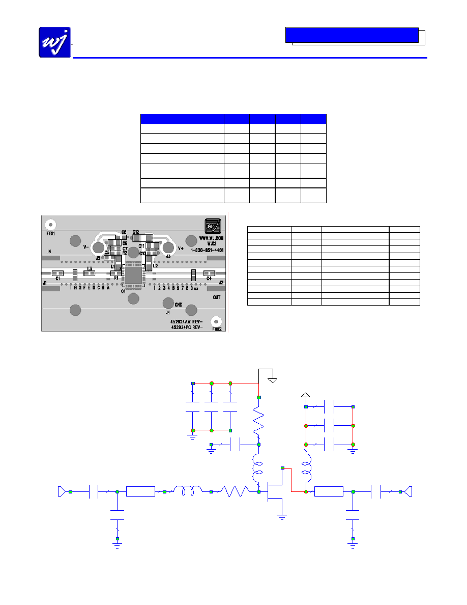
Application Circuit: 870 ≠ 960 MHz (FP31QF-PCB900)
The application circuit is matched for output power.
Typical RF Performance
Drain Bias = +9 V, I
ds
= 450 mA, 25
∞C
Frequency
MHz
870
915
960
S21 ≠ Gain
dB
18.3
18
17.7
S11 ≠ Input Return Loss
dB
-15
-20
-16
S22 ≠ Output Return Loss
dB
-9.3
-12
-16
Output P1dB
dBm
+33.9
+34
+33.7
Output IP3
(+18 dBm / tone, 1 MHz spacing)
dBm +46
Noise
Figure
dB 3.4 3.5 3.5
IS-95 Channel Power
@ -45 dBc ACPR
dBm +27.8
Circuit Board Material: .014" FR-4 (
r
= 4.6),
4 layers (other layers added for rigidity), .062" total thickness, 1 oz copper
The main microstrip line has a line impedance of 50 .
Bill of Materials
Ref. Desig.
Value
Part style
Size
C1, C4, C8, C10
100 pF
Chip capacitor
0603
C2, C3
4.7 pF
Chip capacitor
0603
C6, C11
0.018
µF
Chip capacitor
0805
C7
1000 pF
Chip capacitor
0603
C12
0.1
µF
Chip capacitor
1206
L1, L2
27 nH
Wirewound chip inductor
0805
L3
3.3 nH
Multilayer chip inductor
0603
R1 10
Chip
resistor
0603
R2 51
Chip
resistor
0603
Q1
FP31QF
WJ 2W HFET
QFN 6x6
C5
Do Not Place
∑
The C2 and C3 placements are at silk screen markers, "H" and "9.5", respectively.
∑
The via hole spacing along the main microstrip line is .040".
∑
The distance from the edge of the FP31QF to the closer edge of L3 is .305".
∑
The transmission line lengths shown in the schematic are from the FP31QF
device edge to the component edge.
RES
R=
ID=
10 Ohm
R1
CAP
C=
ID=
10 0 pF
C1
IND
L =
ID=
2 7 nH
L2
CAP
C =
ID =
10 0 pF
C10
CAP
C=
ID=
1.8e4 pF
C11
CAP
C=
ID=
1e5 pF
C12
CAP
C=
ID=
100 pF
C4
CA P
C=
ID=
1.8e4 pF
C8
CA P
C=
ID=
100 pF
C6
CAP
C =
ID =
1000 pF
C7
CAP
C=
ID=
4.7 pF
C3
IND
L=
ID=
27 nH
L1
RES
R=
ID=
51 Ohm
R2
CAP
C=
ID=
DNP pF
C5
IND
L=
ID=
3.3 nH
L3
TLINP
F0=
Loss=
Eeff=
L=
Z0=
ID=
0 MHz
0
3.46
520 mil
50 Ohm
TL2
CAP
C=
ID=
4.7 pF
C2
TL INP
F0 =
Loss=
Eeff=
L=
Z0 =
ID=
0 MHz
0
3.46
500 mil
50 Ohm
TL1
1
2
SUB CKT
NET=
ID=
"FP31QF"
Q1
P ORT
Z=
P =
50 Ohm
1
P ORT
Z=
P =
50 Ohm
2
-Vgg
Vds=9V @ 450 mA
C2
C3

Specifications and information are subject to change without notice
WJ Communications, Inc
∑
Phone 1-800-WJ1-4401
∑
FAX: 408-577-6621
∑
e-mail: sales@wj.com
∑
Web site: www.wj.com
November
2004
FP31QF
2-Watt HFET
Product Information
The Communications Edge
TM
FP31QF-PCB900 Application Circuit Performance Plots
S11 vs. Frequency
-30
-25
-20
-15
-10
-5
0
860
880
900
920
940
960
Frequency (MHz)
S11
(
dB
)
-40c
+25c
+85c
S21 vs. Frequency
15
16
17
18
19
20
860
880
900
920
940
960
Frequency (MHz)
S21
(
dB
)
-40c
+25c
+85c
S22 vs. Frequency
-30
-25
-20
-15
-10
-5
0
860
880
900
920
940
960
Frequency (MHz)
S22
(
dB
)
-40c
+25c
+85c
P1dB vs. Frequency
26
28
30
32
34
36
860
880
900
920
940
960
Frequency (MHz)
P1dB
(
dBm
)
-40c
+25c
+85c
Noise Figure vs. Frequency
0
1
2
3
4
5
6
860
880
900
920
940
960
Frequency (MHz)
NF
(
dB
)
-40c
+25c
+85c
ACPR vs. Channel Power
IS-95, 9 Ch. Forward, ±885 kHz offset, 30 kHz Meas BW
-70
-60
-50
-40
22
23
24
25
26
27
28
29
Output Channel Power (dBm)
ACPR
(
dBc
)
-40 C
+25 C
+85 C
freq = 915 MHz
OIP3 vs. Temperature
40
42
44
46
48
50
-40
-15
10
35
60
85
Temperature (∞C)
OIP3
(
dBm
)
freq = 915, 916 MHz
+18 dBm / tone
IMD products vs. Output Power
fundamental frequency = 915 MHz, 916 MHz; Temp = +25∞ C
-100
-80
-60
-40
-20
4
8
12
16
20
24
28
Output Power (dBm)
IMD
p
roduc
ts
(
dBm
)
IMD_Low
IMD_High
OIP3 vs. Output Power
fundamental frequency = 915 MHz, 916 MHz; Temp = +25∞ C
30
35
40
45
50
4
8
12
16
20
24
28
Output Power (dBm)
OIP3
(
dBm
)
Output Power / Gain vs. Input Power
frequency = 915 MHz, Temp = -40∞ C
10
12
14
16
18
20
-4
0
4
8
12
16
20
Input Power (dBm)
Gain
(
dB
)
16
20
24
28
32
36
Out
p
ut P
o
wer
(
dBm
)
Output Power
Gain
Output Power / Gain vs. Input Power
frequency = 915 MHz, Temp = +25∞ C
10
12
14
16
18
20
-4
0
4
8
12
16
20
Input Power (dBm)
Gain
(
dB
)
16
20
24
28
32
36
Out
p
ut P
o
wer
(
dBm
)
Output Power
Gain
Output Power / Gain vs. Input Power
frequency = 915 MHz, Temp = +85∞ C
10
12
14
16
18
20
-4
0
4
8
12
16
20
Input Power (dBm)
Gain
(
dB
)
16
20
24
28
32
36
Out
p
ut P
o
wer
(
dBm
)
Output Power
Gain

Specifications and information are subject to change without notice
WJ Communications, Inc
∑
Phone 1-800-WJ1-4401
∑
FAX: 408-577-6621
∑
e-mail: sales@wj.com
∑
Web site: www.wj.com
November
2004
FP31QF
2-Watt HFET
Product Information
The Communications Edge
TM
Application Circuit: 1930 ≠ 1960 MHz (FP31QF-PCB1900)
The application circuit is matched for output power.
Typical RF Performance
Drain Bias = +9 V, I
ds
= 450 mA, 25
∞C
Frequency
MHz
1930
1960
1990
S21 ≠ Gain
dB
14
13.8
13.8
S11 ≠ Input Return Loss
dB
-17
-21
-27
S22 ≠ Output Return Loss
dB
-11
-11
-13
Output
P1dB
dBm +33.5 +33.8 +33.8
Output IP3
(+18 dBm / tone, 1 MHz spacing)
dBm +46.8
Noise
Figure
dB 4.3 4.5 4.4
IS-95 Channel Power
@ -45 dBc ACPR
dBm +27.3
Circuit Board Material: .014" FR-4 (
r
= 4.6),
4 layers (other layers added for rigidity), .062" total thickness, 1 oz copper
The main microstrip line has a line impedance of 50 .
Bill of Materials
Ref. Desig.
Value
Part style
Size
C1, C4, C8, C10
22 pF
Chip capacitor
0603
C2 2.2
pF
Chip
capacitor
0603
C3 2.0
pF
Chip
capacitor
0603
C6, C11
0.018
µF
Chip capacitor
0805
C7
1000 pF
Chip capacitor
0603
C12
0.1
µF
Chip capacitor
1206
L1, L2
12 nH
Wirewound chip inductor
0805
L3
4.7 nH
Multilayer chip inductor
0603
R1 5.1
Chip
resistor
0603
R2 51
Chip
resistor
0603
Q1
FP31QF
WJ 2W HFET
QFN 6x6
C5
Do Not Place
∑
The C2 and C3 placements are at silk screen markers, "B" and "3", respectively.
∑
The via hole spacing along the main microstrip line is .040".
∑
The distance from the edge of the FP31QF to the closer edge of L3 is .305".
∑
The transmission line lengths shown in the schematic are from the FP31QF
device edge to the component edge.
RES
R=
ID=
5 Ohm
R1
CAP
C=
ID=
22 pF
C1
IND
L =
ID=
1 2 nH
L2
CAP
C =
ID =
22 pF
C10
CAP
C=
ID=
1.8e4 pF
C11
CAP
C=
ID=
1e5 pF
C12
CAP
C=
ID=
2 2 pF
C4
CA P
C=
ID=
1.8e4 pF
C8
CA P
C=
ID=
2 2 pF
C6
CAP
C =
ID =
1000 pF
C7
CAP
C=
ID=
2 pF
C3
IND
L=
ID=
12 nH
L1
RES
R=
ID=
51 Ohm
R2
CAP
C=
ID=
DNP pF
C5
IND
L=
ID=
4.7 nH
L3
TLINP
F0=
Loss=
Eeff=
L=
Z0=
ID=
0 MHz
0
3.46
200 mil
50 Ohm
TL2
CA P
C=
ID=
2.2 pF
C2
TLINP
F0=
Loss =
Eeff =
L=
Z0=
ID =
0 MHz
0
3.46
190 mil
50 Ohm
TL1
1
2
SUB CKT
NET=
ID=
"FP31QF"
Q1
P ORT
Z=
P =
50 Ohm
1
P ORT
Z=
P =
50 Ohm
2
-Vgg
Vds=9V @ 450 mA
C2
C3