
This document contains information on a new product.
Specifications and information are subject to change without notice
WJ Communications, Inc
∑
Phone 1-800-WJ1-4401
∑
FAX: 408-577-6621
∑
e-mail: sales@wj.com
∑
Web site: www.wj.com
July
2003
VG111
PCS/UMTS-band Variable Gain Amplifier
Product Information
The Communications Edge
TM
Product Features
∑
1800 ≠ 2200 MHz bandwidth
∑
29 dB Attenuation Range
∑
+40 dBm Output IP3
∑
+21 dBm P1dB
∑
Constant IP3 & P1dB over
attenuation range
∑
Single voltage supply
∑
6x6 mm 28-pin QFN package
∑
MTTF > 100 years
Applications
∑
Xmit & Rcv AGC circuitry for
mobile infrastructure
Product Description
The VG111 is a PCS / UMTS-band high dynamic
range variable gain amplifier (VGA) packaged in a
6x6 mm surface-mount package. The +21 dBm
output compression point and +40 dBm output
intercept point of the amplifier are maintained over
the entire attenuation range, making the VG111 ideal
for use in transmitter and receiver AGC circuits and
as a variable gain stage following an LNA in high
dynamic range receiver front ends.
Superior thermal design allows the product to have a
minimum MTTF rating of 100 years at a mounting
temperature of +85∫ C. All devices are 100% RF &
DC tested and packaged on tape and reel for
automated surface-mount assembly.
Functional Diagram
Function Pin
No
Gain Control
5
No Connect
7, 19, 21
RF Input
11
RF Output / DC bias
25
Ground
All other pins
Backside copper
Specifications
Parameter
Units
Min
Typ
Max
Conditions
Frequency
Range
MHz 1800 1900 2100 2200
See
note
1
Gain at min. attenuation
dB
12
14
14
Input Return Loss
dB
9
12
Output Return Loss
dB
9
12
Output
P1dB
dBm +21.5 +21
Output IP3
dBm
+40
+37.5
See note 2
Noise Figure at min. attenuation
dB
4.0
4.1
V
CTRL
= 0 V
Gain Variation Range
dB
29
30
See note 3
Gain Variation Control Voltage, V
CTRL
V
0
4.5
Group
Delay
ns 0.6
Supply Voltage
V
+5
Operating Amplifier Current Range
mA
120
150
180
Pin 25
Gain Control Pin Current Range
mA
0
25
Pin 5 draws no current at maximum gain
Thermal Resistance
∞
C / W
59
Junction Temperature
∞
C
160
See
note
4
Test conditions unless otherwise noted.
1. T = 25∫C, Vdd = +5 V, Frequency = 800 MHz in an application circuit.
2. 3OIP measured with two tones at an output power of +10 dBm/tone separated by 10 MHz. The suppression on the largest IM3 product is used to calculate the 3OIP using a 2:1 rule.
3. The gain variation range is measured with 16 mA of current on gain control pin 5.
4. The junction temperature ensures a minimum MTBF rating of 1 million hours of usage.
Absolute Maximum Rating
Ordering Information
Parameter
Rating
Part No.
Description
Operating Case Temperature
-40 to +85
∞
C
VG111
PCS/UMTS-band Variable Gain Amplifier
Storage Temperature
-55 to +125
∞
C
VG111-PCB1900 1.8 ≠ 2.0 GHz Fully Assembled Application Board
Amplifier Supply Voltage (pin 25)
+6 V
VG111-PCB2100 2.0 ≠ 2.2 GHz Fully Assembled Application Board
Attenuation Control Voltage
+5.5 V
RF Input Power (continuous)
+12 dBm
Junction Temperature
+220
∞
C
Operation of this device above any of these parameters may cause permanent damage.
N/
C
GND
Vc
t
r
l
GND
GND
GND
GND
8
9
10
11
12
13
14
28
27
26
25
24
23
22
7
6
5
4
3
2
1
15
16
17
18
19
20
21
GND
GND
GND
RF OUT
GND
GND
GND
GND
GND
GND
RF IN
GND
GND
GND
GND
GND
GND
GND
N/
C
GND
N/
C
Variable
Attenuator
Amp
This document contains information on a new product.
Specifications and information are subject to change without notice
WJ Communications, Inc
∑
Phone 1-800-WJ1-4401
∑
FAX: 408-577-6621
∑
e-mail: sales@wj.com
∑
Web site: www.wj.com
July
2003
VG111
PCS/UMTS-band Variable Gain Amplifier
Product Information
The Communications Edge
TM
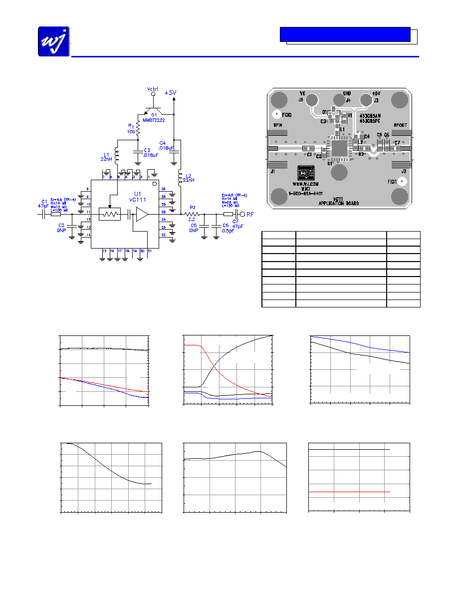
Application Circuit: 1.8 ≠ 2.0 GHz (VG111-PCB1900)
∑
Pins 7, 19, and 21 should not be connected.
∑
The amplifier is biased through Pin 25 and should be connected directly into a voltage regulator.
∑
DNP represents Do Not Place.
∑
Distances are shown from the edge-to-edge for the land pattern.
Circuit Board Material: .014" FR-4, 4 layers, .062" total thickness
Bill of Materials
Ref. Des.
Description
Size
C1, C7
47 pF Chip Capacitor
0603
C2, C5
Do Not Place
C3, C4
0.01
µ
F Chip Capacitor
0603
C6
0.5 pF Chip Capacitor
0603
L1, L2
22 nH Chip Inductor
0603
R1
100
Chip Resistor
0603
R2
2.2
Chip Resistor
0603
Q1 MMBT2222
Motorola
Transistor
SOT-23
U1
VG111 Variable Gain Amplifier
QFN 6x6
S-Parameters
Attenuation Control Voltage = 0 V, 25∞C
6
8
10
12
14
16
1800
1850
1900
1950
2000
Frequency (MHz)
S21 (dB)
-20
-15
-10
-5
0
5
Return Loss (dB)
S22
S11
S21
S11, S22, S21 vs Gain Control Voltage
frequency = 1900 MHz, 25∞C
-20
-10
0
10
20
0
1
2
3
4
5
Gain Control Voltage (V)
Magnitude (dB)
-30
-20
-10
0
10
Normalized Gain (dB)
Gain
S22
S11
Normalized to the maximum
gain level of 14 dB
Normalized Gain
Gain Flatness
25∞C
-2.0
-1.5
-1.0
-0.5
0.0
-25
-20
-15
-10
-5
0
Normalized Gain (dB)
Flatness (dB)
f = 1.93 - 1.99 GHz
f = 1.85 - 1.91 GHz
Normalized to the maximum gain level of 14 dB
Phase Shift vs. Normalized Gain
frequency = 1900 MHz, 25∞C
-30
-25
-20
-15
-10
-5
0
-30
-25
-20
-15
-10
-5
0
Normalized Gain (dB)
Normalized Phase (deg)
Output Intercept Point vs. Output Power
frequency = 1900 MHz, 25∞C
20
25
30
35
40
-5
0
5
10
15
Output Power (dBm)
OIP3 (dBm)
OIP3 / P1dB vs. Normalized Gain
frequency = 1900 MHz, Pout = +10 dBm, 25∞C
15
20
25
30
35
40
-20
-15
-10
-5
0
Normalized Gain (dB)
Magnitude (dBm)
P1dB
OIP
Normalized to the maximum gain level of 14 dB
This document contains information on a new product.
Specifications and information are subject to change without notice
WJ Communications, Inc
∑
Phone 1-800-WJ1-4401
∑
FAX: 408-577-6621
∑
e-mail: sales@wj.com
∑
Web site: www.wj.com
July
2003
VG111
PCS/UMTS-band Variable Gain Amplifier
Product Information
The Communications Edge
TM
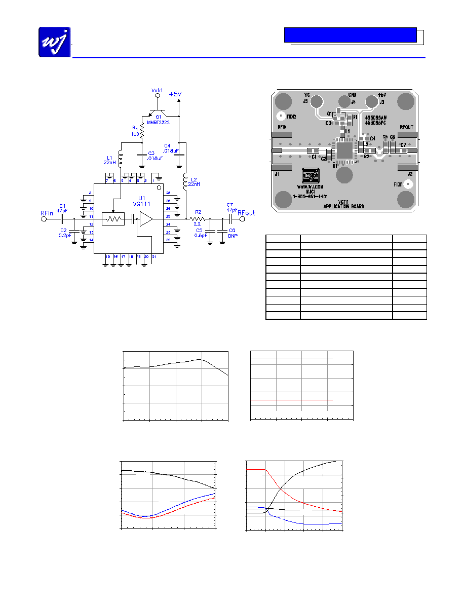
Application Circuit: 2.0 ≠ 2.2 GHz (VG111-PCB2100)
∑
Pins 7, 19, and 21 should not be connected.
∑
The amplifier is biased through Pin 25 and should be connected directly into a voltage regulator.
∑
DNP represents Do Not Place.
∑
Distances are shown from the edge-to-edge for the land pattern.
Circuit Board Material: .014" FR-4, 4 layers, .062" total thickness
Bill of Materials
Ref. Des.
Description
Size
C1, C7
47 pF Chip Capacitor
0603
C2
0.2 pF Chip Capacitor
0603
C3, C4
0.01
µ
F Chip Capacitor
0603
C5
0.6 pF Chip Capacitor
0603
C6
Do Not Place
L1, L2
22 nH Chip Inductor
0603
R1
100
Chip Resistor
0603
R2
2.2
Chip Resistor
0603
Q1 MMBT2222
Motorola
Transistor
SOT-23
U1
VG111 Variable Gain Amplifier
QFN 6x6
Output Intercept Point vs. Output Power
frequency = 2140 MHz, 25∞C
20
25
30
35
40
-5
0
5
10
15
Output Power (dBm)
OIP3 (dBm)
OIP3 / P1dB vs. Normalized Gain
frequency = 2140 MHz, Pout = +10 dBm, 25∞C
15
20
25
30
35
40
-20
-15
-10
-5
0
Normalized Gain (dB)
Magnitude (dBm)
P1dB
OIP
Normalized to the maximum gain level of 14 dB
S-Parameters
Attenuation Control Voltage = 0 V, 25∞C
6
8
10
12
14
16
2000
2100
2200
2300
Frequency (MHz)
Gain
(
dB
)
-20
-15
-10
-5
0
5
Return Loss
(
dB
)
Gain
S22
S11
S11, S22, S21 vs Gain Control Voltage
frequency = 2140 MHz, 25∞C
-30
-20
-10
0
10
20
0
1
2
3
4
5
Gain Control Voltage (V)
Ma
g
nitude
(
dB
)
-30
-20
-10
0
10
Normalized Gain
(
dB
)
Gain
S22
S11
Normalized to the maximum gain
level of 14 dB
Normalized Gain
This document contains information on a new product.
Specifications and information are subject to change without notice
WJ Communications, Inc
∑
Phone 1-800-WJ1-4401
∑
FAX: 408-577-6621
∑
e-mail: sales@wj.com
∑
Web site: www.wj.com
July
2003
VG111
PCS/UMTS-band Variable Gain Amplifier
Product Information
The Communications Edge
TM
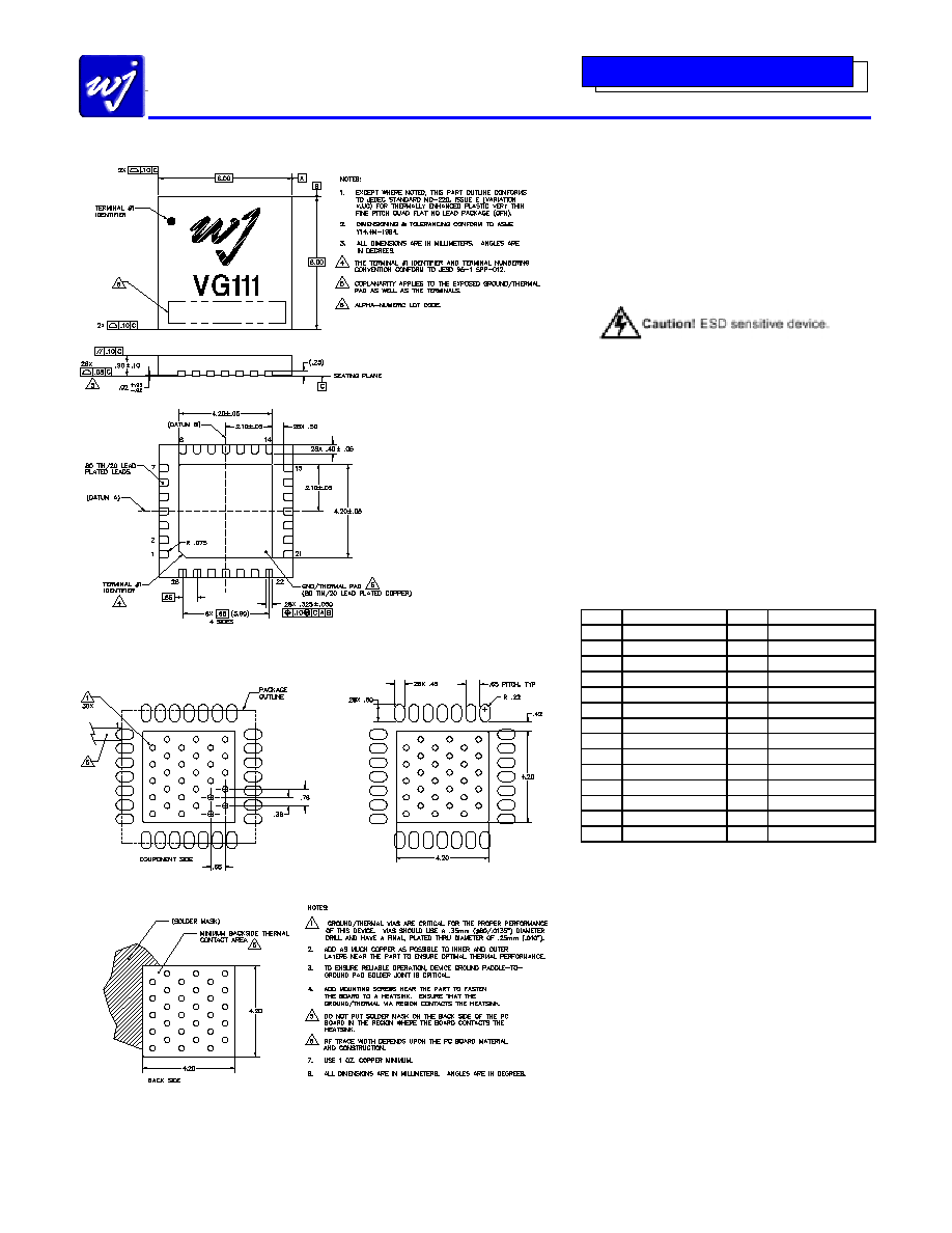
Outline Drawing
Mounting Configuration / Land Pattern
Product Marking
The component will be lasermarked with a "VG111"
designator with a four-digit alphanumeric lot code on
the top surface of the package. Tape and reel
specifications for this part will be located on the
website in the "Application Notes" section.
ESD / MSL Information
ESD Classification: Class 1B
Value:
Passes 600 V
Test:
Human Body Model (HBM)
Standard:
JEDEC Standard JESD22-A114
ESD Classification: Class IV
Value:
Passes 1000 V
Test:
Charged Device Model (CDM)
Standard:
JEDEC Standard JESD22-C101
MSL Rating:
Level 1 at +250
∞
C convection reflow
Standard:
JEDEC Standard J-STD-020B
Functional Pin Layout
Pin FUNCTION Pin FUNCTION
1 GND 15 GND
2 GND 16 GND
3 GND 17 GND
4 GND 18 GND
5
Gain control pin
19
N/C
6 GND 20 GND
7 N/C 21 N/C
8 GND 22 GND
9 GND 23 GND
10 GND 24 GND
11
RF Input
25
RF Output / Bias
12 GND 26 GND
13 GND 27 GND
14 GND 28 GND