 | –≠–ª–µ–∫—Ç—Ä–æ–Ω–Ω—ã–π –∫–æ–º–ø–æ–Ω–µ–Ω—Ç: WM0832 | –°–∫–∞—á–∞—Ç—å:  PDF PDF  ZIP ZIP |
Lutton Court, Bernard Terrace, Edinburgh EH8 9NX, UK
Tel: +44 (0) 131 667 9386 Fax: +44 (0) 131 667 5176
email: admin@wolfson.co.uk
www: http://www.wolfson.co.uk
Wolfson Microelectronics
Production Data data sheets contain final
specifications current on publication date. Supply
of products conforms to Wolfson Microelectronics
standard terms and conditions.
© 1996 Wolfson Microelectronics
Production Data
Sept 1996 Rev 2.1
8-Bit ADCs with Serial Interface and
Differential or Dual Inputs
Description
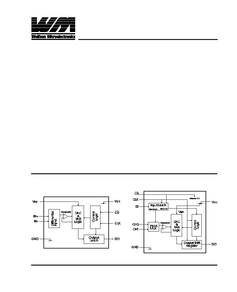
WM0831 and WM0832 are 8-bit analogue to digital
converters (ADC) with serial I/O interfaces, providing a
choice of input configurations in 8-pin SO or DIP packages.
WM0831 has a differential input, also configurable as a
single ended input. A-D conversion results are serially
output on Data Out (DO) under the control of clock and chip
select inputs. The device has a separate voltage reference
input.
WM0832's two input multiplexer is configurable via the Data
In (DI) serial input, as two single ended inputs or a single
differential input. The voltage reference operates
ratiometrically and is internally connected to the VCC pin.
Conversion is initiated by bringing and holding chip select
low while providing a clock input. With WM0831's fixed
input configuration, the conversion result is output at DO on
the clock's falling edges in MSB to LSB order.
With WM0832's configurable input multiplexer, data is input
to DI on the rising edges of the clock to setup the Mux and
initiate conversion. Conversion results appear serially at
DO on the falling edges of the clock, first in MSB to LSB
order, and then repeated in LSB to MSB order.
WM0831/2 operate on 5V or 3.3V supply voltages and are
available in small outline and DIP packages for commercial
(0 to 70
o
C) and industrial (-40 to 85
o
C) temperature ranges.
Features
∑
Functionally Equivalent to National Semiconduc-
tor ADC0831 and ADC0832
∑
WM0831: Differential or single ended input
∑
WM0832: Two single ended inputs or a single
differential input
∑
Ratiometric reference input (fixed for WM0832)
∑
Serial I/O interface
∑
Input range 0 to Vcc with Vcc Reference
∑
8 pin package, SO or DIP
∑
5V and 3.3V variants
∑
Total Unadjusted Error: ± 1 LSB
∑
8-bit resolution
∑
32
µ
µ
µ
µ
µ
s conversion time at fclock = 250 kHz
Applications
∑
Embedding with remote sensors
∑
Equipment health monitoring
∑
Automotive
∑
Industrial control
Block Diagrams
WM0831
WM0832
GND
CH0
CH1
DI
CLK
CS
DO
Vcc
V
REF
Start Conv
Mux Select
Input Latch
Internal CS
Control
Logic
Output Shift
Register
Comparator
WM0832
DAC
&
SAR
Logic
Input
MUX
Control
Logic
Output
Latch
Comparator
WM0831
DAC
&
SAR
Logic
Differential
Input
GND
IN+
IN-
V
REF
CLK
CS
DO
Vcc
WM0831, WM0832

Wolfson Microelectronics
2
WM0831, WM0832
Ordering Information
Pin Configuration
Top View
8 pin P (DIP) and D (SO) packages
WM0831
WM0832
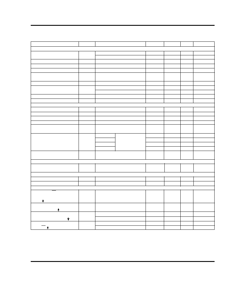
Absolute Maximum Ratings
(note 1)
Supply Voltage, Vcc (note 2) . . . . . . . . . . . 6.5 V
Input voltage range:
Digital Inputs . . . . GND - 0.3 V, VCC + 0.3 V
Analogue inputs . . . GND - 0.3 V, VCC + 0.3 V
Input current, any pin (note 3) . . . . . . ± 5 mA
Total Input current for package . . . . . . ± 20 mA
Operating temperature range, TA . . . . T
MIN
to T
MAX
WM083_C_ (C suffix) . . . . . . . . . 0
o
C to +70
o
C
WM083_I_ (I suffix) . . . . . . . . . . -40
o
C to +85
o
C
Storage Temperature . . . . . . . . - 65
o
C to +150
o
C
Soldering Information:
Lead Temperature 1.6 mm (1/16) from case
for 10 seconds: D or P package . . . . . . . 260
o
C
Recommended Operating Conditions (5V)
SYMBOL
MIN
NOMINAL MAX
UNIT
Supply voltage
V
CC
4.5
5
5.5
V
High level input voltage
V
IH
2
V
Low level input voltage
V
IL
0.8
V
Clock frequency
f
clock
10
600
KHz
Clock duty cycle (see Note 4)
D
clk
40
60
%
Pulse duration CS high
t
wH(CS)
220
ns
Operating free-air temperature
C suffix
T
A
0
70
o
C
I Suffix
T
A
-40
85
DEVICE
TEMP. RANGE
PACKAGE
WM0831CP
0
o
C to 70
o
C
8 pin plastic DIP
WM0831CD
0
o
C to 70
o
C
8 pin plastic SO
WM0831IP
-40
o
C to 85
o
C
8 pin plastic DIP
WM0831ID
-40
o
C to 85
o
C
8 pin plastic SO
WM0832CP
0
o
C to 70
o
C
8 pin plastic DIP
WM0832CD
0
o
C to 70
o
C
8 pin plastic SO
WM0832IP
-40
o
C to 85
o
C
8 pin plastic DIP
WM0832ID
-40
o
C to 85
o
C
8 pin plastic SO
DEVICE
TEMP. RANGE
PACKAGE
WM0831LCP
0
o
C to 70
o
C
8 pin plastic DIP
WM0831LCD
0
o
C to 70
o
C
8 pin plastic SO
WM0831LIP
-40
o
C to 85
o
C
8 pin plastic DIP
WM0831LID
-40
o
C to 85
o
C
8 pin plastic SO
WM0832LCP
0
o
C to 70
o
C
8 pin plastic DIP
WM0832LCD
0
o
C to 70
o
C
8 pin plastic SO
WM0832LIP
-40
o
C to 85
o
C
8 pin plastic DIP
WM0832LID
-40
o
C to 85
o
C
8 pin plastic SO
5V devices
3.3V devices
Wolfson Microelectronics
3
WM0831, WM0832
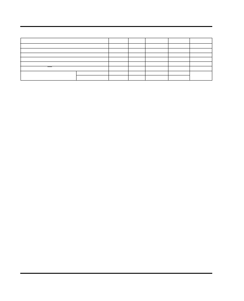
PARAMETER SYMBOL TEST CONDITIONS
MIN
TYP
MAX
UNIT
Digital Inputs
High level output voltage
V
OH
V
CC
= 4.75 V, I
OH
= -360
µ
A
2.4
V
V
CC
= 4.75 V, I
OH
= -10
µ
A
4.5
V
Low level output voltage
V
OL
V
CC
= 5.25 V, I
OH
= 1.6 mA
0.4
V
High level input current
I
IH
V
IH
= 5 V
0.005
1
µ
A
Low level input current
I
IL
V
IL
= 0 V
-0.005
-1
µ
A
High level output (source)
I
OH
V
OH
= 0 V
-6.5
-24
mA
current
Low level output (sink) current
I
OL
V
OL
= V
CC
8
26
mA
High impedance-state
I
OZ
V
O
= 5 V
0.01
3
µ
A
output current (DO)
V
O
= 0 V
-0.01
-3
µ
A
Input capacitance
C
I
5
pF
Output capacitance
C
o
5
pF
Converter and Multiplexer
Total unadjusted error
TUE
V
REF
= 5 V. (note 7)
±1
LSB
Differential Linearity
(note 8)
8
Bits
Supply voltage variation error
V
s(error)
V
CC
= 4.75 V to 5.25 V
±1/16
±1/4
LSB
Common mode error
Differential mode
±1/16
±1/4
LSB
Common mode input voltage
V
ICR
(note 9)
GND-0.05
V
range
V
CC
+0.05
Standby input leakage
I
I(stdby)
On-channel VI = 5 V at ON ch.
1
µ
A
current (note 10)
Off-channel VI = 0 V at OFF ch.
-1
µ
A
On-channel VI = 0 V at ON ch.
-1
µ
A
Off-channel VI = 5 V at OFF ch.
1
µ
A
Conversion time
tconv
Excluding MUX addressing time
8
clock
periods
Reference Inputs
Input resistance to
R
i(REF)
Can only be tested for WM0831
1.3
2.4
5.9
k
reference ladder
Total device
Supply current WM0831
I
CC
0.6
1.25
mA
Supply current WM0832
I
CC
( note 11)
2.5
4.7
mA
Timing Parameters
Setup time, CS low or
t
su
350
ns
WM0832 data valid before
clock
Hold time, WM0832 data
t
h
90
ns
valid after clock
Propagation delay time,
MSB data first. C
L
= 100 pF
1500
ns
output data after clock
t
pd
LSB data first. C
L
= 100 pF
600
ns
Output disable time, DO
t
dis
C
L
= 10 pF, R
L
= 10 k
125
250
ns
after CS
CL = 100 pF, R
L
= 2 k
500
ns
Electrical Characteristics
(5V)
V
cc
= 5V, V
REF
= 5V,f
CLK
= 250KHz, T
A
= T
MIN
to T
MAX
, tr = tf = 20 ns, unless otherwise stated.
Wolfson Microelectronics
4
WM0831, WM0832
Recommended Operating Conditions (3.3V)
SYMBOL
MIN
NOMINAL MAX
UNIT
Supply voltage
V
CC
2.7
3.3
3.6
V
High level input voltage
V
IH
2
V
Low level input voltage
V
IL
0.8
V
Clock frequency (Vcc = 3.3V)
f
clock
10
600
KHz
Clock duty cycle (see Note 4)
D
clk
40
60
%
Pulse duration CS high
t
wH(CS)
220
ns
Operating free-air temperature
C suffix
T
A
0
70
o
C
I Suffix
T
A
-40
85

Wolfson Microelectronics
5
WM0831, WM0832
PARAMETER SYMBOL TEST CONDITIONS
MIN
TYP
MAX
UNIT
Digital Inputs
High level output voltage
V
OH
V
CC
= 3V, I
OH
= -360
µ
A
2.4
V
V
CC
= 3 V, I
OH
= -10
µ
A
2.8
V
Low level output voltage
V
OL
V
CC
= 3V, I
OH
= 1.6 mA
0.4
V
High level input current
I
IH
V
IH
= 3.6 V
0.005
1
µ
A
Low level input current
I
IL
V
IL
= 0 V
-0.005
-1
µ
A
High level output (source)
I
OH
V
OH
= 0 V, T
A
= 25
o
C
6.5
15
mA
current
Low level output (sink) current
I
OL
V
OL
= 0V, T
A
= 25
o
C
8
16
mA
High impedance-state
I
OZ
V
O
= 3.3V, T
A
= 25
o
C
0.01
3
µ
A
output current (DO)
V
O
= 0 V, T
A
= 25
o
C
-0.01
-3
µ
A
Input capacitance
C
I
5
pF
Output capacitance
C
o
5
pF
Converter and Multiplexer
Total unadjusted error
TUE
V
REF
= 3.3 V. (note 7)
±1
LSB
Differential Linearity
(note 8)
8
Bits
Supply voltage variation error
V
s(error)
V
CC
= 3 V to 3.6 V
±1/16
±1/4
LSB
Common mode error
Differential mode
±1/16
±1/4
LSB
Common mode input voltage
V
ICR
(note 9)
GND-0.05
V
range
V
CC
+0.05
Standby input leakage
I
I(stdby)
On-channel VI =3.3V at ON ch.
1
µ
A
current (note 10)
Off-channel VI =0 V at OFF ch.
-1
µ
A
On-channel VI =0 V at ON ch.
-1
µ
A
Off-channel VI =3.3V at OFF ch.
1
µ
A
Conversion time
tconv
Excluding MUX addressing time
8
clock
periods
Reference Inputs
Input resistance to
R
i(REF)
Can only be tested for WM0831
1.3
2.4
5.9
k
reference ladder
Total device
Supply current WM0831
I
CC
0.2
0.75
mA
Supply current WM0832
I
CC
( note 11)
1.5
2.5
mA
Timing Parameters
Setup time, CS low or
t
su
350
ns
WM0832 data valid before
clock
Hold time, WM0832 data
t
h
90
ns
valid after clock
Propagation delay time,
MSB data first. C
L
= 100 pF
200
500
ns
output data after clock
t
pd
LSB data first. C
L
= 100 pF
80
200
ns
Output disable time, DO
t
dis
C
L
= 10 pF, R
L
= 10 k
80
125
ns
after CS
CL = 100 pF, R
L
= 2 k
250
ns
Electrical Characteristics (3.3V)
V
cc
= 3.3V, f
CLK
= 250KHz, T
A
= T
MIN
to T
MAX
, tr = tf = 20 ns, unless otherwise stated.