 | –≠–ª–µ–∫—Ç—Ä–æ–Ω–Ω—ã–π –∫–æ–º–ø–æ–Ω–µ–Ω—Ç: WM0834LCN | –°–∫–∞—á–∞—Ç—å:  PDF PDF  ZIP ZIP |
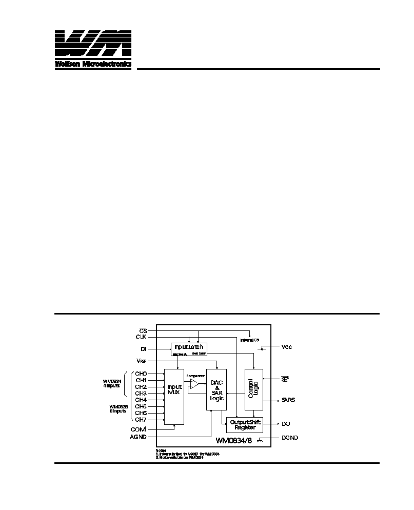
Block Diagram
Lutton Court, Bernard Terrace, Edinburgh EH8 9NX, UK
Tel: +44 (0) 131 667 9386 Fax: +44 (0) 131 667 5176
email: admin@wolfson.co.uk
www: http://www.wolfson.co.uk
Wolfson Microelectronics
Production Data data sheets contain final
specifications current on publication date. Supply
of products conforms to Wolfson Microelectronics
standard terms and conditions.
© 1996 Wolfson Microelectronics
WM0834, WM0838
Production Data
Sept 1996 Rev 2.0
8-Bit ADCs with Serial Interface and
Configurable Input Multiplexer
Description
WM0834 and WM0838 are 8-bit analogue to digital
converters (ADC) with configurable 4-input and 8-input
multiplexers respectively and a serial I/O interface.
Assignment of the multiplexer inputs is configured before
each conversion via the serial data input to give single-ended
or differential operation for the selected inputs. A mixture of
input configurations can be used in the same application.
WM0838 also has a pseudo-differential configuration where
all 8 inputs can be refered to a common input at an arbitrary
voltage.
Serial communcation with WM0834/8 is via Data In (DI) and
Data Out (DO) wires under the control of clock and chip
select inputs. A high output at the SARS pin indicates when
the conversion is in progress. To initiate a conversion chip
enable is held low and data is input to DI on the rising edge
of the clock, comprising, a start bit, and bits to set up the
input configuration and polarity. After a half clock cycle delay
conversion results appear at DO on the falling edge of the
clock, MSB first, concurrently with A-D conversion. This is
followed by the results LSB first, indicated by the falling edge
of SARS. WM0838 has a shift enable (SE) input used to
control the LSB first output on DO.
WM0834/8 operate on 5V and 3.3V supply voltages and
are available in small outline and DIP packages for com-
mercial (0 to 70
O
C) and industrial (-40 to 85
O
C) tempera-
ture ranges.
Features
∑
Functionally Equivalent to National Semiconduc-
tor ADC0834 and ADC0838 without the Internal
Zener Regulator Network
∑
4-input (WM0834) or 8-input (WM0838) MUX
options
∑
Reference input operates ratiometrically or with
a fixed reference
∑
Input range 0 to Vcc with Vcc Reference
∑
5V and 3.3V variants
∑
Total Unadjusted Error: ± 1 LSB
∑
8-bit resolution
∑
Low Power
∑
32
µ
µ
µ
µ
µ
s conversion time at fclock
= 250 kHz
∑
Serial I/O interface
∑
WM0834 packages: 14 pin SO & DIP
WM0838 packages: 20 pin wide-body SO & DIP
Applications
∑
Embedding with remote sensors
∑
Equipment health monitoring
∑
Automotive
∑
Industrial control
CH0
CH1
CH2
CH3
CH4
CH5
CH6
CH7
COM
1
AGND
V
REF
DI
CLK
CS
Notes:
1. Internally tied to AGND for WM0834
2. Not available on WM0834
WM0834
4 Inputs
WM0838
8 Inputs
DO
SARS
DGND
SE
2
Vcc
Input
MUX
Control
Logic
Output Shift
Register
Comparator
Start Conv
Mux Select
WM0834/8
DAC
&
SAR
Logic
Input Latch
Internal CS

Wolfson Microelectronics
2
WM0834, WM0838
Ordering Information
Pin Configuration
Top View
WM0834 : N(DIP) and D (SO) packages
WM0838: N(DIP) and DW (SO) packages
DEVICE
TEMP. RANGE
PACKAGE
WM0834CN
0
o
C to 70
o
C
14 pin plastic DIP
WM0834CD
0
o
C to 70
o
C
14 pin plastic SO
WM0834IN
-40
o
C to 85
o
C
14 pin plastic DIP
WM0834ID
-40
o
C to 85
o
C
14 pin plastic SO
WM0838CN
0
o
C to 70
o
C
20 pin plastic DIP
WM0838CDW
0
o
C to 70
o
C
20 pin plastic SO
WM0838IN
-40
o
C to 85
o
C
20 pin plastic DIP
WM0838IDW
-40
o
C to 85
o
C
20 pin plastic SO
WM0834
WM0838
Absolute Maximum Ratings
(note 1)
Supply Voltage, Vcc (note 2) . . . . . . . . . . . 6.5 V
Input voltage range:
Digital Inputs . . . . GND - 0.3 V, VCC + 0.3 V
Analogue inputs . . . GND - 0.3 V, VCC + 0.3 V
Input current, any pin (note 3) . . . . . . ± 5 mA
Total Input current for package . . . . . . ± 20 mA
Operating temperature range, TA . . . . TMIN to TMAX
WM083_C_ (C suffix) . . . . . . . . . 0
o
C to +70
o
C
WM083_I_ (I suffix) . . . . . . . . . . -40
o
C to +85
o
C
Storage Temperature . . . . . . . . - 65
o
C to +150
o
C
Soldering Information:
Lead Temperature 1.6 mm (1/16) from case
for 10 seconds: D, DW or N package . . . . . . . 260
o
C
Recommended Operating Conditions (5V)
SYMBOL MIN NOMINAL MAX UNIT
Supply voltage
V
CC
4.5
5
5.5
V
High level input voltage
V
IH
2
V
Low level input voltage
V
IL
0.8
V
Clock frequency
f
clock
10
600
KHz
Clock duty cycle (see Note 4)
D
clk
40
60
%
Pulse duration CS high
t
wH(CS)
220
ns
Operating free-air temperature
C suffix
T
A
0
70
o
C
I Suffix
T
A
-40
85
DEVICE
TEMP. RANGE
PACKAGE
WM0834LCN
0
o
C to 70
o
C
14 pin plastic DIP
WM0834LCD
0
o
C to 70
o
C
14 pin plastic SO
WM0834LIN
-40
o
C to 85
o
C
14 pin plastic DIP
WM0834LID
-40
o
C to 85
o
C
14 pin plastic SO
WM0838LCN
0
o
C to 70
o
C
20 pin plastic DIP
WM0838LCDW
0
o
C to 70
o
C
20 pin plastic SO
WM0838LIN
-40
o
C to 85
o
C
20 pin plastic DIP
WM0838LIDW
-40
o
C to 85
o
C
20 pin plastic SO
5V devices
3.3V devices

Wolfson Microelectronics
3
WM0834, WM0838
Electrical Characteristics
(5V)
V
CC
= 5.0V, V
REF
= 5V, f
CLK
= 250 KHz, T
A
= T
MIN
to T
MAX
, tr = tf = 20ns, unless otherwise stated.
PARAMETER
SYMBOL TEST CONDITIONS
MIN
TYP MAX
UNIT
Digital Inputs
High level output voltage
V
OH
V
CC
= 4.75 V, I
OH
= -360 mA
2.4
V
V
CC
= 4.75 V, I
OH
= -10 mA
4.5
V
Low level output voltage
V
OL
V
CC
= 5.25 V, I
OH
= 1.6 mA
0.4
V
High level input current
I
IH
V
IH
= 5 V
0.005
1
µ
A
Low level input current
I
IL
V
IL
= 0 V
-0.005
-1
µ
A
High level output (source)
I
OH
V
OH
= 0 V
-6.5
-24
mA
current
Low level output (sink) current
I
OL
V
OL
= V
CC
8
26
mA
High impedance-state
I
OZ
V
O
= 5 V
0.01
3
µ
A
output current (DO)
V
O
= 0 V
-0.01
-3
µ
A
Input capacitance
C
i
5
pF
Output capacitance
C
o
5
pF
Converter and Multiplexer
Total unadjusted error
TUE
V
REF
= 5 V. (note 7)
±1
LSB
Differential Linearity
(note 8)
8
Bits
Supply voltage variation error
V
s(error)
V
CC
= 4.75 V to 5.25 V
±1/16
±1/4
LSB
Common mode error
Differential mode
±1/16
±1/4
LSB
Common mode input voltage
V
ICR
(note 9)
GND-0.05
V
range
V
CC
+0.05
Standby input leakage
I
I(stdby)
On-channel VI = 5 V at ON ch.
1
µ
A
current (note 10)
Off-channel VI = 0 V at OFF ch.
-1
µ
A
On-channel VI = 0 V at ON ch.
-1
µ
A
Off-channel VI = 5 V at OFF ch.
1
µ
A
Conversion time
tconv
Excluding MUX addressing time
8
clock
periods
Reference Inputs
Input resistance to
R
i(REF)
1.3
2.4
5.9
k
reference ladder
Total device
Supply current
I
CC
0.6
1.25
mA
Timing Parameters
Setup time, CS low or
t
su
350
ns
data valid before clock
Hold time, data valid after
t
h
90
ns
clock
Propagation delay time,
MSB data first. C
L
= 100 pF
1500
ns
output data after clock
t
pd
LSB data first. C
L
= 100 pF
600
ns
Output disable time, DO
t
dis
C
L
= 10 pF, R
L
= 10 k
125
250
ns
after CS
CL = 100 pF, R
L
= 2 k
500
ns
Wolfson Microelectronics
4
WM0834, WM0838
Recommended Operating Conditions (3.3V)
SYMBOL MIN NOMINAL MAX UNIT
Supply voltage
V
CC
2.7
3.3
3.6
V
High level input voltage
V
IH
2
V
Low level input voltage
V
IL
0.8
V
Clock frequency (Vcc = 3.3V)
f
clock
10
600
KHz
Clock duty cycle (see Note 4)
D
clk
40
60
%
Pulse duration CS high
t
wH(CS)
220
ns
Operating free-air temperature
C suffix
T
A
0
70
o
C
I Suffix
T
A
-40
85

Wolfson Microelectronics
5
WM0834, WM0838
Electrical Characteristics
(3.3V)
V
CC
= 3.3V, f
CLK
= 250 KHz, T
A
= T
MIN
to T
MAX
, tr = tf = 20ns, unless otherwise stated.
PARAMETER
SYMBOL TEST CONDITIONS
MIN
TYP MAX
UNIT
Digital Inputs
High level output voltage
V
OH
V
CC
= 3.0 V, I
OH
= -360 mA
2.4
V
V
CC
= 3.0V, I
OH
= -10 mA
2.8
V
Low level output voltage
V
OL
V
CC
=3.0V, I
OH
= 1.6 mA
0.4
V
High level input current
I
IH
V
IH
= 3.6V
0.005
1
µ
A
Low level input current
I
IL
V
IL
= 0 V
-0.005
-1
µ
A
High level output (source)
I
OH
V
OH
= 0 V, T
A
= 25
o
C
6.5
15
mA
current
Low level output (sink) current
I
OL
V
OL
= V
CC
, T
A
= 25
o
C
8
16
mA
High impedance-state
I
OZ
V
O
= 3.3 V, T
A
= 25
o
C
0.01
3
µ
A
output current (DO)
V
O
= 0 V, T
A
= 25
o
C
-0.01
-3
µ
A
Input capacitance
C
i
5
pF
Output capacitance
C
o
5
pF
Converter and Multiplexer
Total unadjusted error
TUE
V
REF
= 3.3 V. (note 7)
±1
LSB
Differential Linearity
(note 8)
8
Bits
Supply voltage variation error
V
s(error)
V
CC
= 3.0 V to 3.6 V
±1/16
±1/4
LSB
Common mode error
Differential mode
±1/16
±1/4
LSB
Common mode input voltage
V
ICR
(note 9)
GND-0.05
V
range
V
CC
+0.05
Standby input leakage
I
I(stdby)
On-channel VI =3.3 V at ON ch.
1
µ
A
current (note 10)
Off-channel VI = 0 V at OFF ch.
-1
µ
A
On-channel VI = 0 V at ON ch.
-1
µ
A
Off-channel VI =3.3V at OFF ch
1
µ
A
Conversion time
tconv
Excluding MUX addressing time
8
clock
periods
Reference Inputs
Input resistance to
R
i(REF)
1.3
2.4
5.9
k
reference ladder
Total device
Supply current
I
CC
0.2
0.75
mA
Timing Parameters
Setup time, CS low or
t
su
350
ns
data valid before clock
Hold time, data valid after
t
h
90
ns
clock
Propagation delay time,
MSB data first. C
L
= 100 pF
500
ns
output data after clock
t
pd
LSB data first. C
L
= 100 pF
200
ns
Output disable time, DO
t
dis
C
L
= 10 pF, R
L
= 10 k
80
ns
after CS
CL = 100 pF, R
L
= 2 k
250
ns