Document Outline
- WM2124
- DESCRIPTION
- FEATURES
- APPLICATIONS
- BLOCK DIAGRAM
- PIN CONFIGURATION
- ORDERING INFORMATION
- PIN DESCRIPTION
- ABSOLUTE MAXIMUM RATINGS
- RECOMMENDED OPERATINGCONDITIONS
- ELECTRICAL CHARACTERISTICS
- DYNAMIC PERFORMANCE
- PGA SPECIFICATIONS
- TIMING REQUIREMENTS
- SERIAL INTERFACE TIMING
- TIMING OPTIONS
- TIMING DIAGRAMS
- OUTPUT DATA FORMAT
- TYPICAL CHARACTERISTICS
- DEVICE OPERATION
- INTRODUCTION
- SAMPLE AND HOLD AMPLIFIER
- ANALOGUE INPUT,DIFFERENTIAL CONNECTION
- DC-COUPLED DIFFERENTIAL ANALOGUE INPUT CIRCUIT
- AC-COUPLED DIFFERENTIAL ANALOGUE INPUT CIRCUIT
- ANALOGUE INPUT,SINGLE ENDED CONFIGURATION
- REFERENCE TERMINALS
- DIGITAL INPUTS
- DIGITAL OUTPUTS
- LAYOUT,DECOUPLINGAND GROUNDING RULES
- SERIAL INTERFACE
- NOTES
- PACKAGE DIMENSIONS
- IMPORTANT NOTICE
WM2124
Dual 10-bit 40MSPS ADC
WOLFSON MICROELECTRONICS plc
www.wolfsonmicro.com
Advance Information, January 2003, Rev 1.2
Copyright
2003 Wolfson Microelectronics plc
DESCRIPTION
The WM2124 is a dual channel 10-bit 40MSPS ADC which
consumes only 275mWfrom a single 3.3V supply.
The
device is optimised for communications applications that
require close matching between channels and a wide input
bandwidth.
Input
signals
are
differential
for
improved
noise
performance.
Both A and B input channels are sampled
simultaneously and are processed through matched signal
paths of programmable gain amplifier (PGA) and 10-bit
multistage pipeline ADC. A number of different input clock /
output data formats are supported including 20-bits wide at
the sampling rate or 10-bits wide at twice the sampling rate,
with additional clock outputs supplied by the device to latch
the output data.
System
design
and
power
requirements
are
further
simplified by the provision of an on-chip precision voltage
reference. Alternatively, external references can be used if
higher precision references are required.
The device is programmed via a 3-wire serial interface
which allows control of PGA gain setting (0 to 18dB range),
clock / output data formatting, powerdown control and
binary or two's complement number formatting.
FEATURES
�
Two 10-bit resolution ADCs
�
40MSPS conversion rate
�
Simultaneous sampling differential input PGAs with 0 to
18dB gain
�
Programmable clock / output data formats
-
10-bit multiplexed or 20-bit wide output
-
Input clock at sample rate or twice sample rate for
multiplexed output
-
Output clocks for output data sampling
�
Precision internal voltage references
�
Programmable via 3-wire serial interface
�
Wide input bandwidth � 300MHz
�
Low power � 275mWtypical at 3.3V supplies
�
Powerdown mode to less than 1mW
�
48-pin TQFP package
APPLICATIONS
�
I/Q demodulation for
-
Wireless Local Loop (WLL)
-
Set Top Box (STB)
-
Cable Modem
�
IF and Baseband Digitisation
�
Test Instrumentation
�
Medical Imaging
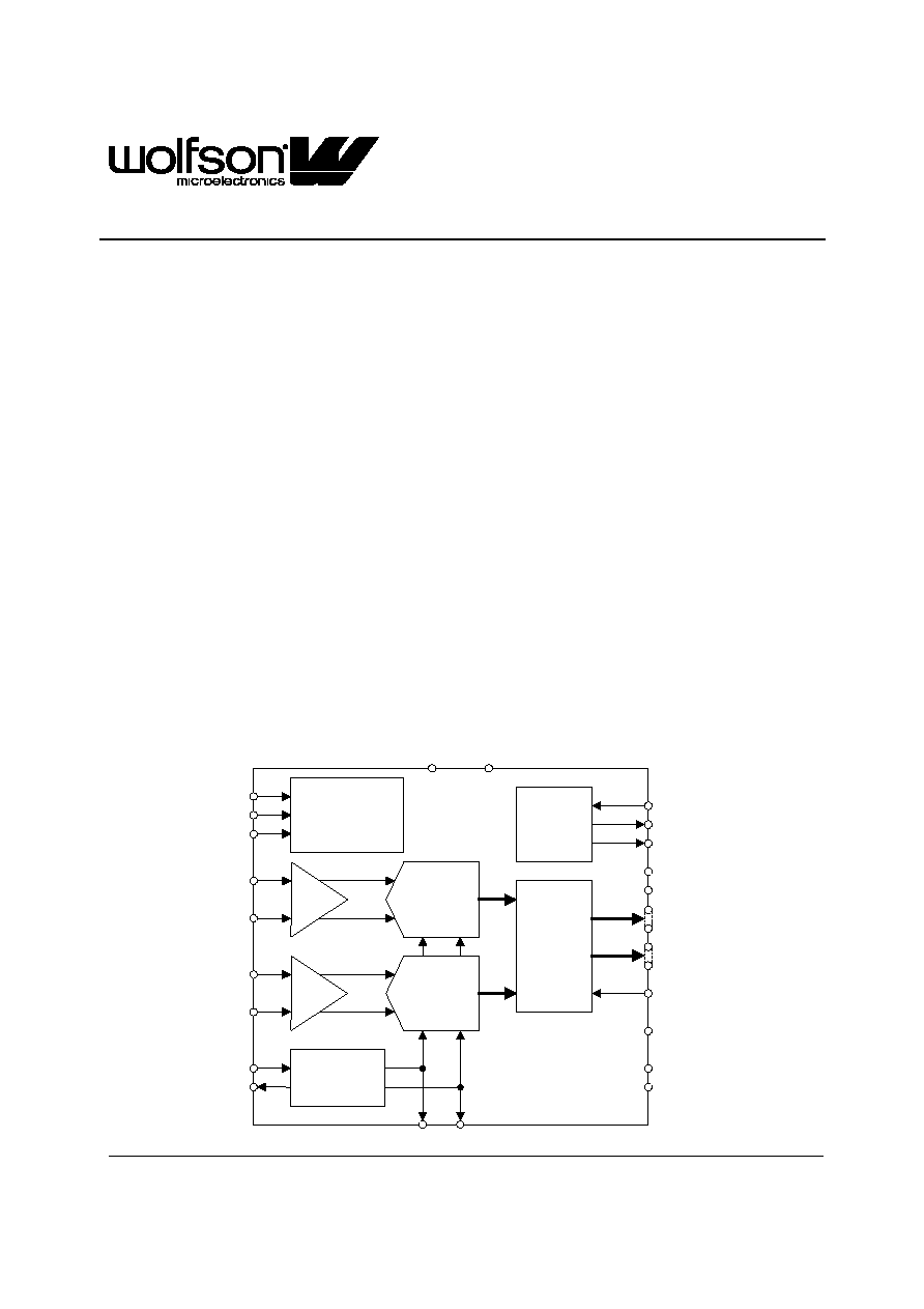
BLOCK DIAGRAM
WM2124
AP
PRECISION
REFERENCE
CIRCUITS
AN
DA[9:0]
AVSS
AVDD
REFT
REFB
STBY
DVSS
DVDD
TIMING
CONTROL
COUTB
PWDN_REF
BP
+
-
BN
+
-
OEB
DB[9:0]
COUT
CLK
DRVSS
DRVDD
CML
CONFIGURATION
CONTROL
CSB
SCLK
SDI
PGA
PGA
10-Bit
ADC
10-Bit
ADC
DATA
OUTPUT
FORMAT
AND
OUTPUT
BUFFERS
WM2124
Advance Information
w
w
w
w
AI Rev 1.2 January 2003
2
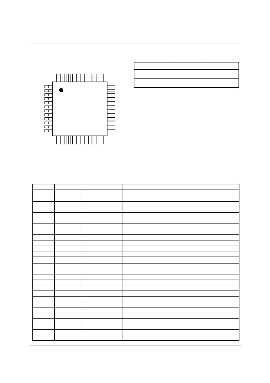
PIN CONFIGURATION
ORDERING INFORMATION
DEVICE
TEMP. RANGE
PACKAGE
WM2124CFT
0 to +70
o
C
48-pin TQFP
WM2124IFT
-40 to +85
o
C
48-pin TQFP
OE
B
D
VSS
SD
IO
DV
DD
SC
L
K
CLK
AVD
D
AP
AN
AVSS
AVD
D
ST
BY
37
47 46 45 44 43 42 41 40 39 38
48
DRV
S
S
DA
5
DA
1
DA
4
DA
3
DA
2
DA
0
DA
8
DRV
DD
DA
9
DA
7
DA
6
DRVDD
DB4
DB5
DB6
DB7
DB8
DB9
DB3
DB2
DB1
DB0
DRVSS
AVSS
REFB
REFT
CML
PWDNREF
BP
BN
COUTB
COUT
AVDD
AVSS
CSB
25
31
30
29
28
27
26
36
35
34
33
32
1
9
8
7
6
5
4
3
2
12
11
10
24
23
16 17 18 19 20 21 22
13 14 15
PIN DESCRIPTION
PIN
NAME
TYPE
DESCRIPTION
1
DRVDD
Supply
Positive digital output driver supply
2
DB9
Digital Output
Digital output for Q channel in dual bus mode bit 9 (msb)
3
DB8
Digital Output
Digital output for Q channel in dual bus mode bit 8
4
DB7
Digital Output
Digital output for Q channel in dual bus mode bit 7
5
DB6
Digital Output
Digital output for Q channel in dual bus mode bit 6
6
DB5
Digital Output
Digital output for Q channel in dual bus mode bit 5
7
DB4
Digital Output
Digital output for Q channel in dual bus mode bit 4
8
DB3
Digital Output
Digital output for Q channel in dual bus mode bit 3
9
DB2
Digital Output
Digital output for Q channel in dual bus mode bit 2
10
DB1
Digital Output
Digital output for Q channel in dual bus mode bit 1
11
DB0
Digital Output
Digital output for Q channel in dual bus mode bit 0 (lsb)
12
DRVSS
Ground
Negative digital output driver supply
13
DRVDD
Supply
Positive digital output driver supply
14
DA9
Digital Output
Digital output for I (dual bus mode), I/Q (single bus mode) bit 9 (msb)
15
DA8
Digital Output
Digital output for I (dual bus mode), I/Q (single bus mode) bit 8
16
DA7
Digital Output
Digital output for I (dual bus mode), I/Q (single bus mode) bit 7
17
DA6
Digital Output
Digital output for I (dual bus mode), I/Q (single bus mode) bit 6
18
DA5
Digital Output
Digital output for I (dual bus mode), I/Q (single bus mode) bit 5
19
DA4
Digital Output
Digital output for I (dual bus mode), I/Q (single bus mode) bit 4
20
DA3
Digital Output
Digital output for I (dual bus mode), I/Q (single bus mode) bit 3
21
DA2
Digital Output
Digital output for I (dual bus mode), I/Q (single bus mode) bit 2
22
DA1
Digital Output
Digital output for I (dual bus mode), I/Q (single bus mode) bit 1
23
DA0
Digital Output
Digital output for I (dual bus mode), I/Q (single bus mode) bit 0 (lsb)
24
DRVSS
Ground
Negative digital output driver supply
25
COUTB
Digital Output
Inverted latch clock output for digital outputs
26
COUT
Digital Output
Latch clock output for digital outputs
27
AVDD
Supply
Positive Analogue Supply

Advance Information
WM2124
w
w
w
w
AI Rev 1.2 January 2003
3
PIN
NAME
TYPE
DESCRIPTION
28
AVSS
Ground
Negative Analogue Supply
29
CSB
Digital Input
Serial interface chip select
30
REFB
Analogue Input/Output
ADC bottom reference
31
REFT
Analogue Input/Output
ADC top reference
32
CML
Analogue Output
ADC reference common mode level output
33
PWDNREF
Digital Input
Powerdown control for internal ADC reference generator
34
BP
Analogue Input
Positive input for the B signal channel
35
BN
Analogue Input
Negative input for the B signal channel
36
AVSS
Ground
Negative Analogue Supply
37
AVDD
Supply
Positive Analogue Supply
38
AP
Analogue Input
Positive input for the A signal channel
39
AM
Analogue Input
Negative input for the A signal channel
40
AVSS
Ground
Negative Analogue Supply
41
AVDD
Supply
Positive Analogue Supply
42
STBY
Digital Input
Standby control
43
DVSS
Ground
Negative Digital Supply
44
SDIO
Digital Input
Serial interface data input/output
45
DVDD
Supply
Positive Digital Supply
46
SCLK
Digital Input
Serial interface clock
47
CLK
Digital Input
Conversion clock. The input is sampled on each rising edge of CLK
when using a 40MHz input and alternate rising edges when using an
80MHz clock.
48
OEB
Digital Input
Output enable. A LOWon this terminal will enable the data output bus,
COUT and COUTB
ABSOLUTE MAXIMUM RATINGS
Absolute Maximum Ratings are stress ratings only. Permanent damage to the device may be caused by continuously operating at
or beyond these limits. Device functional operating limits and guaranteed performance specifications are given under Electrical
Characteristics at the test conditions specified.
ESD Sensitive Device. This device is manufactured on a CMOS process. It is therefore generically susceptible
to damage from excessive static voltages. Proper ESD precautions must be taken during handling and storage
of this device.
CONDITION
MIN
MAX
Digital supply voltage, DVDD to DVSS
-0.5V
+3.6V
Digital output driver supply voltage, DRVDD to DRVSS
-0.5V
+3.6V
Analogue supply voltage, AVDD to AVSS
-0.5V
+3.6V
Maximum ground difference between AVSS, DVSS and DRVSS
-0.5V
+0.5V
Voltage range digital inputs
DVSS � 0.5V
DVDD + 0.5V
Voltage range analogue inputs (includes CLK pin)
AVSS - 0.5V
AVDD + 0.5V
Operating temperature range, T
A
-45
�
C
+85
�
C
Storage temperature
-65
�
C
+150
�
C
Lead temperature (1.6mm from case for 10 seconds)
+300
�
C

WM2124
Advance Information
w
w
w
w
AI Rev 1.2 January 2003
4
RECOMMENDED OPERATINGCONDITIONS
PARAMETER
SYMBOL
TEST CONDITIONS
MIN
NOM
MAX
UNIT
Power Supply
Digital supply range
DVDD
3.0
3.3
3.6
V
Digital output driver supply range
DRVDD
3.0
3.3
3.6
V
Analogue supply range
AVDD
3.0
3.3
3.6
V
Ground
DVSS, DRVSS,
AVSS
0
V
Analogue and Reference Inputs
Reference Input Voltage (top)
VREFT
FCLK = 1MHz to 80MHz
1.9
2.0
2.15
V
Reference Input Voltage (bottom)
VREFB
FCLK = 1MHz to 80MHz
0.95
1.0
1.1
V
Reference Voltage Differential
VREFT-VREFB
FCLK = 1MHz to 80MHz
0.95
1.0
1.1
V
Reference Input Resistance
RREF
FCLK = 80MHz
1650
Reference Input Current
IREF
FCLK = 80MHz
0.62
mA
Analogue Input Voltage (differential)
VIN
V
Analogue Input Voltage (single
ended) Note 1
VIN
-1
1
V
Analogue Input Capacitance
CI
CML � 1.0
CML + 1.0
pF
Clock Input Note 2
8
V
Analogue Outputs
CML Voltage
AVDD/2
V
CML Output Resistance
2.3
k
Digital Inputs
High-Level Input Voltage
2.4
DVDD
V
Low-Level Input Voltage
DGND
0.8
V
Input Capacitance
5
pF
Clock Period
12.5
ns
Pulse Duration
Clock HIGH or LOW5.25
ns
Clock Period
25
ns
Pulse Duration
Clock HIGH or LOW11.25
ns
Notes
1.
Applies only when the signal reference input connects to CML.
2.
Clock pin is referenced to AVDD/AVSS.

Advance Information
WM2124
w
w
w
w
AI Rev 1.2 January 2003
5
ELECTRICAL CHARACTERISTICS
Test Conditions:
over recommended operation conditions with FCLK = 80MHz and use of internal voltage references, and PGA gain = 0dB,
unless otherwise stated.
PARAMETER
SYMBOL
TEST CONDITIONS
MIN
TYP
MAX
UNIT
DC Accuracy
Integral nonlinearity
INL
nternal References (Note 1)
-1.5
�
0.4
+1.5
LSB
Differential nonlinearity
DNL
nternal References (Note 2)
-0.9
�
0.4
+1.0
LSB
Zero error (Note 3)
0.12
% of FS
Full-Scale error
0.28
% of FS
Gain error
AVDD = DVDD = DRVDD =
3.3V
External References
(Note3)
0.24
% of FS
Missing codes
No missing codes guaranteed
References
REFT output voltage
V
REFTO
1.9
2.0
2.1
V
REFB output voltage
V
REFBO
Absolute Min/Max Values
Valid and Tested for AVDD
= 3.3V
0.95
1.0
1.05
V
Differential Reference Voltage
REFT-
RERB
0.95
1.0
1.05
V
Power Supplies
AVDD
64
72
DVDD
1.7
2.2
IDD Operating Supply Current
DRVDD
AVDD = DVDD = DRVDD =
3.3V, CL = 10pF, VIN =
3.5MHz, -1dBFS
18
27
mA
PWDN_REF = L
275
345
Power Dissipation
PD
PWDN_REF = H
240
300
mW
Standby Power
PD(STBY)
STDBY = H, CLK held
HIGH or LOW
95
150
uW
Power-Up Time for all
references from Standby
tPD
550
ms
Wake up Time
tWU
External Reference
40
us
Digital Inputs
High-Level Input Current on
Digital Inputs incl. CLK
I
IH
-1
+1
uA
Low-Level Input Current on
Digital Inputs incl. CLK
I
IL
AVDD = DVDD = DRVDD =
3.6V
-1
+1
uA
Digital Outputs
High-Level Output Voltage
V
OH
AVDD = DVDD = DRVDD =
3.0V at I
OH
= 50uA, Digital
Outputs Forced HIGH
2.8
2.96
V
Low-Level Output Voltage
V
OL
AVDD = DVDD = DRVDD =
3.0V at I
OH
= 50uA, Digital
Outputs Forced LOW
0.04
0.2
V
Output Capacitance
C
O
5
pF
High-Impedance State Output
Current to High-Level
I
OZH
-1
+1
uA
High-Impedance State Output
Current to Low-Level
I
OZL
AVDD = DVDD = DRVDD =
3.6V
-1
+1
uA
C
LOAD
= 10pF, Single-Bus
Mode
3
ns
Data Output Rise and Fall Time
C
LOAD
= 10pF, Dual-Bus
Mode
5
ns
Notes
1.
INL refers to the deviation of each individual code from a line drawn from zero to full-scale. The point used as zero
occurs 1/2LSB before the first code transition. The full-scale point is defined as a level 1/2LSB beyond the last code
transition. The deviation is measured from the center of each particular code to the best fit line between these two
points.