WM2130
10-bit 30MSPS Analogue-To-Digital Converter
Production Data, April 2001, Rev 1.2
WOLFSON MICROELECTRONICS LTD
Lutton Court, Bernard Terrace, Edinburgh, EH8 9NX, UK
Tel: +44 (0) 131 667 9386
Fax: +44 (0) 131 667 5176
Email: sales@wolfson.co.uk
www.wolfsonmicro.com
Production Data datasheets contain final
specifications current on publication date.
Supply of products conforms to Wolfson
Microelectronics' Terms and Conditions.
2001 Wolfson Microelectronics Ltd.
DESCRIPTION
The WM2130 is a high speed 10-bit analogue-to-digital
converter and operates with independent analogue and
digital supplies of 3V to 5.5V. This device includes a high
bandwidth sample and hold and internal voltage references.
Conversion is controlled by a single clock input.
The differential-input sample and hold input gives excellent
common-mode noise immunity and low distortion. The
device can also be driven in a single ended fashion.
The device provides internal reference voltages for setting
the ADC full-scale range without the requirement for
external circuitry. The WM2130 can also accept external
reference levels for applications where higher precision
references are required.
The WM2130 has also been designed to offer a speed
upgrade to users of the AD876 and a replacement for the
AD9200 and AD9202 devices. The WM2130 operates as
an AD876 in those design slots but at speeds of up to 50%
faster.
FEATURES
�
10-bit resolution ADC
�
30MSPS conversion rate
�
Wide input bandwidth (150 MHz full-power bandwidth)
sample and hold input amplifier
�
Independent analogue and digital supplies
�
Adjustable internal voltage references
�
Out of range indicator
�
Low power: 87mW typical at 3V supplies
�
Powerdown mode to 3mW typical
�
28-pin TSSOP package
APPLICATIONS
�
Set Top Box (STB)
�
IF and Baseband Digitisation
�
Medical
Imaging
�
High speed data acquisition
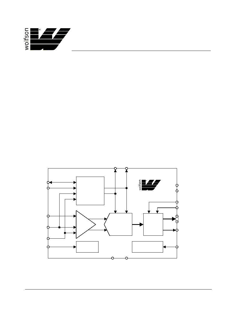
BLOCK DIAGRAM
WM2130
AIN
PRECISION
REFERENCE
CIRCUITS
+
SHA
-
REFTS
D[9:0]
REFBF
REFTF
OVR
REFBS
OEB
MODE
REFSENSE
POWER-DOWN
CONTROL
STBY
AGND
AVDD
DGND
DVDD
M876B
TIMING
CONTROL
CLK
OUTPUT
BUFFERS
ADC
WM2130
Production Data
WOLFSON MICROELECTRONICS LTD
PD Rev 1.2 April 2001
2
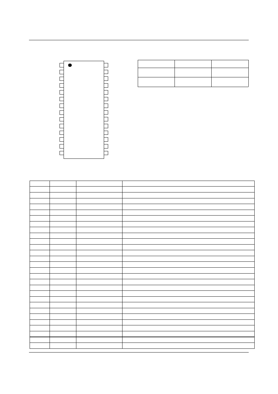
PIN CONFIGURATION
ORDERING INFORMATION
DEVICE
TEMP. RANGE
PACKAGE
WM2130CDT/V
0 to +70
o
C
28-pin TSSOP
WM2130IDT/V
-40 to +85
o
C
28-pin TSSOP
16
15
14
20
19
18
17
5
6
7
1
2
3
4
13
12
11
8
9
10
DIO0
OVR
OEB
AGND
DVDD
REFTS
REFBS
REFBF
REFTF
MODE
VREF
AIN
AVDD
DIO8
REFSENSE
DIO2
DIO3
DIO1
DIO7
AGND
DIO6
DIO5
M876B
DIO4
21
22
23
24
25
26
27
28
DIO9
DGND
STBY
CLK
PIN DESCRIPTION
PIN
NAME
TYPE
DESCRIPTION
1
AGND
Ground
Analogue Ground
2
DVDD
Supply
Positive Digital Supply
3
DO0
Digital Output
Digital output bit 0 (lsb)
4
DO1
Digital Output
Digital output bit 1
5
DO2
Digital Output
Digital output bit 2
6
DO3
Digital Output
Digital output bit 3
7
DO4
Digital Output
Digital output bit 4
8
DO5
Digital Output
Digital output bit 5
9
DO6
Digital Output
Digital output bit 6
10
DO7
Digital Output
Digital output bit 7
11
DO8
Digital Output
Digital output bit 8
12
DO9
Digital Output
Digital output bit 9 (msb)
13
OVR
Digital Output
Over-range output (tri-statable)
14
DGND
Ground
Digital Ground
15
CLK
Digital Input
Clock input
16
STBY
Digital Input
Powerdown control
17
OEB
Digital Input
Output enable bar � low to enable DO[9:0] and OVR
18
REFSENSE
Analogue Input/Output
VREF mode control
19
AGND
Ground
Negative Analogue Supply
20
M876B
Digital Input
AD876 mode select
21
REFTS
Analogue Input
Top reference sense
22
REFTF
Analogue Input/Output
Top reference force
23
MODE
Digital Input
Input mode select
24
REFBF
Analogue Input/Output
Bottom reference force
25
REFBS
Analogue Input
Bottom reference sense
26
VREF
Analogue Input/Output
Internal reference output
27
AIN
Analogue Input
Analog Input
28
AVDD
Supply
Positive Analogue Supply
Production Data
WM2130
WOLFSON MICROELECTRONICS LTD
PD Rev 1.2 April 2001
3
ABSOLUTE MAXIMUM RATINGS
Absolute Maximum Ratings are stress ratings only. Permanent damage to the device may be caused by continuously operating at
or beyond these limits. Device functional operating limits and guaranteed performance specifications are given under Electrical
Characteristics at the test conditions specified.
ESD Sensitive Device. This device is manufactured on a CMOS process. It is therefore generically susceptible
to damage from excessive static voltages. Proper ESD precautions must be taken during handling and storage
of this device.
As per specifications IPC/JEDEC J-STD-020A and JEDEC A113-B, this product requires specific storage conditions prior to
surface mount assembly. It has been classified as having a Moisture Sensitivity Level of 2 and as such will be supplied in
vacuum-sealed moisture barrier bags.
CONDITION
MIN
MAX
Digital supply voltage, DVDD to DGND
-0.3V
+6.5V
Analogue supply voltage, AVDD to AGND
-0.3V
+6.5V
Supply voltage difference, AVDD to DVDD
-6.5V
+6.5V
Ground difference, AGND to DGND
-0.3V
+0.3V
Digital inputs voltage range (DO[9:0], STBY, OEB, M876B)
DGND - 0.3V
DVDD + 0.3V
Voltage range analogue inputs (REFTS, REFBS, REFTF, REFBF, AIN,
VREF, REFSENSE, CLK, MODE)
AGND - 0.3V
AVDD + 0.3V
Storage temperature
-65
�
C
+150
�
C
Soldering lead temperature, 1.6mm (1/16 inch) from package body for
10 seconds
+300
�
C
RECOMMENDED OPERATING CONDITIONS
PARAMETER
SYMBOL
TEST CONDITIONS
MIN
NOM
MAX
UNIT
Digital supply range
DVDD
3.0
3.3
5.5
V
Analogue supply range
AVDD
3.0
3.3
5.5
V
Clock frequency
f
CLK
5
30
MHz
Clock duty cycle
45
50
55
%
WM2130C
0
�
C
Operating Free Air Minimum
Temperature
T
MIN
WM2130I
-40
�
C
WM2130C
70
�
C
Operating Free Air Maximum
Temperature
T
MAX
WM2130I
85
�
C
WM2130
Production Data
WOLFSON MICROELECTRONICS LTD
PD Rev 1.2 April 2001
4
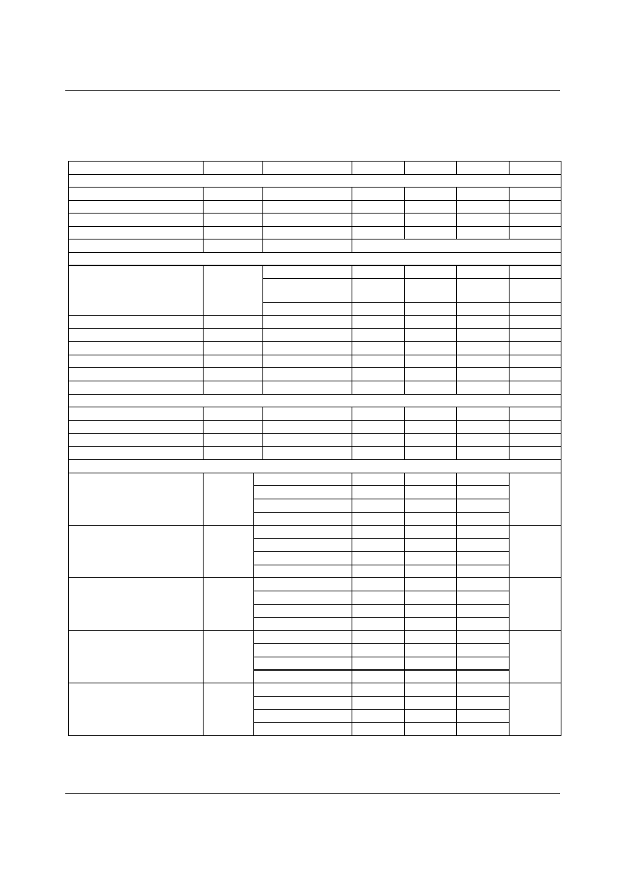
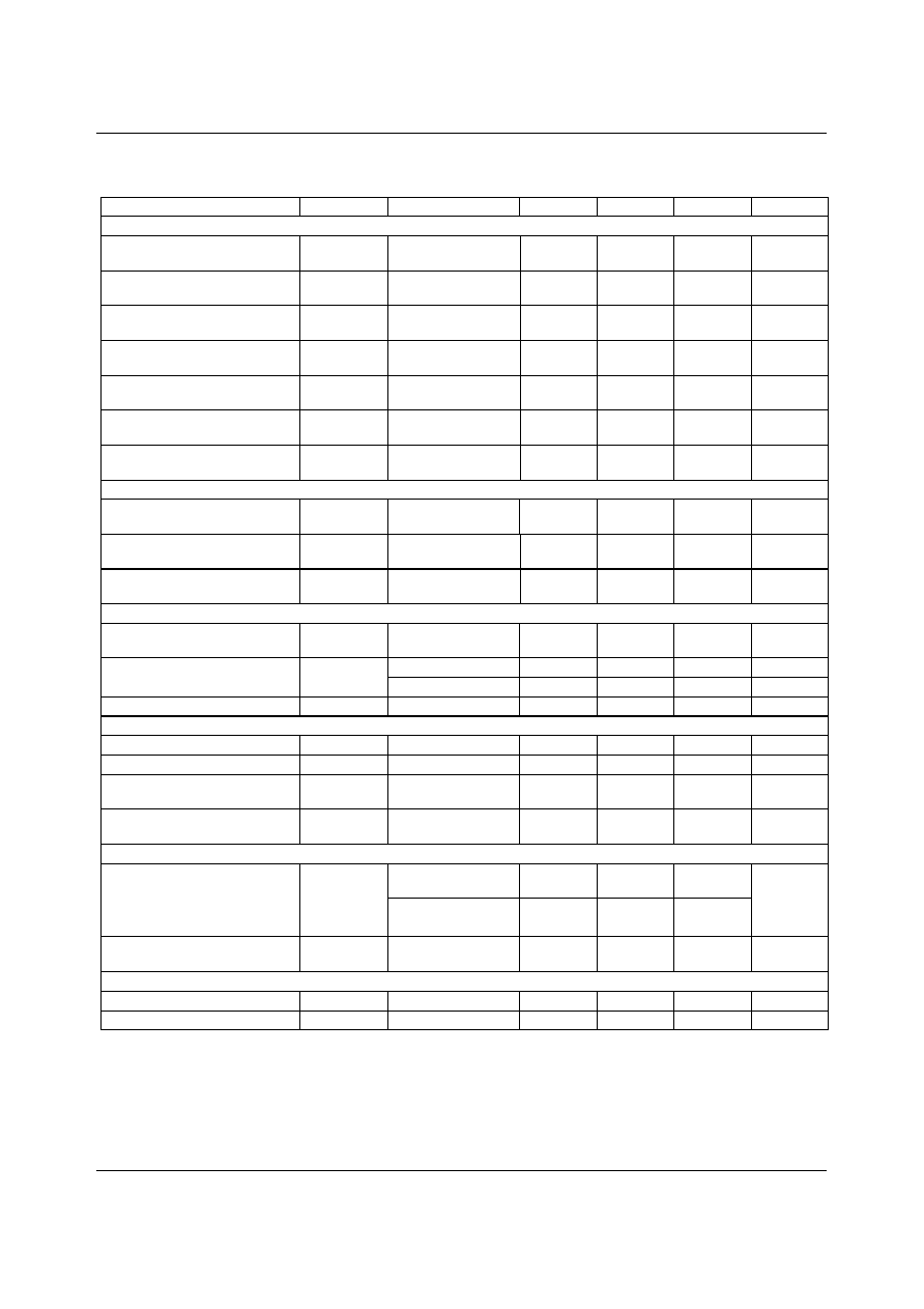
ELECTRICAL CHARACTERISTICS
Test Conditions:
AVDD = DVDD = 3.0V, f
CLK
= 30MHz, 50% Duty cycle, MODE = AVDD, REFTS = 2.5V, REFBS = 0.5V, T
A
= T
MIN
to T
MAX
,
unless otherwise stated.
PARAMETER
SYMBOL
TEST CONDITIONS
MIN
TYP
MAX
UNIT
DC Accuracy
Integral nonlinearity
INL
�
1.0
�
2.0
LSB
Differential nonlinearity
DNL
�
0.3
�
1.0
LSB
Offset error
0.4
2.0
% of FS
Gain error
1.4
3.5
% of FS
Missing codes
No missing codes guaranteed
Analogue Input Signal to AIN pin
MODE = AGND
REFBS
REFTS
V
MODE = AVDD / 2,
V
CMCS
fixed
V
CMCS
�
VREF/2
V
CMCS
+
VREF/2
V
Input signal range
MODE = AVDD
REFBS
REFTS
V
AIN voltage limits
AGND
AVDD
V
Switched input capacitance
1.2
pF
Analogue input bandwidth
150
MHz
DC leakage current
�
Full-scale input
�
60
�
A
Aperture delay
t
A
4
ns
Aperture jitter
2
ps rms
Conversion Characteristics
Conversion frequency
f
CLK
5
30
MHz
Pipeline delay
3
CLK cycles
Aperture delay
t
A
4
ns
Aperture jitter
2
ps rms
Dynamic Performance
f
IN
= 3.5MHz
8.4
9
f
IN
=3.5MHz, AVDD 5V
9
f
IN
= 15MHz
7.8
Effective number of bits
ENOB
f
IN
=15MHz, AVDD 5V
7.7
dB
f
IN
= 3.5MHz
56
60.6
f
IN
=3.5MHz, AVDD 5V
64.6
f
IN
= 15MHz
48.5
Spurious free dynamic range
SFDR
f
IN
=15MHz, AVDD 5V
53
dB
f
IN
= 3.5MHz
-60
-56
f
IN
=3.5MHz, AVDD 5V
-66.9
f
IN
= 15MHz
-47.5
Total Harmonic Distortion
THD
f
IN
=15MHz, AVDD 5V
-53.1
dB
f
IN
= 3.5MHz
53
57
f
IN
=3.5MHz, AVDD 5V
56
f
IN
= 15MHz
53.1
Signal to noise ratio
SNR
f
IN
=15MHz, AVDD 5V
49.4
dB
f
IN
= 3.5MHz
52.5
56
f
IN
=3.5MHz, AVDD 5V
56
f
IN
= 15MHz
48.6
Signal to noise and distortion
ratio
SINAD
f
IN
=15MHz, AVDD 5V
48.1
dB
Production Data
WM2130
WOLFSON MICROELECTRONICS LTD
PD Rev 1.2 April 2001
5
Test Conditions:
AVDD = DVDD = 3.0V, f
CLK
= 30MHz, 50% Duty cycle, MODE = AVDD, REFTS = 2.5V, REFBS = 0.5V, T
A
= T
MIN
to T
MAX
,
unless otherwise stated.
PARAMETER
SYMBOL
TEST CONDITIONS
MIN
TYP
MAX
UNIT
Analogue Reference Inputs / Outputs in Top/Bottom Mode (MODE=AVDD)
Bottom reference voltage
applied to REFBS
0
AVDD � 1
V
Top reference voltage applied to
REFTS
1
AVDD
V
Differential reference input
(REFTS � REFBS)
V
TB
1
2
V
Switched input capacitance on
REFBS
0.6
pF
Switched input capacitance on
REFTS
0.6
pF
REFBF output voltage
(AVDD -
V
TB
)/2
V
REFTF output voltage
(AVDD +
V
TB
)/2
V
Analogue Reference Inputs / Outputs in Centre-Span Mode (MODE=AVDD/2)
Reference voltage derived or
applied to VREF
1
2
V
REFBF output voltage
(AVDD -
VREF)/2
V
REFTF output voltage
(AVDD +
VREF)/2
V
Analogue Reference Inputs / Outputs in Full External Reference Mode (MODE=AGND) (Note 1)
Differential reference voltage
applied (REFTF � REFBF)
1
2
V
AVDD = 3.0V
1.3
1.5
1.7
V
Reference input common mode
(REFTF + REFBF) / 2
AVDD = 5.0V
2.0
2.5
3.0
V
Reference input resistance
680
VREF Input / Output specifications
Internal 1V reference to VREF
REFSENSE = VREF
0.95
1.0
1.05
V
Internal 2V reference to VREF
REFSENSE = AGND
1.9
2.0
2.1
V
External reference applied to
VREF pin in centre-span mode
REFSENSE = AVDD,
MODE = AVDD / 2
1
2
V
Input impedance in centre-span
mode
REFSENSE = AVDD,
MODE = AVDD / 2
18
k
Power Supplies
AVDD = DVDD = 3V,
MODE = AGND
29
40
Operating supply current
I
AVDD
+ I
DVDD
AVDD = DVDD = 5V
50
mA
Standby Power
P
STBY
AVDD = DVDD = 3V,
MODE = AGND
3
5
mW
Digital Logic Levels (CMOS Levels)
Input LOW level
V
IL
(Note 2)
0.2 x VDD
V
Input HIGH level
V
IH
(Note 2)
0.8 x VDD
V
Notes
1.
In full external reference mode the REFTF and REFTS pins should be shorted together, and the REFBF and REFBS
pins should be shorted together. Please refer to device operation examples in the device description section of the
datasheet.
2.
Digital input and output levels refer to the supply used for the input/output buffer on the relevant pin. MODE refers to
the AVDD supply, all other digital input/output refers to the DVDD supply.