 | –≠–ª–µ–∫—Ç—Ä–æ–Ω–Ω—ã–π –∫–æ–º–ø–æ–Ω–µ–Ω—Ç: WM2152IDT | –°–∫–∞—á–∞—Ç—å:  PDF PDF  ZIP ZIP |
Document Outline
- WM2152
- 12-bit, 30MSPS ADC
- Product Preview, March 2001, Rev 1.1
- DESCRIPTION
- FEATURES
- APPLICATIONS
- BLOCK DIAGRAM
- PIN CONFIGURATION
- ORDERING INFORMATION
- PIN DESCRIPTION
- ABSOLUTE MAXIMUM RATINGS
- ELECTRICAL CHARACTERISTICS
- TYPICAL SYSTEM PERFORMANCE
- PACKAGE DIMENSIONS
WM2152
12-bit, 30MSPS ADC
Product Preview, March 2001, Rev 1.1
WOLFSON MICROELECTRONICS LTD
Lutton Court, Bernard Terrace, Edinburgh, EH8 9NX, UK
Tel: +44 (0) 131 667 9386
Fax: +44 (0) 131 667 5176
Email: sales@wolfson.co.uk
www.wolfsonmicro.com
Product Preview data sheets contain
specifications for products in the formative
phase of development. These products may
be changed or discontinued without notice.
2001 Wolfson Microelectronics Ltd
.
DESCRIPTION
The WM2152 is a high speed 12-bit analogue-to-digital
converter operating on a 3.3V supply. This device includes
a high bandwidth sample and hold and internal voltage
references. Conversion is controlled by a single clock input.
The device has a differential sample and hold input which
gives excellent common-mode noise immunity and low
distortion. The maximum differential input voltage can be
set by the user, via two mode selection pins, to be 1V or 2V.
A third PGA mode is designed particularly for single-ended
input signals such as composite video sources. Single-
ended input signals require one side of the differential input
to be tied to an external voltage source.
The device provides internal reference voltages for setting
the ADC full-scale range without the requirement for
external circuitry. The WM2152 can also accept external
reference levels for applications where common or high
precision references are required.
The WM2152 provides an out of range indicator flag to
indicate when the input signal exceeds the converter's full
scale range. An output enable pin allows several devices to
share a common bus. Power down mode for the device is
under the control of the two mode control pins and takes
power consumption down to less than 36
µ
W.
FEATURES
∑
12-bit resolution ADC
∑
30MSPS conversion rate
∑
Programmable Gain Amplifier (PGA)
∑
Out of range indicator
∑
Low power - 160mW typical at 3.3V supplies
∑
Powerdown mode to 30
µ
W typical
∑
66dB SNR for 3.58MHz input signal
∑
-78db THD for 3.58MHz input signal
∑
28-pin TSSOP package
APPLICATIONS
∑
Direct IF sampling
∑
Baseband
digitisation
∑
Video
Digitisation
∑
Portable
instrumentation
∑
Digital
imaging
∑
High speed data acquisition
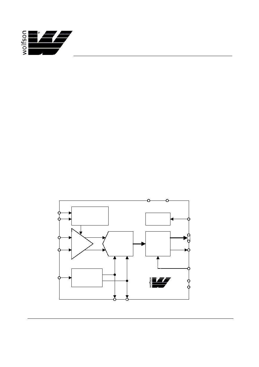
BLOCK DIAGRAM
VINP (5)
PRECISION
REFERENCE
CIRCUITS
ADC
+
PGA
-
VINM (6)
D[11:0]
(12-18, 21-25)
OUTPUT
BUFFERS
(11) OVRNG
AVDD
(8, 27)
(9)
VRT
(10)
VRB
(26) OEB
(19) DGND
(20) DVDD
TIMING
CONTROL
(28) CLK
CONFIGURATION
CONTROL CIRCUIT
CON0 (3)
CON1 (2)
EXTREF (4)
AVDD
(1,7)
WM2152

WM2152
Product Preview
WOLFSON MICROELECTRONICS LTD
PP Rev 1.1 March 2001
2
PIN CONFIGURATION
ORDERING INFORMATION
DEVICE
TEMP. RANGE
PACKAGE
XWM2152CDT
0 to +70
o
C
28-pin TSSOP
XWM2152IDT
-40 to +85
o
C
28-pin TSSOP
16
15
14
20
19
18
17
5
6
7
1
2
3
4
13
12
11
8
9
10
CON0
D10
D7
AGND
CON1
D4
D0
D1
D3
D2
OEB
AVDD
CLK
OVRNG
D5
VINP
VINM
EXTREF
VRB
DGND
VRT
AVDD
DVDD
AGND
21
22
23
24
25
26
27
28
D11
D9
D6
D8
PIN DESCRIPTION
PIN
NAME
TYPE
DESCRIPTION
1
AGND
Supply
Analogue Ground (for Timing Circuitry)
2
CON1
Digital Input
Mode control pin 1
3
CON0
Digital Input
Mode control pin 0
4
EXTREF
Digital Input
Reference select pin
5
VINP
Analogue Input
Positive analogue input
6
VINM
Analogue Input
Negative analogue input
7
AGND
Supply
Analogue ground
8
AVDD
Supply
Analogue power supply
9
VRT
Analogue I/O
Upper ADC reference voltage
10
VRB
Analogue I/O
Lower ADC reference voltage
11
OVRNG
Digital Output
Out of range indicator
12
D11
Digital Output
Data output bit 11 (MSB)
13
D10
Digital Output
Data output bit 10
14
D9
Digital Output
Data output bit 9
15
D8
Digital Output
Data output bit 8
16
D7
Digital Output
Data output bit 7
17
D6
Digital Output
Data output bit 6
18
D5
Digital Output
Data output bit 5
19
DGND
Supply
Digital ground
20
DVDD
Supply
Digital power supply
21
D4
Digital Output
Data output bit 4
22
D3
Digital Output
Data output bit 3
23
D2
Digital Output
Data output bit 2
24
D1
Digital Output
Data output bit 1
25
D0
Digital Output
Data output bit 0 (LSB)
26
OEB
Digital Input
Output enable (low = enable, high = disable)
27
AVDD
Supply
Analogue Power Supply (for Timing Circuitry)
28
CLK
Digital Input
ADC conversion clock

Product Preview
WM2152
WOLFSON MICROELECTRONICS LTD
PP Rev 1.1 March 2001
3
ABSOLUTE MAXIMUM RATINGS
Absolute Maximum Ratings are stress ratings only. Permanent damage to the device may be caused by continuously operating at
or beyond these limits. Device functional operating limits and guaranteed performance specifications are given under Electrical
Characteristics at the test conditions specified.
ESD Sensitive Device. This device is manufactured on a CMOS process. It is therefore generically susceptible
to damage from excessive static voltages. Proper ESD precautions must be taken during handling and storage
of this device.
CONDITION
MIN
MAX
Digital supply voltage, DVDD to DGND
-0.3V
+4.0V
Input clock supply voltage, CLKVDD to CLKGND
-0.3V
+4.0V
Analogue supply voltage, AVDD to AGND
-0.3V
+4.0V
Maximum ground difference between AGND, DGND and CLKGND
-0.3V
+0.3V
Voltage range digital inputs
DGND - 0.3V
DVDD + 0.3V
Voltage range analogue inputs
AGND - 0.3V
AVDD + 0.3V
Voltage range CLK input
CLKGND - 0.3V
CLKVDD + 0.3V
Operating junction temperature range, T
J
-40
∞
C
+150
∞
C
Storage temperature
-65
∞
C
+150
∞
C
Lead temperature (1.6mm from package body for 10 seconds)
+300
∞
C
WM2152
Product Preview
WOLFSON MICROELECTRONICS LTD
PP Rev 1.1 March 2001
4
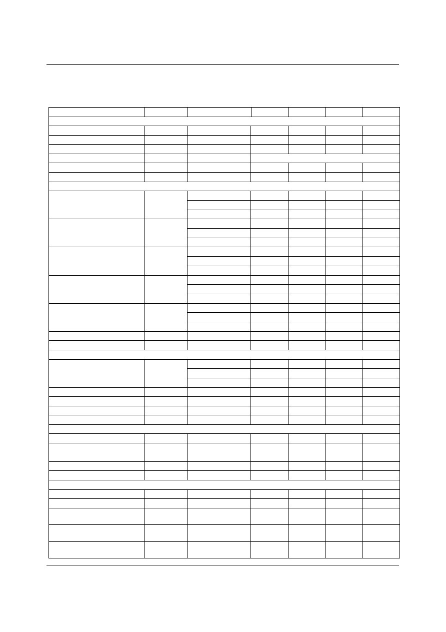
ELECTRICAL CHARACTERISTICS
Test Conditions:
AVDD = DVDD = 3.3V, f
CLK
= 30MHz, EXTREF = AGND, Mode=1, T
A
= T
MIN
to T
MAX
, unless otherwise stated.
PARAMETER
SYMBOL
TEST CONDITIONS
MIN
TYP
MAX
UNIT
DC Characteristics
Resolution
12
bits
Integral Nonlinearity
INL
All modes
-2.5
±
1.2
+2
LSB
Differential Nonlinearity
DNL
All modes
±
0.4
±
1
LSB
Missing Codes
All modes
No missing codes guaranteed
Offset Error
All modes
0.5
1.2
%FSR
Gain Error
All modes
0.5
3.5
%FSR
Dynamic Performance (Note 1)
f
IN
=3.58MHz
10.9
bits
f
IN
=10MHz
10.6
10.9
bits
Effective number of bits
ENOB
f
IN
=15MHz
10.8
bits
f
IN
=3.58MHz
-76
dB
f
IN
=10MHz
-74
-65
dB
Total harmonic distortion
THD
f
IN
=15MHz
-72.5
dB
f
IN
=3.58MHz
68
dB
f
IN
=10MHz
66
68
dB
SNR
f
IN
=15MHz
67.7
dB
f
IN
=3.58MHz
67.4
dB
f
IN
=10MHz
65.6
67.4
dB
Signal to noise and distortion
ratio
SINAD
f
IN
=15MHz
66.6
dB
f
IN
=3.58MHz
78.1
dB
f
IN
=10MHz
67
76.4
dB
Spurious free dynamic range
SFDR
f
IN
=15MHz
74.6
dB
Differential phase
DP
0.12
deg
Differential gain
DG
0.01
%
Analogue Input Signal to (VINP ≠ VINM)
Mode=1, VREF = 1V
-0.5
0.5
V
Mode=2, VREF = 1V
-1
1
V
Input Span
Mode=3, VREF = 1V
0
1
V
Input (VINP or VINM) range
All modes
0
AVDD
V
Input capacitance
C
IN
All modes
6
pF
Analogue input bandwidth
180
MHz
Power supply rejection ratio
PSRR
54
dB
Conversion Characteristics
Conversion frequency
f
CLK
5
30
MHz
Pipeline delay
5
cycles of
CLK
Aperture delay
t
A
2.0
ns
Aperture jitter
2.0
ps rms
Internal Voltage References (Note 3)
Upper reference voltage
VRT
2.15
V
Lower reference voltage
VRB
1.15
V
Differential reference voltage
(VRT-VRB)
VREF
0.95
1
1.05
V
Differential reference voltage
(VRT-VRB) accuracy
-5
+5
%
Power up time of references
from standby
t
PU
100
µ
s

Product Preview
WM2152
WOLFSON MICROELECTRONICS LTD
PP Rev 1.1 March 2001
5
Test Conditions:
AVDD = DVDD = 3.3V, f
CLK
= 30MHz, EXTREF = AGND, Mode=1, T
A
= T
MIN
to T
MAX
, unless otherwise stated.
PARAMETER
SYMBOL
TEST CONDITIONS
MIN
TYP
MAX
UNIT
External Voltage References
Externally applied VRT
reference range
2
2.5
V
Externally applied VRB
reference range
1.05
1.3
V
Externally applied differential
reference range (VRT-VRB)
0.75
1.05
V
Reference Input Resistance
(VRT to VRB)
9
k
Digital Inputs / Outputs
Input LOW level
V
IL
0.2 x VDD
V
Input HIGH level
V
IH
0.8 x VDD
V
High level output voltage
V
OL
I
OH
=50
µ
A
DVDD-0.4
V
Low level output voltage
V
OH
I
OL
=-50
µ
A
0.4
V
High Impedance Output Current
±
1
µ
A
Rise/Fall time
C
LOAD
=10pF
5.5
ns
Power Supplies
CLKVDD supply current
I
AA1
f
CLK
= 30MHz
3.0
3.3
3.6
mA
AVDD supply current
I
AA2
35
mA
DVDD supply current
I
DD
10
mA
Total supply current
I
TOT
f
CLK
= 30MHz
48.3
mA
Total supply current in standby
mode
I
SB
f
CLK
= 0MHz
10
µ
A
Power consumption
f
CLK
= 30MHz
168
220
mW
Notes
1.
Input amplitudes for all single tone dynamic tests are all -0.5dBFS.
2.
Inputs for two-tone IMD are 4.4MHz and 4.5MHz, each at -7dBFS.
3.
The internal reference voltage is not intended for use driving off-chip.