 | –≠–ª–µ–∫—Ç—Ä–æ–Ω–Ω—ã–π –∫–æ–º–ø–æ–Ω–µ–Ω—Ç: WM2631IDT | –°–∫–∞—á–∞—Ç—å:  PDF PDF  ZIP ZIP |
Document Outline
- WM2631
- Octal 10-bit, Serial Input, Voltage Output DAC with Internal Reference
- Production Data, April 2001, Rev 1.1
- FEATURES
- DESCRIPTION
- APPLICATIONS
- ORDERING INFORMATION
- BLOCK DIAGRAM
- TYPICAL PERFORMANCE
- PIN CONFIGURATION
- PIN DESCRIPTION
- ABSOLUTE MAXIMUM RATINGS
- RECOMMENDED OPERATING CONDITIONS
- ELECTRICAL CHARACTERISTICS
- SERIAL INTERFACE
- TYPICAL PERFORMANCE GRAPHS
- DEVICE DESCRIPTION
- GENERAL FUNCTION
- SERIAL INTERFACE
- SOFTWARE CONFIGURATION OPTIONS
- APPLICATIONS INFORMATION
- LINEARITY, OFFSET, AND GAIN ERROR
- POWER SUPPLY DECOUPLING AND GROUNDING
- PACKAGE DIMENSIONS

WM2631
Octal 10-bit, Serial Input, Voltage Output DAC
with Internal Reference
Production Data, April 2001, Rev 1.1
WOLFSON MICROELECTRONICS LTD
Bernard Terrace, Edinburgh, EH8 9NX, UK
Tel: +44 (0) 131 667 9386
Fax: +44 (0) 131 667 5176
Email: sales@wolfson.co.uk
www.wolfsonmicro.com
Production Data datasheets contain final
specifications current on publication date.
Supply of products conforms to Wolfson
Microelectronics' Terms and Conditions.
2001 Wolfson Microelectronics Ltd
.
FEATURES
∑
Eight 10-bit DACs in one package
∑
Dual supply 2.7V to 5.5V operation
∑
DNL
±
0.1 LSBs, INL
±
0.5 LSBs typical
∑
Programmable settling time / power
(1.0
µ
s typical in fast mode)
∑
Internal programmable voltage reference
∑
Microcontroller compatible serial interface
∑
Power down mode ( < 0.1
µ
A)
∑
Monotonic over temperature
∑
Data output for daisy chaining
APPLICATIONS
∑
Battery powered test instruments
∑
Digital offset and gain adjustment
∑
Battery operated / remote industrial controls
∑
Programmable loop controllers
∑
CNC machine tools
∑
Machine and motion control devices
∑
Wireless telephone and communication systems
∑
Robotics
ORDERING INFORMATION
DEVICE
TEMP. RANGE
PACKAGE
WM2631CDT
0
∞
to 70
∞
C
20-pin TSSOP
WM2631IDT
-40
∞
to 85
∞
C
20-pin TSSOP
DESCRIPTION
The WM2631 is an octal, 10-bit, resistor string digital-to-
analogue converter. The eight individual DACs contained in
the IC can be switched in pairs between fast and slow (low
power) operation modes, or powered down, under software
control. Alternatively, the whole device can be powered
down, reducing current consumption to less than 0.1
µ
A.
The DAC outputs are buffered by a rail-to-rail amplifier with
a gain of two, which is configurable as Class A (fast mode)
or Class AB (for low-power mode).
The WM2631 has been designed to interface directly to
industry standard microprocessors and DSPs, and can
operate on two separate analogue and digital power
supplies. It is programmed with a 16-bit serial word
comprising 4 address bits and up to 12 DAC or control
register data bits. All eight DACs can be simultaneously
forced to a preset value using a preset input pin.
A daisy-chain data output makes it possible to control
several of Wolfson's octal DACs from the same interface,
without increasing the number of control lines.
The device is available in a 20-pin TSSOP package.
Commercial temperature (0∞ to 70∞C) and Industrial
temperature (-40∞ to 85∞C) variants are supported.
BLOCK DIAGRAM
TYPICAL PERFORMANCE
LATCH
POWER/SPEED
CONTROL
RESISTOR
STRING
(12) OUT A
DAC A
DIN (2)
SCLK (3)
FS (4)
PREB (5)
1.024V / 2.048V
SELECTABLE
REFERENCE
DOUT (19)
REF
(16)
DACs B, C, D, E, F, G, H
as DAC A
(6-9, 13-15)
OUT B to H
REF
SERIAL
INTERFACE
AND
CONTROL
LOGIC
MODE (17)
AVDD
(11)
DVDD
(20)
AGND
(10)
DGND
(1)
LOADB
(18)
-0.2
-0.15
-0.1
-0.05
0
0.05
0.1
0.15
0.2
0
128
256
384
512
640
768
896
1024
DIGITAL CODE
D
i
f
f
e
r
e
nt
ia
l N
on-
Line
a
r
it
y
(
L
SB
s
)
WM2631
Production Data
WOLFSON MICROELECTRONICS LTD
PD Rev 1.1 April 2001
2
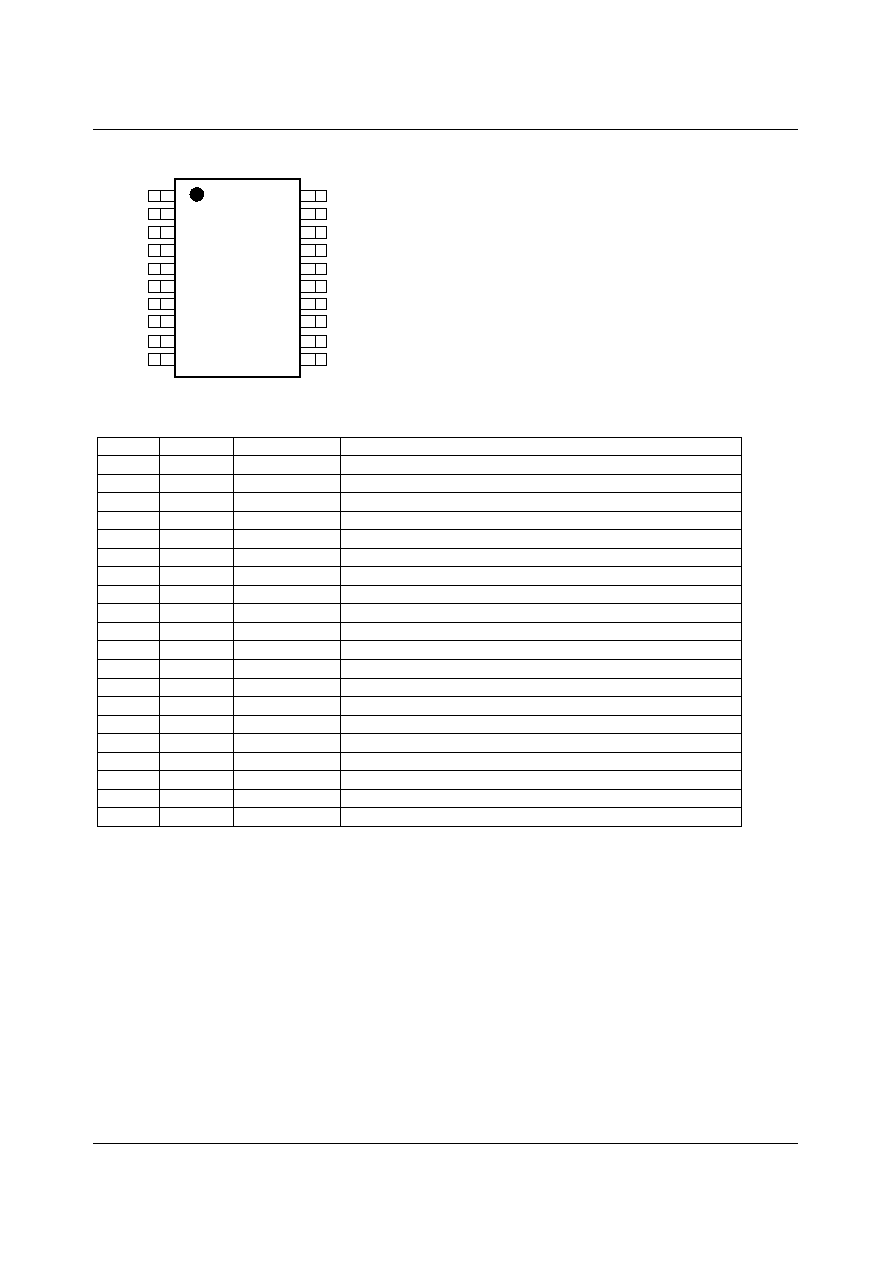
PIN CONFIGURATION
9
10
OUTH
AGND
12
11
OUTA
AVDD
20
13
14
15
16
17
18
19
DVDD
OUTC
OUTD
REF
MODE
LOADB
DOUT
OUTB
8
1
2
3
4
5
6
7
OUTG
DIN
SCLK
FS
PREB
OUTE
OUTF
DGND
PIN DESCRIPTION
PIN NO
NAME
TYPE
DESCRIPTION
1
DGND
Supply
Digital Ground
2
DIN
Digital input
Digital serial data input
3
SCLK
Digital input
Serial clock input
4
FS
Digital input
Frame sync input
5
PREB
Digital input
Preset input
6
OUTE
Analogue output
DAC Output E
7
OUTF
Analogue output
DAC Output F
8
OUTG
Analogue output
DAC Output G
9
OUTH
Analogue output
DAC Output H
10
AGND
Supply
Analogue Ground
11
AVDD
Supply
Analogue positive power supply
12
OUTA
Analogue output
DAC Output A
13
OUTB
Analogue output
DAC Output B
14
OUTC
Analogue output
DAC Output C
15
OUTD
Analogue output
DAC Output D
16
REF
Analogue I/O
Voltage reference input / output
17
MODE
Digital input
Input mode
18
LOADB
Digital input
Load DAC
19
DOUT
Digital output
Serial data output
20
DVDD
Supply
Digital positive power supply
Production Data
WM2631
WOLFSON MICROELECTRONICS LTD
PD Rev 1.1 April 2001
3
ABSOLUTE MAXIMUM RATINGS
Absolute Maximum Ratings are stress ratings only. Permanent damage to the device may be caused by continuously operating at
or beyond these limits. Device functional operating limits and guaranteed performance specifications are given under Electrical
Characteristics at the test conditions specified.
ESD Sensitive Device. This device is manufactured on a CMOS process. It is therefore generically susceptible
to damage from excessive static voltages. Proper ESD precautions must be taken during handling and storage
of this device.
CONDITION
MIN
MAX
Digital supply voltages, AVDD or DVDD to GND
7V
Reference input voltage
-0.3V
AVDD + 0.3V
Digital input voltage range to GND
-0.3V
DVDD + 0.3V
Operating temperature range, T
A
WM2631CDT
WM2631IDT
0
∞
C
-40
∞
C
70
∞
C
85
∞
C
Storage temperature
-65
∞
C
150
∞
C
Soldering lead temperature, 1.6mm (1/16 inch) from package body for
10 seconds
260
∞
C
RECOMMENDED OPERATING CONDITIONS
PARAMETER
SYMBOL
TEST CONDITIONS
MIN
TYP
MAX
UNIT
Supply voltage
AVDD,
DVDD
2.7
5.5
V
High-level digital input voltage
V
IH
2
V
Low-level digital input voltage
V
IL
0.8
V
AVDD = 5V
GND
2.048
AVDD
Reference voltage to REF
V
REF
AVDD = 3V
GND
1.024
AVDD
V
Output Load Resistance
R
L
2
k
Load capacitance
C
L
100
pF
WM2631CDT
0
70
∞C
Operating free-air temperature
T
A
WM2631IDT
-40
85
∞C
Note: Reference input voltages greater than AVDD/2 will cause saturation for large DAC codes.
WM2631
Production Data
WOLFSON MICROELECTRONICS LTD
PD Rev 1.1 April 2001
4
ELECTRICAL CHARACTERISTICS
Test Characteristics:
R
L
= 10k
, C
L
= 100pF AVDD = DVDD = 5V ±
10%, V
REF
= 2.048V and AVDD = DVDD = 3V ±
10%, V
REF
= 1.024V over
recommended operating free-air temperature range (unless noted otherwise).
PARAMETER
SYMBOL
TEST
CONDITIONS
MIN
TYP
MAX
UNIT
Static DAC Specifications
Resolution
10
bits
Integral non-linearity
INL
Code 20 to 1023 (see Note 1)
±0.5
±2
LSB
Differential non-linearity
DNL
Code 20 to 1023 (see Note 2)
±0.1
±1
LSB
Zero code error
ZCE
See Note 3
±30
mV
Gain error
GE
See Note 4
±0.6
% FSR
DC power supply rejection ratio
PSRR
See Note 5
-50
dB
Zero code error temperature
coefficient
See Note 6
30
µ
V/
∞
C
Gain error temperature coefficient
See Note 6
10
ppm/
∞
C
DAC Output Specifications
Output voltage range
10k
Load
0
AVDD-0.4
V
Output load regulation
2k
to 10k
load
See Note 7
±0.3
% Full
Scale
Power Supplies
Active supply current
IDD
No load, V
IH
=DVDD, V
IL
=0V
AVDD = DVDD = 5V,
V
REF
= 2.048V
Slow
Fast
See Note 8
6
16
8
21
mA
mA
Power down supply current
No load, all inputs 0V
or DVDD
0.1
µ
A
Dynamic DAC Specifications
Slew rate
DAC code 10%-90%
Load = 10k
, 100pF
Fast
Slow
See Note 9
4
1
10
3
V/
µ
s
V/
µ
s
Settling time
DAC code 10%-90%
Load = 10k
, 100pF
Fast
Slow
See Note 10
1
3
3
7
µ
s
µ
s
Glitch energy
DAC code 511 to 512
4
nV-s
Channel Crosstalk
10kHz sine wave, 4V pk-pk
-90
dB

Production Data
WM2631
WOLFSON MICROELECTRONICS LTD
PD Rev 1.1 April 2001
5
Test Characteristics:
R
L
= 10k
, C
L
= 100pF AVDD = DVDD = 5V ±
10%, V
REF
= 2.048V and AVDD = DVDD = 3V ±
10%, V
REF
= 1.024V over
recommended operating free-air temperature range (unless noted otherwise).
PARAMETER
SYMBOL
TEST
CONDITIONS
MIN
TYP
MAX
UNIT
Reference Configured as Input
Reference input resistance
R
REF
50
k
Reference input capacitance
C
REF
10
pF
Reference feedthrough
V
REF
=2V
PP
at 1kHz
+ 2.048V DC, DAC code 0
-84
dB
Reference input bandwidth
V
REF
= 0.4V
PP
+ 2.048V DC,
DAC code 512
Slow
Fast
1.9
2.2
MHz
MHz
Reference Configured as Output
Low reference voltage
V
REFOUTL
1.010
1.024
1.040
V
High reference voltage
V
REFOUTH
VDD > 4.75V
2.020
2.048
2.096
V
Output source current
I
REFSRC
1
mA
Output sink current
I
REFSNK
-1
mA
Load Capacitance
in parallel with 100nF cap.
1
10
µ
F
PSRR
60
dB
Digital Inputs
High level input current
I
IH
Input voltage = DVDD
-1
1
µ
A
Low level input current
I
IL
Input voltage = 0V
-1
1
µ
A
Input capacitance
C
I
8
pF
Notes:
1. Integral non-linearity (INL) is the maximum deviation of the output from the line between zero and full scale excluding
the effects of zero code and full scale errors).
2. Differential non-linearity (DNL) is the difference between the measured and ideal 1LSB amplitude change
of any adjacent two codes. A guarantee of monotonicity means the output voltage changes in the same
direction (or remains constant) as a change in digital input code.
3. Zero code error is the voltage output when the DAC input code is zero.
4. Gain error is the deviation from the ideal full-scale output excluding the effects of zero code error.
5. Power supply rejection ratio is measured by varying AVDD from 4.5V to 5.5V and measuring the
proportion of this signal imposed on the zero code error and the gain error.
6. Zero code error and Gain error temperature coefficients are normalised to full-scale voltage.
7. Output load regulation is the difference between the output voltage at full scale with a 10k
load and 2k
load. It is expressed as a percentage of the full scale output voltage with a 10k
load.
8. I
DD
is measured while continuously writing a digital code of 512 to the DAC. For V
IH
< DVDD - 0.7V and V
IL
> 0.7V
supply current will increase.
9. Slew rate results are for the lower value of the rising and falling edge slew rates.
10. Settling time is the time taken for the signal to settle to within 0.5LSB of the final measured value for both rising and
falling edges. Limits are ensured by design and characterisation, but are not production tested.