 | –≠–ª–µ–∫—Ç—Ä–æ–Ω–Ω—ã–π –∫–æ–º–ø–æ–Ω–µ–Ω—Ç: WM8143-12 | –°–∫–∞—á–∞—Ç—å:  PDF PDF  ZIP ZIP |
Document Outline
- WM8143-12
- 12-bit/4MSPS CCD Signal Processor
- Production Data Nov. 1999 Rev 4
- Description
- Features
- Applications
- Block Diagram
- Pin Configuration
- Ordering Information
- Absolute Maximum
- Recommended Operating Conditions
- Electrical Characteristics
- Pin Description
- Typical Performance
- System Description
- Device Description
- S/H, Offset DACs and PGA
- Video Sampling Options
- Input Impedance
- Calibration
- Applications Recommendations
- Output Data Interface
- Control Interface Selection
- Controlling the WM8143-12
- Internal Register Definition
- Detailed Timing Diagrams
- Applications Diagram
- Package Dimensions

WM8143-12
12-bit/4MSPS CCD Signal Processor
Production Data Nov. 1999 Rev 4
Production Data datasheets contain
final specifications current on
publication date. Supply of products
conforms to Wolfson
Microelectronics' terms and
conditions.
Wolfson Microelectronics
Lutton Court, Bernard Terrace, Edinburgh, EH8 9NX, UK
Tel: +44 (0) 131 667 9386 Fax +44 (0) 131 667 5176
email: sales@wolfson.co.uk
www: http://www.wolfson.co.uk
©
1999 Wolfson Microelectronics Ltd.
Description
The WM8143-12 integrates the analogue signal
conditioning required by CCD sensors with a 12-bit ADC.
The WM8143-12 requires minimal external circuitry and
provides a cost-effective sensor to digital domain system
solution.
Each of the three analogue conditioning channels
includes reset level clamp, CDS, fine offset level shifting
and programmable gain amplification. The three channels
are multiplexed into the ADC. The output from the ADC is
fed to the output bus pins OP[11:0] via a 12/8 bit
multiplexer, enabled by the OEB signal.
The flexible output architecture allows twelve-bit data to
be accessed either on a twelve-bit bus or via a time-
multiplexed eight-bit bus. The WM8143-12 can be
configured for pixel-by-pixel or line-by-line multiplexing
operation. Reset level clamp and/or CDS features can be
optionally bypassed. The device configuration is
programmed either via a simple serial interface or via an
eight-bit parallel interface.
The serial/parallel interfaces of the WM8143-12 are
control compatible with those of the WM8144-10 and
WM8144-12.
Features
∑
Reset level clamp
∑
Correlated double sampling (CDS)
∑
Fine offset level shifting
∑
Programmable gain amplification
∑
12-bit ADC with maximum 4 MSPS
∑
Simple clocking scheme
∑
Control by serial or parallel interface
∑
Time multiplexed eight-bit data output mode
∑
32 pin TQFP package
∑
Interface compatible with WM8144-10 and
WM8144-12
Applications
∑
Flatbed scanners
∑
Sheet feed scanners
∑
Film scanners
∑
CCD sensor interfaces
∑
Contact image sensor (CIS) interfaces
Block Diagram
+
+
OFFSET
+
+
+
+
M
U
X
RINP
GINP
BINP
TIMING CONTROL
VSMP
MCLK
RLC
DGND
DVDD
AVDD
12-bit
ADC
12/8
MUX
CONFIGURABLE
SERIAL/PARALLEL
CONTROL INTERFACE
SDI / DNA
SCK / RNW
SEN / STB
NRESET
OEB
MUX
VMID
VRLC
VRU
VRT
VRB
VMID
CL
RS
VS
AGND
WM8143-12
VMID
OFFSET
OFFSET
OP[11:0]
PGA
PGA
5-BIT REG
CDS
5-BIT REG
5-BIT REG
PGA
VMID
VMID
CDS
CDS
S/H
S/H
S/H
S/H
S/H
S/H
8-BIT +
SIGN DAC
8-BIT +
SIGN DAC
8-BIT +
SIGN DAC

WM8143-12
Production Data
Wolfson Microelectronics
PD. Rev 4 Nov. 99
2
Pin Configuration
Ordering Information
DEVICE
TEMP. RANGE
PACKAGE
WM8143-12CFT/V
0 - 70
o
C
32 Pin TQFP
1
8
7
6
5
4
3
2
OP[2]
OP[8]
OP[7]
OP[6]
OP[5]
OP[4]
OP[3]
OP[9]
25
32
31
30
29
28
27
26
SCK/RNW
OP[1]
OP[0]
DGND
MCLK
VSMP
RLC
DVDD
24
17
18
19
20
21
22
23
SDI/DNA
VRLC
BINP
GINP
RINP
OEB
SEN/STB
VMID
16
9
10
11
12
13
14
15
VRT
OP[11]
NRESET
AVDD
AGND
VRU
VRB
OP[10]
WM8143-12
Absolute Maximum Ratings
Analogue Supply Voltage .......... AGND - 0.3V, AGND +7V
Digital Supply Voltage ...............DGND - 0.3V, DGND +7V
Digital Inputs .......................... DGND - 0.3V, DVDD +0.3V
Digital Outputs ....................... DGND - 0.3V, DVDD +0.3V
Reference Inputs ....................AGND - 0.3V, AVDD +0.3V
RINP, GINP, BINP..................AGND - 0.3 V, AVDD +0.3V
Operating Temperature Range, T
A
.......... 0
∞
C to +70
∞
C
Storage Temperature.......................... -50
∞
C to +150
∞
C
Lead Temperature (10 second soldering)......... +260
∞
C
Absolute Maximum Ratings are stress ratings only. Permanent damage to the device may be caused by continuously
operating at or beyond these limits. Device functional operating limits and guaranteed performance specifications are
given under Electrical Characteristics at the test conditions specified
ESD Sensitive Device. This device is manufactured on a CMOS process. It is therefore
generically susceptible to damage from excessive static voltages. Proper ESD precautions must
be taken during handling and storage of this device.
As per JEDEC specifications A112-A and A113-B, this product requires specific storage
conditions prior to surface mount assembly. It has been classified as having a Moisture
Sensitivity Level of 2 and as such will be supplied in vacuum-sealed moisture barrier bags.
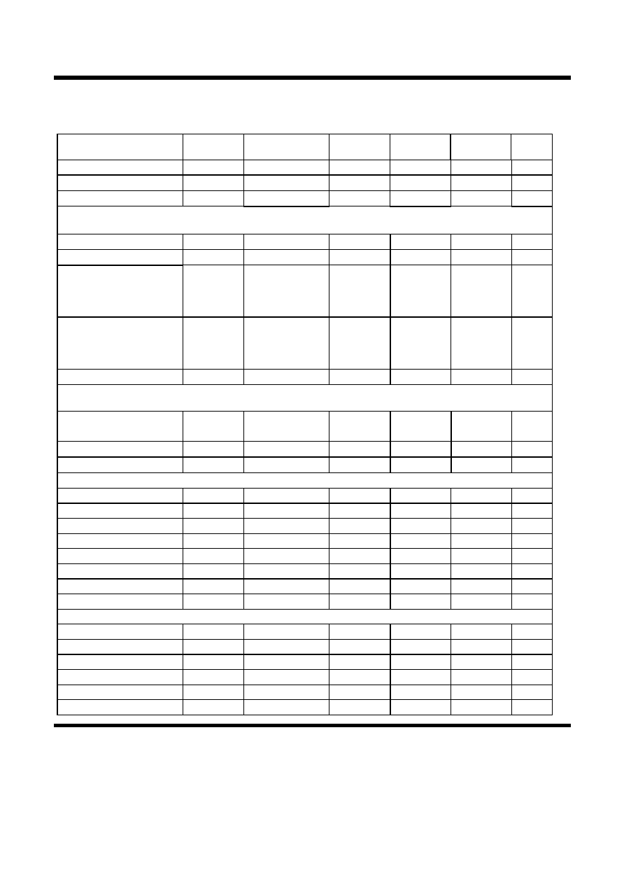
Recommended Operating Conditions
PARAMETER
SYMBOL
TEST
CONDITIONS
MIN
TYP
MAX
UNIT
Supply Voltage
AVDD, DVDD
4.75
5.25
V
Operating Temperature Range
TA
0
70
o
C
Input Common Mode Range
VCMR
0.5
4.5
V

Production Data
WM8143-12
Wolfson Microelectronics
PD. Rev 4 Nov. 99
3
Electrical Characteristics
Test Characteristics
AVDD = DVDD = 4.75V to 5.25V, AGND = DGND = 0V ... T
A
= 0
o
C to +70
o
C, MCLK = 8MHz, unless otherwise stated
PARAMETER
SYMBOL
TEST
CONDITIONS
MIN
TYP
MAX
UNIT
Supply Current - Active 25 40 mA
Supply Current - Standby 4 10 mA
Digital Inputs
High Level Input Voltage
V
IH
0.8*DVDD
V
Low Level Input Voltage
V
IL
0.2*DVDD
V
High Level Input Current
I
IH
1
µA
Low Level Input Current
I
IL
1
µA
Input Capacitance
5
pF
Digital Outputs
High Level Output Voltage
V
OH
I
OH
= 1mA
DVDD-0.75
V
Low Level Output Voltage
V
OL
I
OL
= 1mA
DGND+0.75
V
High Impedance Output
Current
I
OZ
1
µA
Input Multiplexer
CDS Mode Full Scale Input
Range (V
VS
-V
RS
)
x denotes the
channel selected
2
Gx
Vp-p
Channel to Channel Gain
Matching
1
%
Input Video Set-up Time
tVSU
10
ns
Input Video Hold Time
tVH
15
ns
Reset Video Set-up Time
tRSU
CDS Mode only
10
ns
Reset Video Hold Time
tRH
CDS Mode only
15
ns
Reference String
Reference Voltage - Top
VRT
VRU = 5V
3.47
3.5
3.53
V
Reference Voltage - Bottom
VRB
VRU = 5V
1.47
1.5
1.53
V
DAC Reference Voltage
VMID
VRU = 5V
2.47
2.5
2.53
V
R.L.C. Switching Impedance
500
1.46
1.5
1.54
V
2.46
2.5
2.54
V
Reset Level Clamp Options
VRLC
VRU = 5V
Voltage set
by register
configuration
3.46
3.5
3.54
V
Impedance VRT to VRB
250
500
750
Impedance VRU to AGND
1000
1500
2000
8-Bit DACs
Resolution
8
Bits
Zero Code Voltage
V
MID
-20
V
MID
+20
mV
WM8143-12
Production Data
Wolfson Microelectronics
PD. Rev 4 Nov. 99
4
Test Characteristics
AVDD = DVDD = 4.75V to 5.25V, AGND = DGND = 0V ... T
A
= 0
o
C to +70
o
C, MCLK = 8MHz, unless otherwise stated
PARAMETER
SYMBOL
TEST
CONDITIONS
MIN
TYP
MAX
UNIT
Full Scale Voltage Error
0
20
mV
Differential Non Linearity
DNL
0.1
0.5
LSB
Integral Non Linearity
INL
0.25
1
LSB
12-bit ADC performance including CDS, PGA and Offset Functions
NO MISSING CODES GUARANTEED
Resolution
AVDD = DVDD = 5V
12
Bits
Maximum Sampling Rate
AVDD = DVDD = 5V
4
MSPS
Zero Scale Transition Error
Voltage at VINP
DAC Code = 000H,
AVDD = DVDD = 5V,
measured relative to
VRB
± 25
±100
mV
Full Scale Transition Error
Voltage at VINP
DAC Code = 000H,
AVDD = DVDD = 5V,
measured relative to
VRT
± 25
±100
mV
Differential Non Linearity
DNL
AVDD = DVDD = 5V
+1.5
LSB
PGA Gain
Monotonicity Guaranteed
Red Channel Max Gain
Gr
Mode 1
AVDD = DVDD = 5V
7.5
8
Times
Green Channel Max Gain
Gg
7.5
8
Times
Blue Channel Max Gain
Gb
7.5
8
Times
Switching Characteristics
MCLK Period
tPER
125
ns
MCLK High
tCKH
37.5
ns
MCLK Low
tCKL
37.5
ns
Data Set-up Time
tDSU
10
ns
Data Hold Time
tDH
10
ns
Output Propagation Delay
tPD
I
OH
= 1mA, I
OL
= 1mA
75
ns
Output Enable Time
tPZE
50
ns
Output Disable Time
tPEZ
25
ns
Serial Interface
SCK Period
tSPER
125
ns
SCK High
tSCKH
37.5
ns
SCK Low
tSCKL
37.5
ns
SDI Set up Time
tSSU
10
ns
SDI Hold Time
tSH
10
ns
Set up Time - SCK to SEN
tSCE
20
ns

Production Data
WM8143-12
Wolfson Microelectronics
PD. Rev 4 Nov. 99
5
Test Characteristics
AVDD = DVDD = 4.75V to 5.25V, AGND = DGND = 0V ... T
A
= 0
o
C to +70
o
C, MCLK = 8MHz, unless otherwise stated
PARAMETER
SYMBOL
TEST
CONDITIONS
MIN
TYP
MAX
UNIT
Set up Time - SEN to SCK
tSEC
20
ns
SEN Pulse Width
tSEW
50
ns
Parallel Interface
RNW Low to OP[11:4] Tri-
state
tOPZ
20
ns
Address Setup Time to STB
Low
tASU
0
ns
DNA Low Setup Time to STB
Low
tADLS
10
ns
Strobe Low Time
tSTB
50
ns
Address Hold Time from STB
High
tAH
10
ns
DNA Low Hold Time from
STB High
tADLH
10
ns
Data Setup Time to STB Low
tDSU
0
ns
DNA High Setup Time to STB
Low
tADHS
10
ns
Data Hold Time from STB
High
tDH
10
ns
Data High Hold Time from
STB High
tADHH
10
ns
RNW High to OP[11:4]
Output
tOPD
0
ns