Document Outline
- WM8196
- (8 +8) Bit Output 16-bit CIS/CCD AFE/Digitiser
- DESCRIPTION
- FEATURES
- APPLICATIONS
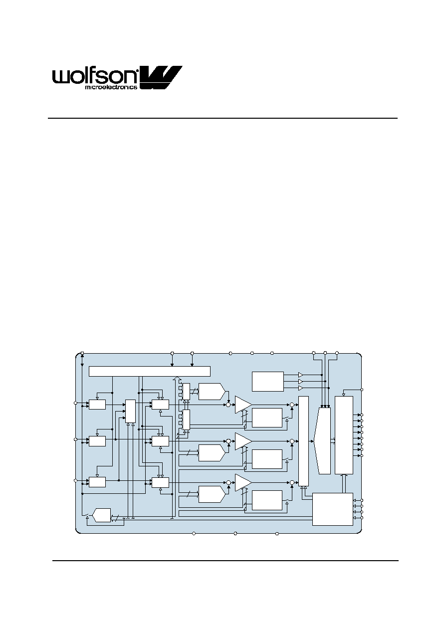
- BLOCK DIAGRAM
- PIN CONFIGURATION
- ORDERING INFORMATION
- PIN DESCRIPTION
- ABSOLUTE MAXIMUM RATINGS
- RECOMMENDED OPERATING CONDITIONS
- ELECTRICAL CHARACTERISTICS
- INPUT VIDEO SAMPLING
- OUTPUT DATA TIMING
- SERIAL INTERFACE
- DEVICE DESCRIPTION
- INTRODUCTION
- INPUT SAMPLING
- RESET LEVEL CLAMPING (RLC)
- CDS/NON-CDS PROCESSING
- OFFSET ADJUST AND PROGRAMMABLE GAIN
- ADC INPUT BLACK LEVEL ADJUST
- OVERALL SIGNAL FLOW SUMMARY
- CALCULATING OUTPUT FOR ANY GIVEN INPUT
- OUTPUT FORMATS
- CONTROL INTERFACE
- TIMING REQUIREMENTS
- PROGRAMMABLE VSMP DETECT CIRCUIT
- REFERENCES
- POWER SUPPLY
- POWER MANAGEMENT
- LINE-BY-LINE OPERATION
- OPERATING MODES
- OPERATING MODE TIMING DIAGRAMS
- DEVICE CONFIGURATION
- REGISTER MAP
- REGISTER MAP DESCRIPTION
- RECOMMENDED EXTERNAL COMPONENTS
- PACKAGE DIMENSIONS
- IMPORTANT NOTICE
WM8196
(8 + 8) Bit Output 16-bit CIS/CCD AFE/Digitiser
WOLFSON MICROELECTRONICS plc
w :: www.wolfsonmicro.com
Production Data, December 2002, Rev 3.0
Copyright
2002 Wolfson Microelectronics plc
DESCRIPTION
The WM8196 is a 16-bit analogue front end/digitiser IC
which processes and digitises the analogue output signals
from CCD sensors or Contact Image Sensors (CIS) at pixel
sample rates of up to 12MSPS.
The device includes three analogue signal processing
channels each of which contains Reset Level Clamping,
Correlated Double Sampling and Programmable Gain and
Offset adjust functions. Three multiplexers allow single
channel processing. The output from each of these
channels is time multiplexed into a single high-speed 16-bit
Analogue to Digital Converter. The digital output data is
available in 8 or 4-bit wide multiplexed format.
An internal 4-bit DAC is supplied for internal reference level
generation. This may be used during CDS to reference CIS
signals or during Reset Level Clamping to clamp CCD
signals. An external reference level may also be supplied.
ADC references are generated internally, ensuring optimum
performance from the device.
Using an analogue supply voltage of 5V and a digital
interface supply of either 5V or 3.3V, the WM8196 typically
only consumes 300mWwhen operating from a single
5V supply.
FEATURES
�
16-bit ADC
�
12MSPS conversion rate
�
Low power � 320mWtypical
�
5V single supply or 5V/3.3V dual supply operation
�
Single or 3 channel operation
�
Correlated double sampling
�
Programmable gain (8-bit resolution)
�
Programmable offset adjust (8-bit resolution)
�
Programmable clamp voltage
�
8 or 4-bit wide multiplexed data output formats
�
Internally generated voltage references
�
28-pin SSOP package
�
Serial control interface
APPLICATIONS
�
Flatbed and sheetfeed scanners
�
USB compatible scanners
�
Multi-function peripherals
�
High-performance CCD sensor interface
BLOCK DIAGRAM
RINP
DATA
I/O
PORT
SEN
VSMP
MCLK
VRLC/VBIAS
SDI
SCK
DVDD2
TIMING CONTROL
CL
RLC/ACYC
RLC
V
S
R
S
BINP
GINP
VRX
VRT
OEB
M
U
X
VRB
RLC
RLC
CDS
CDS
CDS
RLC
DAC
4
CONFIGURABLE
SERIAL
CONTROL
INTERFACE
16-
BIT
ADC
AGND1
DGND
DVDD1
OP[0]
OP[1]
OP[2]
OP[3]
OP[4]
OP[5]
OP[6]
OP[7]/SDO
AGND2
M
U
X
VREF/BIAS
M
U
X
R
G
B
M
U
X
R
G
B
+
PGA
I/P SIGNAL
POLARITY
ADJUST
8
8
PGA
8
8
OFFSET
DAC
PGA
8
OFFSET
DAC
8
+
+
+
+
+
I/P SIGNAL
POLARITY
ADJUST
I/P SIGNAL
POLARITY
ADJUST
AVDD
w
WM8196
OFFSET
DAC
WM8196
Production Data
w
PD Rev 3.0 December 2002
2
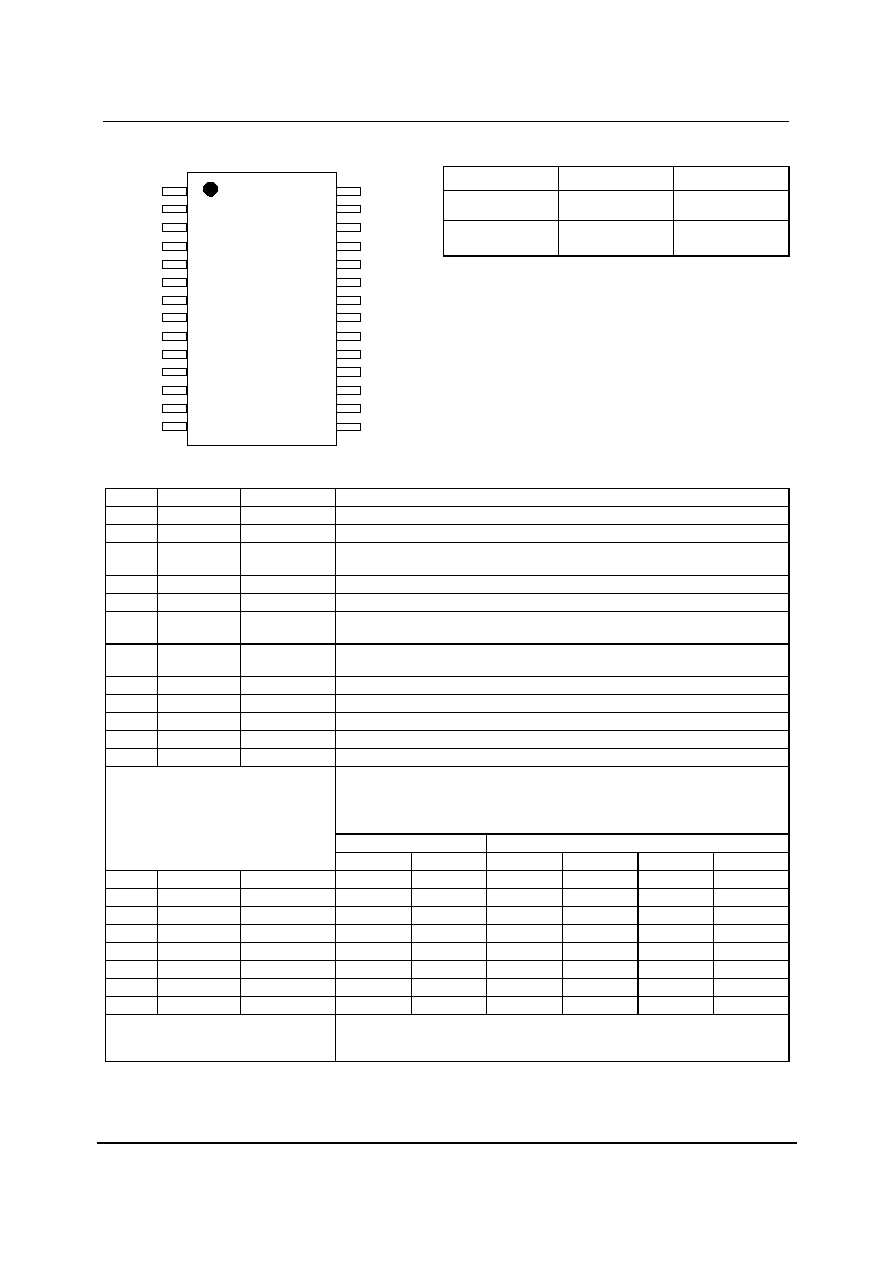
PIN CONFIGURATION
ORDERING INFORMATION
DEVICE
TEMP. RANGE
PACKAGE
WM8196CDS
0 to 70
o
C
28-pin SSOP
WM8196CDS/R
0 to 70
o
C
28-pin SSOP
(tape and reel)
SEN
OP[1]
OP[0]
SCK
SDI
DVDD2
OP[7]/SDO
OP[2]
OP[3]
OP[4]
OP[5]
OP[6]
GINP
AGND1
VRB
VRT
VRX
VRLC/VBIAS
BINP
AVDD
DGND
AGND2
DVDD1
OEB
VSMP
RLC/ACYC
MCLK
RINP
1
2
3
4
5
6
7
8
9
10
11
12
13
14
28
27
26
25
24
23
22
21
20
19
18
17
16
15
Note:
Reel quantity = 2,000
PIN DESCRIPTION
PIN
NAME
TYPE
DESCRIPTION
1
RINP
Analogue input
Red channel input video.
2
AGND2
Supply
Analogue ground (0V).
3
DVDD1
Supply
Digital supply (5V) for logic and clock generator. This must be operated at the same
potential as AVDD.
4
OEB
Digital input
Output Hi-Z control, all digital outputs disabled when OEB = 1.
5
VSMP
Digital input
Video sample synchronisation pulse.
6
RLC/ACYC
Digital input
RLC (active high) selects reset level clamp on a pixel-by-pixel basis � tie high if
used on every pixel. ACYC autocycles between R, G, B inputs.
7
MCLK
Digital input
Master clock. This clock is applied at N times the input pixel rate (N = 2, 3, 6, 8 or
any multiple of 2 thereafter depending on input sample mode).
8
DGND
Supply
Digital ground (0V).
9
SEN
Digital input
Enables the serial interface when high.
10
DVDD2
Supply
Digital supply (5V/3.3V), all digital I/O pins.
11
SDI
Digital input
Serial data input.
12
SCK
Digital input
Serial clock.
Digital multiplexed output data bus.
ADC output data (d15:d0) is available in two multiplexed formats as shown, under
the control of register MUXOP [1:0]
See `Output Formats' description in Device Description section for further details.
8+8-bit
4+4+4+4-bit
A
B
A
B
C
D
13
OP[0]
Digital output
d8
d0
14
OP[1]
Digital output
d9
d1
15
OP[2]
Digital output
d10
d2
16
OP[3]
Digital output
d11
d3
17
OP[4]
Digital output
d12
d4
d12
d8
d4
d0
18
OP[5]
Digital output
d13
d5
d13
d9
d5
d1
19
OP[6]
Digital output
d14
d6
d14
d10
d6
d2
20
OP[7]/SDO
Digital output
d15
d7
d15
d11
d7
d3
Alternatively, pin OP[7]/SDO may be used to output register read-back data when
OEB = 0 and SEN has been pulsed high. See Serial Interface description in Device
Description section for further details.
WM8196
Production Data
w
PD Rev 3.0 December 2002
3
PIN
NAME
TYPE
DESCRIPTION
21
AVDD
Supply
Analogue supply (5V). This must be operated at the same potential as DVDD1.
22
AGND1
Supply
Analogue ground (0V).
23
VRB
Analogue output
Lower reference voltage.
This pin must be connected to AGND via a decoupling capacitor.
24
VRT
Analogue output
Upper reference voltage.
This pin must be connected to AGND via a decoupling capacitor.
25
VRX
Analogue output
Input return bias voltage.
This pin must be connected to AGND via a decoupling capacitor.
26
VRLC/VBIAS
Analogue I/O
Selectable analogue output voltage for RLC or single-ended bias reference.
This pin would typically be connected to AGND via a decoupling capacitor.
VRLC can be externally driven if programmed Hi-Z.
27
BINP
Analogue input
Blue channel input video.
28
GINP
Analogue input
Green channel input video.
ABSOLUTE MAXIMUM RATINGS
Absolute Maximum Ratings are stress ratings only. Permanent damage to the device may be caused by continuously operating at
or beyond these limits. Device functional operating limits and guaranteed performance specifications are given under Electrical
Characteristics at the test conditions specified.
ESD Sensitive Device. This device is manufactured on a CMOS process. It is therefore generically susceptible
to damage from excessive static voltages. Proper ESD precautions must be taken during handling and storage
of this device.
The WM8196 has been classified as MSL1, which has an unlimited floor life at <30
o
C / 85% Relative Humidity and therefore will
not be supplied in moisture barrier bags.
CONDITION
MIN
MAX
Analogue supply voltage: AVDD
GND - 0.3V
GND + 7V
Digital supply voltages: DVDD1
-
2
GND - 0.3V
GND + 7V
Digital ground: DGND
GND - 0.3V
GND + 0.3V
Analogue grounds: AGND1
-
2
GND - 0.3V
GND + 0.3V
Digital inputs, digital outputs and digital I/O pins
GND - 0.3V
DVDD2 + 0.3V
Analogue inputs (RINP, GINP, BINP)
GND - 0.3V
AVDD + 0.3V
Other pins
GND - 0.3V
AVDD + 0.3V
Operating temperature range: T
A
0
�
C
+70
�
C
Storage temperature prior to soldering
30
�
C max / 85% RH max
Storage temperature after soldering
-65
�
C
+150
�
C
Package body temperature (soldering, 10 seconds)
+260
�
C
Package body temperature (soldering, 2 minutes)
+183
�
C
Notes:
1.
GND denotes the voltage of any ground pin.
2.
AGND1, AGND2 and DGND pins are intended to be operated at the same potential. Differential voltages
between these pins will degrade performance.
RECOMMENDED OPERATING CONDITIONS
CONDITION
SYMBOL
MIN
TYP
MAX
UNITS
Operating temperature range
T
A
0
70
�
C
Analogue supply voltage
AVDD
4.75
5.0
5.25
V
Digital core supply voltage
DVDD1
4.75
5.0
5.25
V
5V I/O
DVDD2
4.75
5.0
5.25
V
Digital I/O supply voltage
3.3V I/O
DVDD2
2.97
3.3
3.63
V

WM8196
Production Data
w
PD Rev 3.0 December 2002
4
ELECTRICAL CHARACTERISTICS
Test Conditions
AVDD = DVDD1 = 5.0V, DVDD2 = 3.3V, AGND = DGND = 0V, T
A
= 25
�
C, MCLK = 24MHz unless otherwise stated.
PARAMETER
SYMBOL
TEST
CONDITIONS
MIN
TYP
MAX
UNIT
Overall System Specification (including 16-bit ADC, PGA, Offset and CDS functions)
Conversion Rate
12
MSPS
Full-scale input voltage range
(see Note 1)
0.4
4.08
Vp-p
Vp-p
Input signal limits (see Note 2)
V
IN
0
AVDD
V
Full-scale transition error
Gain = 0dB;
PGA[7:0] = 4B(hex)
20
mV
Zero-scale transition error
Gain = 0dB;
PGA[7:0] = 4B(hex)
20
mV
Differential non-linearity
DNL
1.25
LSB
Integral non-linearity
INL
25
LSB
Channel to channel gain matching
1
%
Total output noise
Min Gain
Max Gain
4.5
14
LSB rms
LSB rms
References
Upper reference voltage
VRT
2.85
V
Lower reference voltage
VRB
1.35
V
Input return bias voltage
VRX
1.4
1.65
1.6
V
Diff. reference voltage (VRT-VRB)
V
RTB
1.5
V
Output resistance VRT, VRB, VRX
1
VRLC/Reset-Level Clamp (RLC)
RLC switching impedance
50
VRLC short-circuit current
2
mA
VRLC output resistance
2
VRLC Hi-Z leakage current
VRLC = 0 to AVDD
1
�
A
RLCDAC resolution
4
bits
RLCDAC step size, RLCDAC = 0
V
RLCSTEP
AVDD=5V
0.25
V/step
RLCDAC step size, RLCDAC = 1
V
RLCSTEP
0.17
V/step
RLCDAC output voltage at
code 0(hex), RLCDACRNG = 0
V
RLCBOT
AVDD=5V
0.39
V
RLCDAC output voltage at
code 0(hex), RLCDACRNG = 1
V
RLCBOT
0.26
V
RLCDAC output voltage at
code F(hex) RLCDACRNG, = 0
V
RLCTOP
AVDD=5V
4.16
V
RLCDAC output voltage at
code F(hex), RLCDACRNG = 1
V
RLCTOP
2.81
V
VRLC deviation
-50
+50
mV
Offset DAC, Monotonicity Guaranteed
Resolution
8
bits
Differential non-linearity
DNL
0.1
0.5
LSB
Integral non-linearity
INL
0.25
1
LSB
Step size
2.04
mV/step
Output voltage
Code 00(hex)
Code FF(hex)
-260
+260
mV
mV
Notes:
1.
Full-scale input voltage denotes the maximum amplitude of the input signal at the specified gain.
2.
Input signal limits are the limits within which the full-scale input voltage signal must lie.

WM8196
Production Data
w
PD Rev 3.0 December 2002
5
Test Conditions
AVDD = DVDD1 = 5.0V, DVDD2 = 3.3V, AGND = DGND = 0V, T
A
= 25
�
C, MCLK = 24MHz unless otherwise stated.
PARAMETER
SYMBOL
TEST
CONDITIONS
MIN
TYP
MAX
UNIT
Programmable Gain Amplifier
Resolution
8
bits
Gain
]
0
:
7
[
PGA
283
208
-
V/V
Max gain, each channel
G
MAX
7.4
V/V
Min gain, each channel
G
MIN
0.74
V/V
Gain error, each channel
1
%
Analogue to Digital Converter
Resolution
16
Bits
Speed
12
MSPS
Full-scale input range
(2*(VRT-VRB))
3
V
DIGITAL SPECIFICATIONS
Digital Inputs
High level input voltage
V
IH
0.8
DVDD2
V
Low level input voltage
V
IL
0.2
DVDD2
V
High level input current
I
IH
1
�
A
Low level input current
I
IL
1
�
A
Input capacitance
C
I
5
pF
Digital Outputs
High level output voltage
V
OH
I
OH
= 1mA
DVDD2 - 0.5
V
Low level output voltage
V
OL
I
OL
= 1mA
0.5
V
High impedance output current
I
OZ
1
�
A
Digital IO Pins
Applied high level input voltage
V
IH
0.8
DVDD2
V
Applied low level input voltage
V
IL
0.2
DVDD2
V
High level output voltage
V
OH
I
OH
= 1mA
DVDD2 - 0.5
V
Low level output voltage
V
OL
I
OL
= 1mA
0.5
V
Low level input current
I
IL
1
�
A
High level input current
I
IH
1
�
A
Input capacitance
C
I
5
pF
High impedance output current
I
OZ
1
�
A
Supply Currents
Total supply current
-
active
(Three channel mode)
MCLK = 24MHz
60
mA
Total supply current
-
active
(Single channel mode)
LINEBYLINE = 1
MCLK = 24MHz
45
mA
Total analogue supply current
-
active (Three channel mode)
I
AVDD
MCLK = 24MHz
56
mA
Total analogue supply current
-
active (One channel mode)
I
AVDD
LINEBYLINE = 1
MCLK = 24MHz
41
mA
Digital core supply current,
DVDD1
-
active (Note1)
MCLK = 24MHz
3
mA
Digital I/O supply current,
DVDD2
-
active (Note1)
MCLK = 24MHz
1
mA
Supply current
-
full power down
mode
300
�
A
WM8196
Production Data
w
PD Rev 3.0 December 2002
6
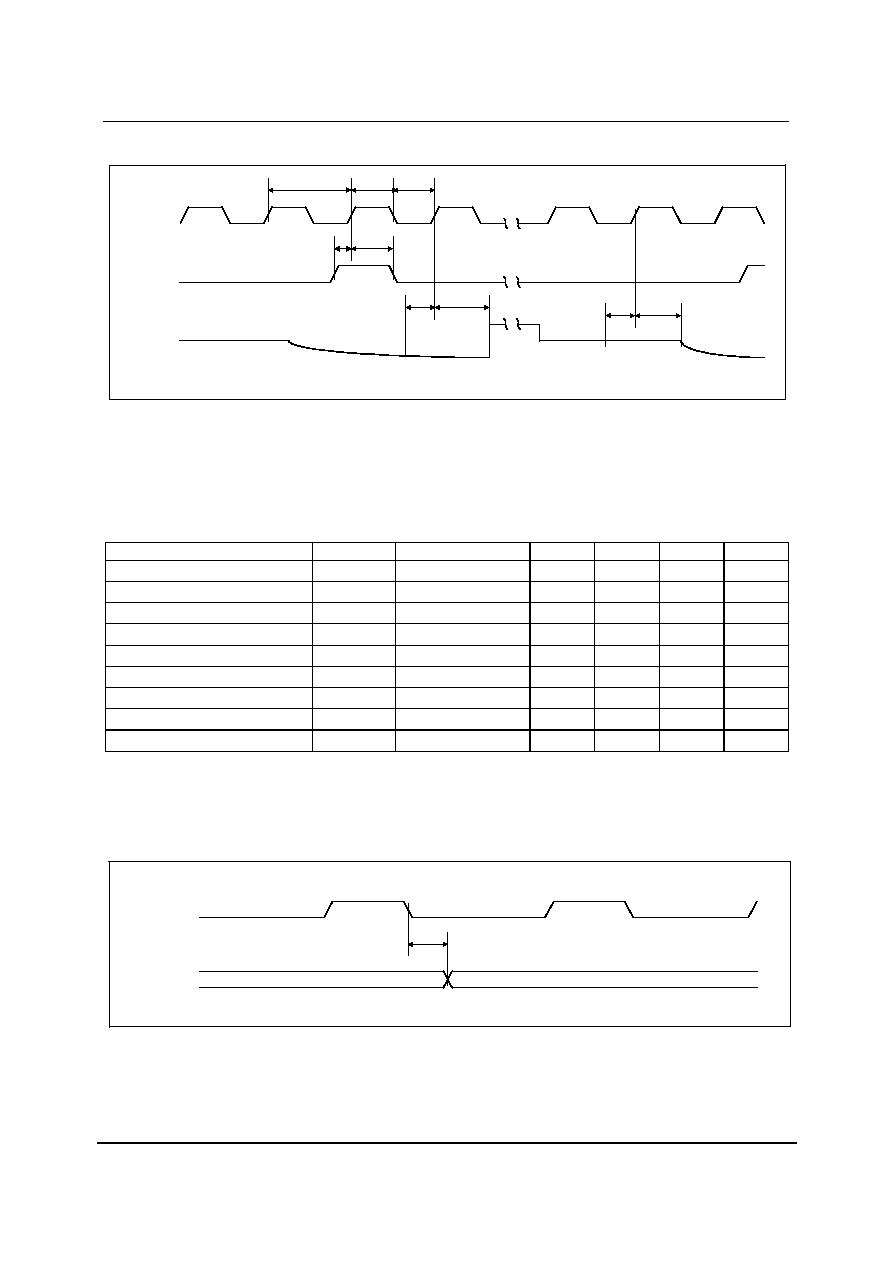
INPUT VIDEO SAMPLING
MCLK
VSMP
INPUT
VIDEO
t
PER
t
VSMPSU
t
VSMPH
t
VSU
t
VH
t
RSU
t
RH
t
MCLKL
t
MCLKH
Figure 1 Input Video Timing
Note:
1.
See Page 14 (Programmable VSMP Detect Circuit) for video sampling description.
Test Conditions
AVDD = DVDD1 = 5.0V, DVDD2 = 3.3V, AGND = DGND = 0V, T
A
= 25
�
C, MCLK = 24MHz unless otherwise stated.
PARAMETER
SYMBOL
TEST CONDITIONS
MIN
TYP
MAX
UNITS
MCLK period
t
PER
41.6
ns
MCLK high period
t
MCLKH
18.8
ns
MCLK low period
t
MCLKL
18.8
ns
VSMP set-up time
t
VSMPSU
6
ns
VSMP hold time
t
VSMPH
3
ns
Video level set-up time
t
VSU
10
ns
Video level hold time
t
VH
3
ns
Reset level set-up time
t
RSU
10
ns
Reset level hold time
t
RH
3
ns
Notes:
1.
t
VSU
and t
RSU
denote the set-up time required after the input video signal has settled.
2.
Parameters are measured at 50% of the rising/falling edge.
OUTPUT DATA TIMING
MCLK
OP[7:0]
t
PD
Figure 2 Output Data Timing

WM8196
Production Data
w
PD Rev 3.0 December 2002
7
OEB
OP[7:0]
t
PZE
Hi-Z
t
PEZ
Hi-Z
Figure 3 Output Data Enable Timing
Test Conditions
AVDD = DVDD1 = 5.0V, DVDD2 = 3.3V, AGND = DGND = 0V, T
A
= 25
�
C, MCLK = 24MHz unless otherwise stated.
PARAMETER
SYMBOL
TEST CONDITIONS
MIN
TYP
MAX
UNITS
Output propagation delay
t
PD
I
OH
= 1mA, I
OL
= 1mA
40
ns
Output enable time
t
PZE
20
ns
Output disable time
t
PEZ
15
ns
MCLK
RLC/ACYC
PGA/OFFSET
MUX OUTPUT
t
ACYCSU
t
ACYCH
t
ACYCSU
t
ACYCH
Figure 4 Auto Cycle Timing
Test Conditions
AVDD = DVDD1 = 5.0V, DVDD2 = 3.3V, AGND = DGND = 0V, T
A
= 25
�
C, MCLK = 24MHz unless otherwise stated.
PARAMETER
SYMBOL
TEST CONDITIONS
MIN
TYP
MAX
UNITS
Auto Cycle set-up time
t
ACYCSU
6
ns
Auto Cycle hold time
t
ACYCH
3
ns

WM8196
Production Data
w
PD Rev 3.0 December 2002
8
SERIAL INTERFACE
SCK
SDI
SEN
SDO
t
SPER
t
SCKL
t
SCKH
t
SSU
t
SH
t
SCE
t
SEW
t
SEC
t
SERD
t
SCRD
MSB
LSB
t
SCRDZ
ADC DATA
ADC
DATA
REGISTER DATA
Figure 5 Serial Interface Timing
Test Conditions
AVDD = DVDD1 = 5.0V, DVDD2 = 3.3V, AGND = DGND = 0V, T
A
= 25
�
C, MCLK = 24MHz unless otherwise stated.
PARAMETER
SYMBOL
TEST CONDITIONS
MIN
TYP
MAX
UNITS
SCK period
t
SPER
41.6
ns
SCK high
t
SCKH
18.8
ns
SCK low
t
SCKL
18.8
ns
SDI set-up time
t
SSU
6
ns
SDI hold time
t
SH
6
ns
SCK to SEN set-up time
t
SCE
12
ns
SEN to SCK set-up time
t
SEC
12
ns
SEN pulse width
t
SEW
25
ns
SEN low to SDO = Register data
t
SERD
30
ns
SCK low to SDO = Register data
t
SCRD
30
ns
SCK low to SDO = ADC data
t
SCRDZ
30
ns
Note:
1. Parameters are measured at 50% of the rising/falling edge

WM8196
Production Data
w
PD Rev 3.0 December 2002
9
DEVICE DESCRIPTION
INTRODUCTION
A block diagram of the device showing the signal path is presented on Page 1.
The WM8196 samples up to three inputs (RINP, GINP and BINP) simultaneously. The device then
processes the sampled video signal with respect to the video reset level or an internally/externally
generated reference level using either one or three processing channels.
Each processing channel consists of an Input Sampling block with optional Reset Level Clamping
(RLC) and Correlated Double Sampling (CDS), an 8-bit programmable offset DAC and an 8-bit
Programmable Gain Amplifier (PGA).
The ADC then converts each resulting analogue signal to a 16-bit digital word. The digital output from
the ADC is presented on an 8-bit wide bi-directional bus, with optional 8 or 4-bit multiplexed formats.
On-chip control registers determine the configuration of the device, including the offsets and gains
applied to each channel. These registers are programmable via a serial interface.
INPUT SAMPLING
The WM8196 can sample and process one to three inputs through one or three processing channels
as follows:
Colour Pixel-by-Pixel: The three inputs (RINP, GINP and BINP) are simultaneously sampled for
each pixel and a separate channel processes each input. The signals are then multiplexed into the
ADC, which converts all three inputs within the pixel period.
Monochrome: A single chosen input (RINP, GINP, or BINP) is sampled, processed by the
corresponding channel, and converted by the ADC. The choice of input and channel can be changed
via the control interface, e.g. on a line-by-line basis if required.
Colour Line-by-Line: A single chosen input (RINP, GINP, or BINP) is sampled and multiplexed into
the red channel for processing before being converted by the ADC. The input selected can be
switched in turn (RINP
GINP
BINP
RINP...) together with the PGA and Offset DAC control
registers by pulsing the RLC/ACYC pin. This is known as auto-cycling. Alternatively, other sampling
sequences can be generated via the control registers. This mode causes the blue and green
channels to be powered down. Refer to the Line-by-Line Operation section for more details.
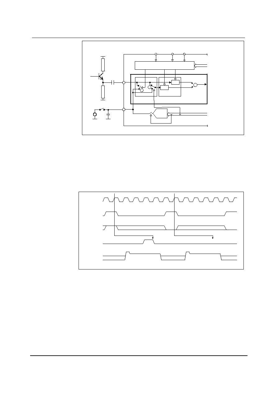
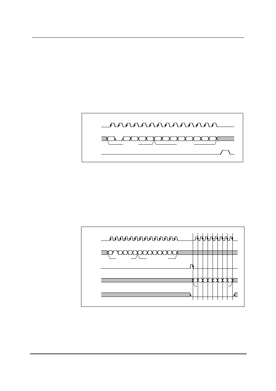
RESET LEVEL CLAMPING (RLC)
To ensure that the signal applied to the WM8196 lies within its input range (0V to AVDD) the CCD
output signal is usually level shifted by coupling through a capacitor, C
IN.
The RLC circuit clamps the
WM8196 side of this capacitor to a suitable voltage during the CCD reset period.
A typical input configuration is shown in Figure 6. A clamp pulse, CL, is generated from MCLK and
VSMP by the Timing Control Block. When CL is active the voltage on the WM8196 side of C
IN
, at
RINP, is forced to the VRLC/VBIAS voltage (V
VRLC
) by switch 1. When the CL pulse turns off, the
voltage at RINP initially remains at V
VRLC
but any subsequent variation in sensor voltage (from reset
to video level) will couple through C
IN
to RINP.
RLC is compatible with both CDS and non-CDS operating modes, as selected by switch 2. Refer to
the CDS/non-CDS Processing section.
WM8196
Production Data
w
PD Rev 3.0 December 2002
10
TIMING CONTROL
S/H
4-BIT
RLC DAC
CL
+
+
-
TO OFFSET DAC
RLC
CDS
FROM CONTROL
INTERFACE
S/H
V
S
R
S
FROM CONTROL
INTERFACE
MCLK
VSMP
RLC/ACYC
INPUT SAMPLING
BLOCK FORRED
CHANNEL
CDS
C
IN
RINP
VRLC/
VBIAS
2
1
EXTERNAL VRLC
VRLCEXT
Figure 6 Reset Level Clamping and CDS Circuitry
If auto-cycling is not required, RLC can be selected by pin RLC/ACYC. Figure 7 illustrates control of
RLC for a typical CCD waveform, with CL applied during the reset period.
The input signal applied to the RLC pin is sampled on the positive edge of MCLK that occurs during
each VSMP pulse. The sampled level, high (or low) controls the presence (or absence) of the internal
CL pulse on the next reset level. The position of CL can be adjusted by using control bits
CDSREF[1:0] (Figure 8).
If auto-cycling is required, pin RLC/ACYC is no longer available for this function and control bit
RLCINT determines whether clamping is applied.
Figure 7 Relationship of RLC Pin, MCLK and VSMP to Internal Clamp Pulse, CL
The VRLC/VBIAS pin can be driven internally by a 4-bit DAC (RLCDAC) by writing to control bits
RLCV[3:0]. The RLCDAC range and step size may be increased by writing to control bit
RLCDACRNG. Alternatively, the VRLC/VBIAS pin can be driven externally by writing to control bit
VRLCEXT to disable the RLCDAC and then applying a d.c. voltage to the pin.
CDS/NON-CDS PROCESSING
For CCD type input signals, the signal may be processed using CDS, which will remove pixel-by-pixel
common mode noise. For CDS operation, the video level is processed with respect to the video reset
level, regardless of whether RLC has been performed. To sample using CDS, control bit CDS must
be set to 1 (default), this controls switch 2 (Figure 6) and causes the signal reference to come from
the video reset level. The time at which the reset level is sampled, by clock R
s
/CL, is adjustable by
programming control bits CDSREF[1:0], as shown in Figure 8.
MCLK
VSMP
ACYC/RLC
or RLCINT
CL
(CDSREF = 01)
INPUT VIDEO
1
X
X
0
X
X
0
RGB
RGB
No RLC on this Pixel
RLC on this Pixel
Programmable Delay
RGB
WM8196
Production Data
w
PD Rev 3.0 December 2002
11
MCLK
VSMP
VS
R
S
/CL (CDSREF = 00)
R
S
/CL (CDSREF = 01)
R
S
/CL (CDSREF = 10)
R
S
/CL (CDSREF = 11)
Figure 8 Reset Sample and Clamp Timing
For CIS type sensor signals, non-CDS processing is used. In this case, the video level is processed
with respect to the voltage on pin VRLC/VBIAS, generated internally or externally as described
above. The VRLC/VBIAS pin is sampled by R
s
at the same time as V
s
samples the video level in this
mode.
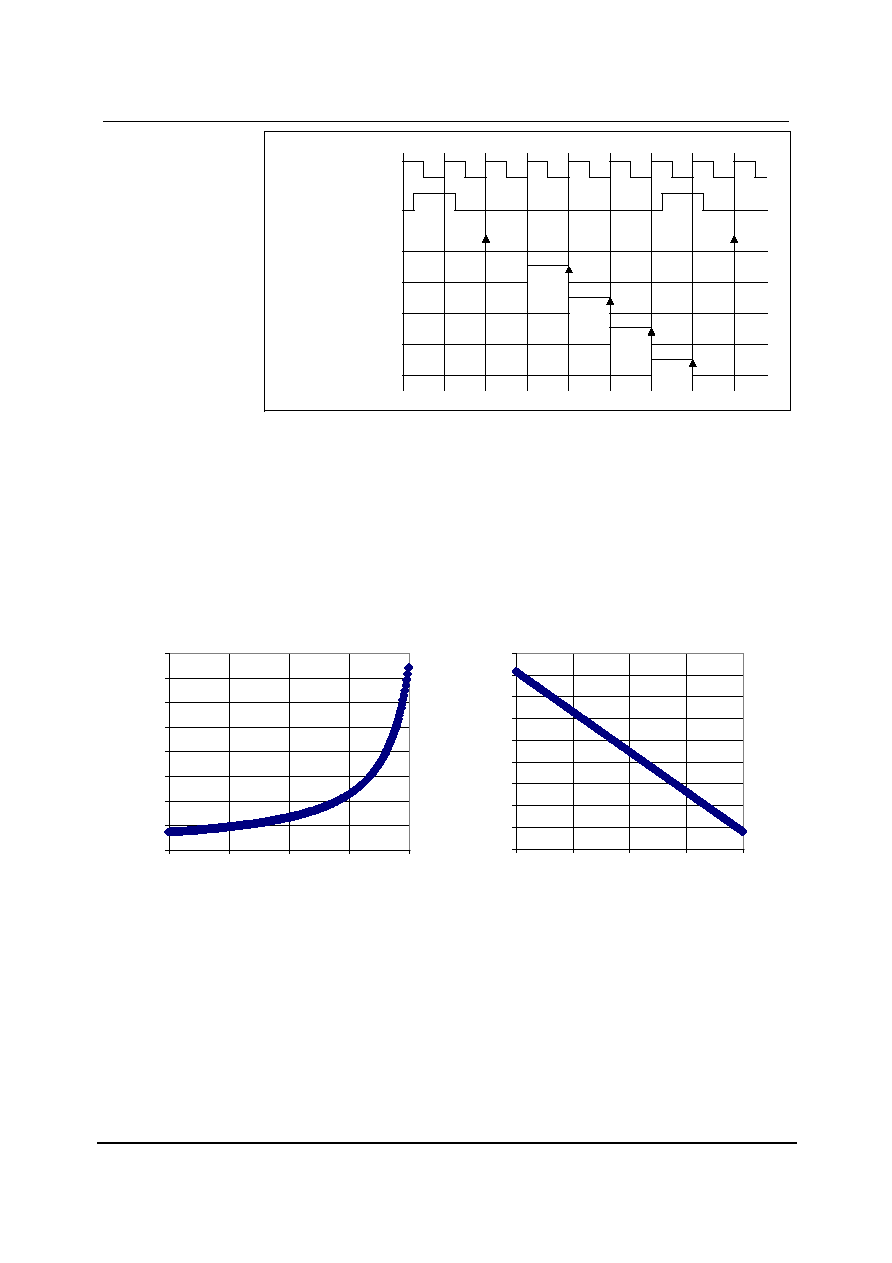
OFFSET ADJUST AND PROGRAMMABLE GAIN
The output from the CDS block is a differential signal, which is added to the output of an 8-bit Offset
DAC to compensate for offsets and then amplified by an 8-bit PGA. The gain and offset for each
channel are independently programmable by writing to control bits DAC[7:0] and PGA[7:0].
The gain characteristic of the WM8196 PGA is shown in Figure 9. Figure 10 shows the maximum
device input voltage that can be gained up to match the ADC full-scale input range (3V).
0
1
2
3
4
5
6
7
8
0
64
128
192
256
Gain register value (PGA[7:0])
PGA
G
a
i
n
(
V/
V)
0
0.5
1
1.5
2
2.5
3
3.5
4
4.5
0
64
128
192
256
Gain register value (PGA[7:0])
P
e
a
k
input
v
o
lta
g
e
t
o
m
a
t
c
h
ADC
Full
-
scale
I
nput
Range
Figure 9 PGA Gain Characteristic
Figure 10 Peak Input Voltage to Match ADC Full-scale Range
In colour line-by-line mode the gain and offset coefficients for each colour can be multiplexed in order
(Red
Green
Blue
Red...) by pulsing the ACYC/RLC pin, or controlled via the FME,
ACYCNRLC and INTM[1:0] bits. Refer to the Line-by-Line Operation section for more details.
WM8196
Production Data
w
PD Rev 3.0 December 2002
12
ADC INPUT BLACK LEVEL ADJUST
The output from the PGA should be offset to match the full-scale range of the ADC (3V). For
negative-going input video signals, a black level (zero differential) output from the PGA should be
offset to the top of the ADC range by setting register bits PGAFS[1:0]=10. For positive going input
signal the black level should be offset to the bottom of the ADC range by setting PGAFS[1:0]=11.
Bipolar input video is accommodated by setting PGAFS[1:0]=00 or PGAFS[1:0]=01 (zero differential
input voltage gives mid-range ADC output).
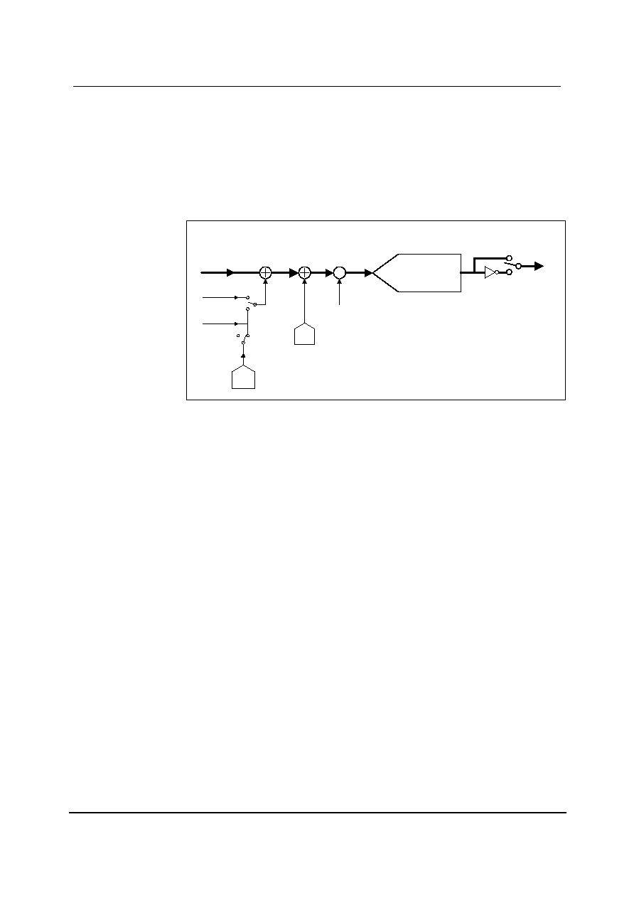
OVER ALL SIGNAL FLOW SUMMAR Y
Figure 11 represents the processing of the video signal through the WM8196.
V
RESET
V
VRLC
V
3
CDS = 1
CDS = 0
RLCEXT=1
260mV*(DAC[7:0]-127.5)/127.5
analog
-
X
+
+
See parametrics for
DAC voltages.
OP[7:0]
D
1
digital
ADC BLOCK
PGA
BLOCK
OFFSET DAC
BLOCK
INPUT
SAMPLING
BLOCK
D
2
CDS, RLCEXT,RLCV[3:0], DAC[7:0],
PGA[7:0], PGAFS[1:0] and INVOP are set
by programming internal control registers.
CDS=1 for CDS, 0 for non-CDS
V
IN
is RINP or GINP or BINP
V
RESET
is V
IN
sampled during reset clamp
VRLC is voltage applied to VRLC pin
V
IN
x (65535/V
FS
)
+0
if PGAFS[1:0]=11
+65535 if PGAFS[1:0]=10
+32768 if PGAFS[1:0]=0x
PGA gain
A = 208/(283-PGA[7:0])
OUTPUT
INVERT
BLOCK
D2 = D1 if INVOP = 0
D2 = 65535-D1 if INVOP = 1
Offset
DAC
RLC
DAC
+
V
2
V
1
RLCEXT=0
Figure 11 Overall Signal Flow
The INPUT SAMPLING BLOCK produces an effective input voltage V
1
. For CDS, this is the
difference between the input video level V
IN
and the input reset level V
RESET
. For non-CDS this is the
difference between the input video level V
IN
and the voltage on the VRLC/VBIAS pin, V
VRLC
,
optionally set via the RLC DAC.
The OFFSET DAC BLOCK then adds the amount of fine offset adjustment required to move the
black level of the input signal towards 0V, producing V
2
.
The PGA BLOCK then amplifies the white level of the input signal to maximise the ADC range,
outputting voltage V
3
.
The ADC BLOCK then converts the analogue signal, V
3
, to a 16-bit unsigned digital output, D
1
.
The digital output is then inverted, if required, through the OUTPUT INVERT BLOCK to produce D
2.
CALCULATING OUTPUT FORANY GIVEN INPUT
The following equations describe the processing of the video and reset level signals through
the WM8196.
INPUT SAMPLING BLOCK: INPUT SAMPLING AND REFERENCING
If CDS = 1, (i.e. CDS operation) the previously sampled reset level, V
RESET
, is subtracted from the
input video.
V
1
=
V
IN
- V
RESET
...................................................................
Eqn. 1
If CDS = 0, (non-CDS operation) the simultaneously sampled voltage on pin VRLC is subtracted
instead.
V
1
=
V
IN
- V
VRLC
....................................................................
Eqn. 2
If RLCEXT = 1, V
VRLC
is an externally applied voltage on pin VRLC/VBIAS.
If RLCEXT = 0, V
VRLC
is the output from the internal RLC DAC.
V
VRLC
=
(V
RLCSTEP
RLCV[3:0]) + V
RLCBOT
.................................
Eqn. 3
WM8196
Production Data
w
PD Rev 3.0 December 2002
13
V
RLCSTEP
is the step size of the RLC DAC and V
RLCBOT
is the minimum output of the RLC DAC.
OFFSET DAC BLOCK: OFFSET (BLACK-LEVEL) ADJUST
The resultant signal V
1
is added to the Offset DAC output.
V
2
=
V
1
+ {260mV
(DAC[7:0]-127.5) } / 127.5 .....................
Eqn. 4
PGA NODE: GAIN ADJUST
The signal is then multiplied by the PGA gain,
V
3
=
V
2
208/(283- PGA[7:0]) ..............................................
Eqn. 5
ADC BLOCK: ANALOGUE-DIGITAL CONVERSION
The analogue signal is then converted to a 16-bit unsigned number, with input range configured by
PGAFS[1:0].
D
1
[15:0] = INT{ (V
3
/V
FS
)
65535} + 32767 PGAFS[1:0] = 00 or 01 ......
Eqn. 6
D
1
[15:0] = INT{ (V
3
/V
FS
)
65535}
PGAFS[1:0] = 11 ...............
Eqn. 7
D
1
[15:0] = INT{ (V
3
/V
FS
)
65535} + 65535 PGAFS[1:0] = 10 ...............
Eqn. 8
where the ADC full-scale range, V
FS
= 3V
OUTPUT INVERT BLOCK: POLARITY ADJUST
The polarity of the digital output may be inverted by control bit INVOP.
D
2
[15:0] = D
1
[15:0]
(INVOP = 0) ......................
Eqn. 9
D
2
[15:0] = 65535 � D
1
[15:0]
(INVOP = 1) ......................
Eqn. 10
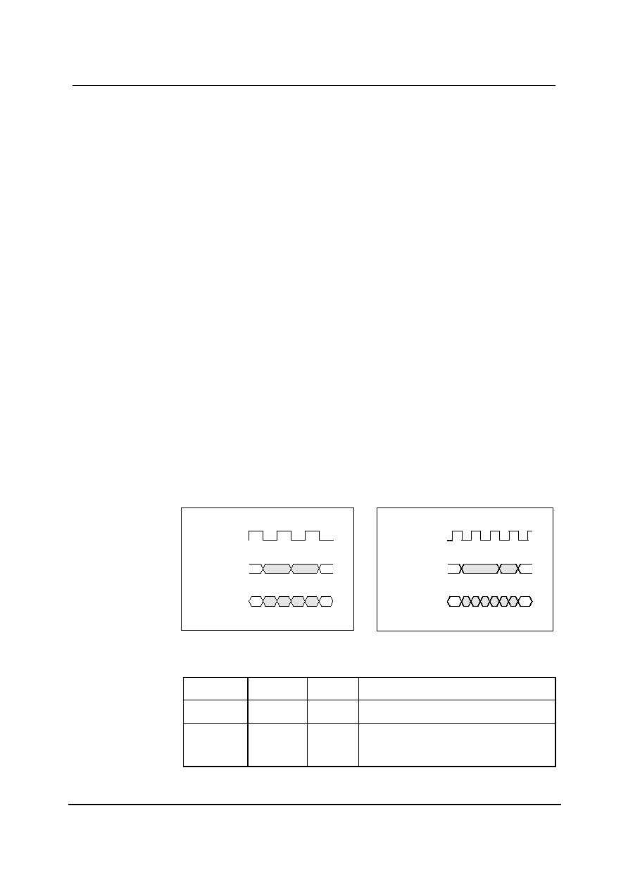
OUTPUT FORMATS
The digital data output from the ADC is available to the user in 8 or 4-bit wide multiplexed formats by
setting control bit MUXOP[1:0]. Latency of valid output data with respect to VSMP is programmable
by writing to control bits DEL[1:0]. The latency for each mode is shown in the Operating Mode Timing
Diagrams section.
Figure 12 shows the output data formats for Modes 1 � 2 and 4 � 6. Figure 13 shows the output data
formats for Mode 3. Table 1 summarises the output data obtained for each format.
MCLK
4+4+4+4-BIT
OUTPUT
A
B
A
B
C
D
8+8-BIT
OUTPUT
MCLK
4+4+4+4-BIT
OUTPUT
A
B
8+8-BIT
OUTPUT
A B
C D
A B
Figure 12 Output Data Formats
(Modes 1
-
-
-
-
2, 4
-
-
-
-
6)
Figure 13 Output Data Formats
(Mode 3)
OUTPUT
FORMAT
MUXOP[1:0]
OUTPUT
PINS
OUTPUT
8+8-bit
multiplexed
00, 01, 10
OP[7:0]
A = d15, d14, d13, d12, d11, d10, d9, d8
B = d7, d6, d5, d4, d3, d2, d1,d0
4+4+4+4-bit
(nibble)
11
OP[7:4]
A = d15, d14, d13, d12
B = d11, d10, d9, d8
C = d7, d6, d5, d4
D = d3, d2, d1, d0
Table 1 Details of Output Data Shown in Figure 12 and Figure 13.
WM8196
Production Data
w
PD Rev 3.0 December 2002
14
CONTROL INTERFACE
The internal control registers are programmable via the serial digital control interface. The register
contents can be read back via the serial interface on pin OP[7]/SDO.
It is recommended that a software reset is carried out after the power-up sequence, before writing to
any other register. This ensures that all registers are set to their default values (as shown in Table
5).
SERIAL INTERFACE: REGISTER WRITE
Figure 14 shows register writing in serial mode. Three pins, SCK, SDI and SEN are used. A six-bit
address (a5, 0, a3, a2, a1, a0) is clocked in through SDI, MSB first, followed by an eight-bit data
word (b7, b6, b5, b4, b3, b2, b1, b0), also MSB first. Each bit is latched on the rising edge of SCK.
When the data has been shifted into the device, a pulse is applied to SEN to transfer the data to the
appropriate internal register. Note all valid registers have address bit a4 equal to 0 in write mode.
SCK
SEN
SDI
a5
0
a3
a2
a1
a0
b7
b6
b5
b4
b3
b2
b1
b0
Address
Data Word
Figure 14 Serial Interface Register Write
A software reset is carried out by writing to Address "000100" with any value of data, i.e. Data Word
= XXXXXXXX.
SERIAL INTERFACE: REGISTER READ-BACK
Figure 15 shows register read-back in serial mode. Read-back is initiated by writing to the serial bus
as described above but with address bit a4 set to 1, followed by an 8-bit dummy data word. Writing
address (a5, 1, a3, a2, a1, a0) will cause the contents (d7, d6, d5, d4, d3, d2, d1, d0) of
corresponding register (a5, 0, a3, a2, a1, a0) to be output MSB first on pin SDO (on the falling edge
of SCK). Note that pin SDO is shared with an output pin, OP[7], therefore OEB should always be
held low when register read-back data is expected on this pin. The next word may be read in to SDI
while the previous word is still being output on SDO.
SCK
SEN
SDI
a5
1
a3 a2 a1 a0
x
x
x
x
x
x
x
x
Address
Data Word
d7 d6 d5 d4 d3 d2 d1 d0
Output Data Word
SDO/
OP[7]
OEB
Figure 15 Serial Interface Register Read-back

WM8196
Production Data
w
PD Rev 3.0 December 2002
15
TIMING REQUIREMENTS
To use this device a master clock (MCLK) of up to 24MHz and a per-pixel synchronisation clock
(VSMP) of up to 12MHz are required. These clocks drive a timing control block, which produces
internal signals to control the sampling of the video signal. MCLK to VSMP ratios and maximum
sample rates for the various modes are shown in Table 4.
PROGRAMMABLE VSMP DETECT CIRCUIT
The VSMP input is used to determine the sampling point and frequency of the WM8196. Under
normal operation a pulse of 1 MCLK period should be applied to VSMP at the desired sampling
frequency (as shown in the Operating Mode Timing Diagrams) and the input sample will be taken on
the first rising MCLK edge after VSMP has gone low. However, in certain applications such a signal
may not be readily available. The programmable VSMP detect circuit in the WM8196 allows the
sampling point to be derived from any signal of the correct frequency, such as a CCD shift register
clock, when applied to the VSMP pin.
When enabled, by setting the VSMPDET control bit, the circuit detects either a rising or falling edge
(determined by POSNNEG control bit) on the VSMP input pin and generates an internal VSMP pulse.
This pulse can optionally be delayed by a number of MCLK periods, specified by the VDEL[2:0] bits.
Figure 16 shows the internal VSMP pulses that can be generated by this circuit for a typical clock
input signal. The internal VSMP pulse is then applied to the timing control block in place of the
normal VSMP pulse provided from the input pin. The sampling point then occurs on the first rising
MCLK edge after this internal VSMP pulse, as shown in the Operating Mode Timing Diagrams.
MCLK
VSMP
(VDEL = 000) INTVSMP
POSNNEG = 1
(VDEL = 001) INTVSMP
(VDEL = 010) INTVSMP
(VDEL = 011) INTVSMP
(VDEL = 100) INTVSMP
(VDEL = 101) INTVSMP
(VDEL = 110) INTVSMP
(VDEL = 111) INTVSMP
POSNNEG = 0
(VDEL = 000) INTVSMP
(VDEL = 001) INTVSMP
(VDEL = 010) INTVSMP
(VDEL = 011) INTVSMP
(VDEL = 100) INTVSMP
(VDEL = 101) INTVSMP
(VDEL = 110) INTVSMP
(VDEL = 111) INTVSMP
INPUT
PINS
V
S
V
S
V
S
V
S
V
S
V
S
V
S
V
S
V
S
V
S
V
S
V
S
V
S
V
S
V
S
V
S
V
S
V
S
V
S
V
S
V
S
V
S
V
S
V
S
V
S
V
S
V
S
V
S
V
S
V
S
V
S
V
S
V
S
V
S
V
S
V
S
V
S
V
S
V
S
V
S
V
S
V
S
V
S
V
S
V
S
V
S
V
S
V
S
Figure 16 Internal VSMP Pulses Generated by Programmable VSMP Detect Circuit

WM8196
Production Data
w
PD Rev 3.0 December 2002
16
REFERENCES
The ADC reference voltages are derived from an internal bandgap reference, and buffered to pins
VRT and VRB, where they must be decoupled to ground. Pin VRX is driven by a similar buffer, and
also requires decoupling. The output buffer from the RLCDAC also requires decoupling at pin
VRLC/VBIAS
POWERSUPPLY
The WM8196 can run from a 5V single supply or from split 5V (core) and 3.3V (digital interface)
supplies.
POWERMANAGEMENT
Power management for the device is performed via the Control Interface. The device can be powered
on or off completely setting by the EN bit and SELPD bit low. Alternatively, when control bit SELPD is
high, only blocks selected by further control bits (SELDIS[3:0]) are powered down. This allows the
user to optimise power dissipation in certain modes, or to define an intermediate standby mode to
allow a quicker recovery into a fully active state. In Line-by-line operation, the green and blue channel
PGAs are automatically powered down.
All the internal registers maintain their previously programmed value in power down modes and the
Control Interface inputs remain active. Table 2 summarises the power down control bit functions.
EN
SELDPD
0
0
Device completely powers down.
1
0
Device completely powers up.
X
1
Blocks with respective SELDIS[3:0] bit high are disabled.
Table 2 Power Down Control
LINE-BY-LINE OPERATION
Certain linear sensors (e.g. Contact Image Sensors) give colour output on a line-by-line basis. i.e. a
full line of red pixels followed by a line of green pixels followed by a line of blue pixels. In order to
accommodate this type of signal the WM8196 can be set into Monochrome mode, with the input
channel switched by writing to control bits CHAN[1:0] between every line. Alternatively, the WM8196
can be placed into colour line-by-line mode by setting the LINEBYLINE control bit. When this bit is
set the green and blue processing channels are powered down and the device is forced internally to
only operate in MONO mode (because only one colour is sampled at a time) through the red channel.
Figure 17 shows the signal path when operating in colour line-by-line mode.
RINP
SEN/STB
VSMP
MCLK
VRLC/VBIAS
SDI/DNA
SCK/RNW
RLC/ACYC
RLC
BINP
GINP
INPUT
MUX
OFFSET
MUX
RLC
R
G
B
R
G
B
PGA
I/P SIGNAL
POLARITY
ADJUST
8
RLC
DAC
+
CONFIGURABLE
SERIAL/
PARALLEL
CONTROL
INTERFACE
OP[7:0]
+
16-
BIT
ADC
DATA
I/O
PORT
8
OFFSET
DAC
PGA
MUX
TIMING CONTROL
CL
V
S
R
S
4
CDS
RLC
NRESET
Figure 17 Signal Path When in Line-by-Line Mode
WM8196
Production Data
w
PD Rev 3.0 December 2002
17
In this mode the input multiplexer and (optionally) the PGA/Offset register multiplexers can be auto-
cycled by the application of pulses to the RLC/ACYC input pin by setting the ACYCNRLC register bit.
See Figure 4 fir detailed timing information.The multiplexers change on the first MCLK rising edge
after RLC/ACYC is taken high. A write to the auto-cycle reset register causes these multiplexers to
be reset; selecting the RINP pin and the RED offset/gain registers. Alternatively, all three
multiplexers can be controlled via the serial interface by writing to register bits INTM[1:0] to select the
desired colour. It is also possible for the input multiplexer to be controlled separately from the PGA
and Offset multiplexers. Table 3 describes all the multiplexer selection modes that are possible.
FME
ACYCNRLC
NAME
DESCRIPTION
0
0
Internal,
no force mux
Input mux, offset and gain registers determined by
internal register bits INTM1, INTM0.
0
1
Auto-cycling,
no force mux
Input mux, offset and gain registers auto-cycled, RINP
GINP
BINP
RINP... on RLC/ACYC pulse.
1
0
Internal,
force mux
Input mux selected from internal register bits FM1, FM0;
Offset and gain registers selected from internal register
bits INTM1, INTM0.
1
1
Auto-cycling,
force mux
Input mux selected from internal register bits FM1, FM0;
Offset and gain registers auto-cycled, RED
GREEN
BLUE
RED... on RLC/ACYC pulse.
Table 3 Colour Selection Description in Line-by-Line Mode

WM8196
Production Data
w
PD Rev 3.0 December 2002
18
OPERATING MODES
Table 4 summarises the most commonly used modes, the clock waveforms required and the register
contents required for CDS and non-CDS operation.
MODE
DESCRIPTION
CDS
AVAILABLE
MAX
SAMPLE
RATE
SENSOR
INTERFACE
DESCRIPTION
TIMING
REQUIRE-
MENTS
REGISTER
CONTENTS
WITH CDS
REGISTER
CONTENTS
WITHOUT CDS
1
Colour
Pixel-by-Pixel
Yes
4MSPS
The 3 input
channels are
sampled in
parallel. The
signal is then
gain and offset
adjusted before
being
multiplexed into
a single data
stream and
converted by the
ADC, giving an
output data rate
of 12MSPS max.
MCLK max =
24MHz
MCLK: VSMP
ratio is 6:1
SetReg1:
03(hex)
SetReg1: 01(hex)
2
Monochrome/
Colour
Line-by-Line
Yes
4MSPS
As mode 1
except:
Only one input
channel at a time
is continuously
sampled.
MCLK max =
24MHz
MCLK: VSMP
ratio is 6:1
SetReg1:
07(hex)
SetReg1: 05(hex)
3
Fast
Monochrome/
Colour
Line-by-Line
Yes
8MSPS
Identical to mode
2
MCLK max =
24MHz
MCLK: VSMP
ratio is 3:1
Identical to
mode 2 plus
SetReg3:
bits 5:4 must
be set to
0(hex)
Identical to
mode 2
4
Maximum
speed
Monochrome/
Colour
Line-by-Line
No
12MSPS
Identical to mode
2
MCLK max =
24MHz
MCLK: VSMP
ratio is 2:1
CDS not
possible
SetReg1: 45(hex)
5
Slow Colour
Pixel-by-Pixel
Yes
3MSPS
Identical to mode
1
MCLK max =
24MHz
MCLK: VSMP
ratio is
2n:1, n
4
Identical to
mode 1
Identical to
mode 1
6
Slow
Monochrome/
Colour
Line-by-Line
Yes
3MPS
Identical to mode
2
MCLK max =
24MHz
MCLK: VSMP
ratio is
2n:1, n
4
Identical to
mode 2
Identical to
mode 2
Table 4 WM8196 Operating Modes
Notes:
1.
In Monochrome mode, SetReg3 bits 7:6 determine which input is to be sampled.
2.
For Colour Line-by-Line, set control bit LINEBYLINE. For input selection, refer to Table 4, Colour Selection
Description in Line-by-Line Mode.

WM8196
Production Data
w
PD Rev 3.0 December 2002
19
OPERATING MODE TIMING DIAGRAMS
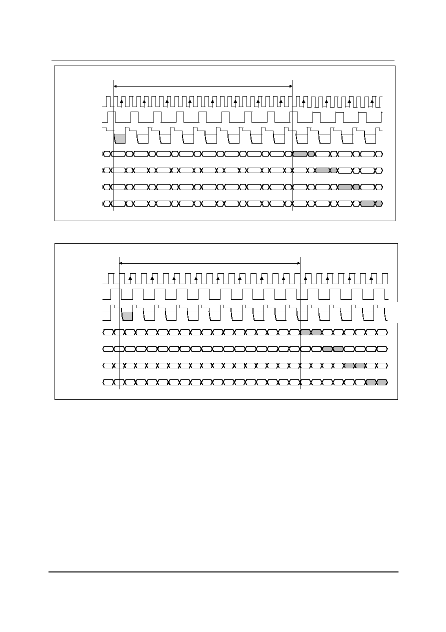
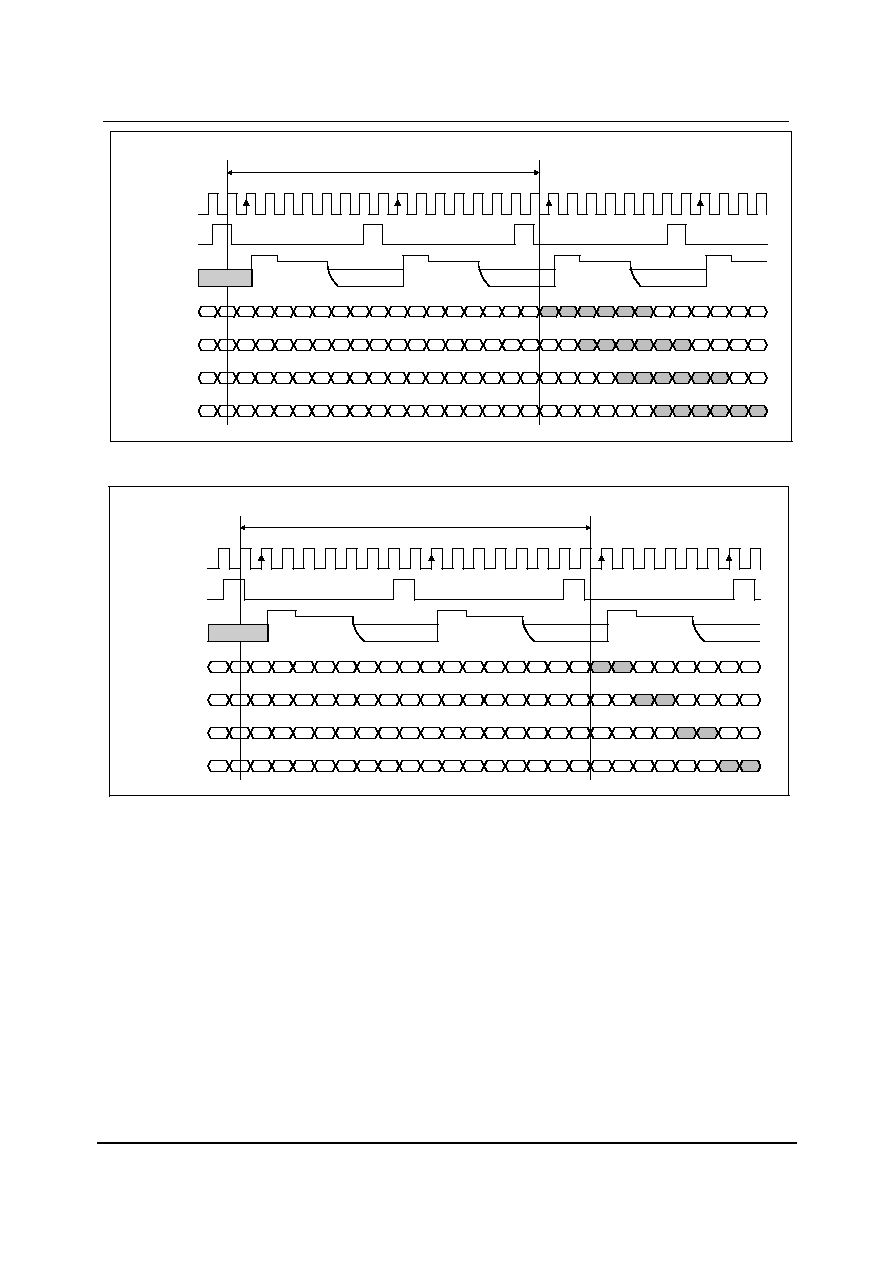
The following diagrams show 8-bit multiplexed output data and MCLK, VSMP and input video
requirements for operation of the most commonly used modes as shown in Table 4. The diagrams
are identical for both CDS and non-CDS operation. Outputs from RINP, GINP and BINP are shown
as R, G and B respectively. X denotes invalid data.
MCLK
VSMP
INPUT VIDEO
OP[7:0]
(DEL = 00)
16.5 MCLK PERIODS
R
A
R
B
G
A
G
B
B
A
B
B
R
A
R
B
G
A
G
B
B
A
B
B
R
A
R
B
G
A
G
B
B
A
B
B
R
A
R
B
R
A
R
B
G
A
G
B
B
A
B
B
OP[7:0]
(DEL = 01)
B
A
B
B
R
A
R
B
G
A
G
B
B
A
B
B
R
A
R
B
G
A
G
B
B
A
B
B
R
A
R
B
G
A
G
B
B
A
B
B
B
A
B
B
R
A
R
B
G
A
G
B
OP[7:0]
(DEL = 10)
G
A
G
B
B
A
B
B
R
A
R
B
G
A
G
B
B
A
B
B
R
A
R
B
G
A
G
B
B
A
B
B
R
A
R
B
G
A
G
B
G
A
G
B
B
A
B
B
R
A
R
B
OP[7:0]
(DEL = 11)
R
A
R
B
G
A
G
B
B
A
B
B
R
A
R
B
G
A
G
B
B
A
B
B
R
A
R
B
G
B
G
A
B
A
B
B
R
A
R
B
R
A
R
B
G
A
G
B
B
A
B
B
B
A
B
B
G
A
G
B
B
A
B
B
R
A
R
B
R
A
R
B
G
A
G
B
G
A
G
B
B
A
B
B
Figure 18 Mode 1 Operation
16.5 MCLK PERIODS
X
MCLK
VSMP
INPUT VIDEO
OP[7:0] (DEL = 00)
R
A
R
B
X
X
X
R
A
R
B
X
X
X
X
R
A
R
B
X
X
X
X
R
A
R
B
X
X
X
X
R
A
R
B
OP[7:0] (DEL = 01)
X
X
X
X
X
X
X
X
X
X
X
X
X
X
X
X
X
X
X
OP[7:0] (DEL = 10)
X
X
X
X
X
X
X
X
X
X
X
X
X
X
X
X
X
X
OP[7:0] (DEL = 11)
R
A
R
B
X
X
X
R
A
R
B
X
X
X
X
R
A
R
B
X
X
X
X
R
A
R
B
X
X
X
X
R
A
R
B
R
A
R
B
R
A
R
B
R
A
R
B
R
A
R
B
R
A
R
B
R
A
R
B
R
A
R
B
R
A
R
B
Figure 19 Mode 2 Operation
WM8196
Production Data
w
PD Rev 3.0 December 2002
20
MCLK
VSMP
OP[7:0]
(DEL = 00)
INPUT VIDEO
OP[7:0]
(DEL = 01)
OP[7:0]
(DEL = 10)
OP[7:0]
(DEL = 11)
23.5 MCLK PERIODS
R
B
R
A
R
B
R
A
R
B
R
A
R
B
R
A
R
B
R
A
R
B
R
A
R
B
R
A
R
B
R
A
R
B
R
A
R
B
R
B
R
A
R
B
R
A
R
B
R
A
R
B
R
A
R
B
R
A
R
B
R
A
R
B
R
A
R
B
R
A
R
B
R
B
R
A
R
B
R
A
R
B
R
A
R
B
R
A
R
B
R
A
R
B
R
A
R
B
R
A
R
B
R
A
R
B
R
A
R
B
R
B
R
A
R
B
R
A
R
B
R
A
R
B
R
A
R
B
R
A
R
B
R
A
R
B
R
A
R
B
R
A
R
B
R
A
R
B
R
A
R
B
R
A
R
B
R
A
R
B
R
A
R
B
R
A
R
B
R
A
R
B
R
A
R
B
R
A
R
B
R
A
R
B
R
A
R
B
R
A
R
B
R
A
R
B
R
A
R
B
Figure 20 Mode 3 Operation
MCLK
VSMP
INPUT VIDEO
OP[7:0]
(DEL = 00)
16.5 MCLK PERIODS
R
A
R
B
R
A
R
B
R
A
R
B
R
A
R
B
R
A
R
B
R
A
R
B
R
A
R
B
R
A
R
B
R
A
R
B
R
A
R
B
R
A
R
B
OP[7:0]
(DEL = 01)
R
A
R
B
R
A
R
B
R
A
R
B
R
A
R
B
R
A
R
B
R
A
R
B
R
A
R
B
R
A
R
B
R
A
R
B
R
A
R
B
R
A
R
B
OP[7:0]
(DEL = 10)
R
A
R
B
R
A
R
B
R
A
R
B
R
A
R
B
R
A
R
B
R
A
R
B
R
A
R
B
R
A
R
B
R
A
R
B
R
A
R
B
R
A
R
B
OP[7:0]
(DEL = 11)
R
A
R
B
R
A
R
B
R
A
R
B
R
A
R
B
R
A
R
B
R
A
R
B
R
A
R
B
R
A
R
B
R
A
R
B
R
A
R
B
R
A
R
B
R
A
R
B
R
A
R
B
R
A
R
B
R
A
R
B
R
A
R
B
R
A
R
B
R
A
R
B
R
A
R
B
Figure 21 Mode 4 Operation
WM8196
Production Data
w
PD Rev 3.0 December 2002
21
16.5 MCLK PERIODS
MCLK
VSMP
INPUT
VIDEO
OP[7:0]
(DEL = 00)
X
X
R
A
R
B
G
A
G
B
B
A
B
B
X
X
R
A
R
B
G
A
G
B
B
A
B
B
X
X
R
A
R
B
G
A
G
B
B
A
B
B
OP[7:0]
(DEL = 01)
X
X
R
A
R
B
G
A
G
B
B
A
B
B
X
X
R
A
R
B
G
A
G
B
B
A
B
B
X
X
R
A
R
B
G
A
G
B
B
A
B
B
OP[7:0]
(DEL = 10)
X
X
R
A
R
B
G
A
G
B
B
A
B
B
X
X
R
A
R
B
G
A
G
B
B
A
B
B
X
X
R
A
R
B
G
A
G
B
B
A
B
B
OP[7:0]
(DEL = 11)
X
X
R
A
R
B
G
A
G
B
B
A
B
B
X
X
R
A
R
B
G
A
G
B
B
A
B
B
X
X
R
A
R
B
G
A
G
B
B
A
B
B
B
A
B
B
X
X
G
A
G
B
B
A
B
B
R
A
R
B
G
A
G
B
B
A
B
B
X
X
X
X
R
A
R
B
R
A
R
B
G
A
G
B
Figure 22 Mode 5 Operation (MCLK:VSMP Ratio = 8:1)
16.5 MCLK PERIODS
MCLK
VSMP
INPUT VIDEO
OP[7:0]
(DEL = 00)
X
X
R
A
R
B
X
X
X
X
X
X
R
A
R
B
X
X
X
X
X
X
R
A
R
B
X
X
X
X
X
X
OP[7:0]
(DEL = 01)
X
X
R
A
R
B
X
X
X
X
R
A
R
B
X
X
X
X
R
A
R
B
X
X
X
X
OP[7:0]
(DEL = 10)
X
X
R
A
R
B
X
X
X
X
X
X
X
X
R
A
R
B
X
X
X
X
OP[7:0]
(DEL = 11)
R
A
R
B
X
X
X
X
X
X
X
X
X
X
X
X
X
X
X
X
X
X
X
X
R
A
R
B
X
X
R
A
R
B
X
X
R
A
R
B
X
X
X
X
X
X
R
A
R
B
Figure 23 Mode 6 Operation (MCLK:VSMP Ratio = 8:1)

WM8196
Production Data
w
PD Rev 3.0 December 2002
22
DEVICE CONFIGURATION
REGISTER MAP
The following table describes the location of each control bit used to determine the operation of the
WM8196. The register map is programmed by writing the required codes to the appropriate
addresses via the serial interface.
BIT
ADDRESS
<a5:a0>
DESCRIPTION
DEF
(hex)
RW
b7
b6
b5
b4
b3
b2
b1
b0
000001
Setup Reg 1
03
RW
MODE4
PGAFS[1]
PGAFS[0]
SELPD
MONO
CDS
EN
000010
Setup Reg 2
20
RW
DEL[1]
DEL[0]
RLCDACRNG
0
VRLCEXT
INVOP
MUXOP[1]
MUXOP[0]
000011
Setup Reg 3
1F
RW
CHAN[1]
CHAN[0]
CDSREF [1]
CDSREF [0]
RLCV[3]
RLCV[2]
RLCV[1]
RLCV[0]
000100
Software Reset
00
W
000101
Auto-cycle Reset
00
W
000110
Setup Reg 4
00
RW
FM[1]
FM[0]
INTM[1]
INTM[0]
RLCINT
FME
ACYCNRLC
LINEBYLINE
000111
Revision Number
41
R
001000
Setup Reg 5
00
RW
0
0
0
POSNNEG
VDEL[2]
VDEL[1]
VDEL[0]
VSMPDET
001001
Setup Reg 6
00
RW
0
0
0
0
SELDIS[3]
SELDIS[2]
SELDIS[1]
SELDIS[0]
001010
Reserved
00
RW
0
0
0
0
0
0
0
0
001011
Reserved
00
RW
0
0
0
0
0
0
0
0
001100
Reserved
00
RW
0
0
0
0
0
0
0
0
100000
DAC Value (Red)
80
RW
DAC[7]
DAC[6]
DAC[5]
DAC[4]
DAC[3]
DAC[2]
DAC[1]
DAC[0]
100001
DAC Value
(Green)
80
RW
DAC[7]
DAC[6]
DAC[5]
DAC[4]
DAC[3]
DAC[2]
DAC[1]
DAC[0]
100010
DAC Value (Blue)
80
RW
DAC[7]
DAC[6]
DAC[5]
DAC[4]
DAC[3]
DAC[2]
DAC[1]
DAC[0]
100011
DAC Value (RGB)
80
W
DAC[7]
DAC[6]
DAC[5]
DAC[4]
DAC[3]
DAC[2]
DAC[1]
DAC[0]
101000
PGA Gain (Red)
00
RW
PGA[7]
PGA[6]
PGA[5]
PGA[4]
PGA[3]
PGA[2]
PGA[1]
PGA[0]
101001
PGA Gain
(Green)
00
RW
PGA[7]
PGA[6]
PGA[5]
PGA[4]
PGA[3]
PGA[2]
PGA[1]
PGA[0]
101010
PGA Gain (Blue)
00
RW
PGA[7]
PGA[6]
PGA[5]
PGA[4]
PGA[3]
PGA[2]
PGA[1]
PGA[0]
101011
PGA Gain (RGB)
00
W
PGA[7]
PGA[6]
PGA[5]
PGA[4]
PGA[3]
PGA[2]
PGA[1]
PGA[0]
Table 5 Register Map
WM8196
Production Data
w
PD Rev 3.0 December 2002
23
REGISTER MAP DESCRIPTION
The following table describes the function of each of the control bits shown in Table 5.
REGISTER
BIT
NO
BIT
NAME(S)
DEFAULT
DESCRIPTION
0
EN
1
When SELPD = 1 this bit has no effect.
When SELPD = 0 this bit controls the global power down:
0 = complete power down, 1 = fully active.
1
CDS
1
Select correlated double sampling mode: 0 = single ended mode,
1 = CDS mode.
2
MONO
0
Mono/colour select: 0 = colour, 1 = monochrome operation.
3
SELPD
0
Selective power down: 0 = no individual control,
1 = individual blocks can be disabled (controlled by SELDIS[3:0]).
Offsets PGA output to optimise the ADC range for different polarity sensor
output signals. Zero differential PGA input signal gives:
5:4
PGAFS[1:0]
00
00 = Zero output
(use for bipolar video)
01 = Zero output
10 = Full-scale positive output
(use for negative going video)
11 = Full-scale negative output
(use for positive going video)
Setup
Register 1
6
MODE4
0
Required when operating in MODE4: 0 = other modes, 1 = MODE4.
Determines the output data format.
1:0
MUXOP[1:0]
0
00 = 16-bit parallel
01 = 8-bit multiplexed (8+8 bits)
10 = 8-bit multiplexed mode (8+8 bits)
11 = 4-bit multiplexed mode (4+4+4+4 bits)
2
INVOP
0
Digitally inverts the polarity of output data.
0 = negative going video gives negative going output,
1 = negative-going video gives positive going output data.
3
VRLCEXT
0
When set powers down the RLCDAC, changing its output to Hi-Z, allowing
VRLC/VBIAS to be externally driven.
5
RLCDACRNG
1
Sets the output range of the RLCDAC.
0 = RLCDAC ranges from 0 to AVDD (approximately),
1 = RLCDAC ranges from 0 to VRT (approximately).
Sets the output latency in ADC clock periods.
1 ADC clock period = 2 MCLK periods except in Mode 3 where 1 ADC clock
period = 3 MCLK periods.
Setup
Register 2
7:6
DEL[1:0]
00
00 = Minimum latency
01 = Delay by one ADC clock
period
10 = Delay by two ADC clock periods
11 = Delay by three ADC clock periods
3:0
RLCV[3:0]
1111
Controls RLCDAC driving VRLC pin to define single ended signal reference
voltage or Reset Level Clamp voltage. See Electrical Characteristics section
for ranges.
CDS mode reset timing adjust.
5:4
CDSREF[1:0]
01
00 = Advance 1 MCLK period
01 = Normal
10 = Retard 1 MCLK period
11 = Retard 2 MCLK periods
Monochrome mode channel select.
Setup
Register 3
7:6
CHAN[1:0]
00
00 = Red channel select
01 = Green channel select
10 = Blue channel select
11 = Reserved
Software
Reset
Any write to Software Reset causes all cells to be reset. It is recommended
that a software reset be performed after a power-up before any other register
writes.
Auto-cycle
Reset
Any write to Auto-cycle Reset causes the auto-cycle counter to reset
to RINP. This function is only required when LINEBYLINE = 1.
WM8196
Production Data
w
PD Rev 3.0 December 2002
24
REGISTER
BIT
NO
BIT
NAME(S)
DEFAULT
DESCRIPTION
0
LINEBYLINE
0
Selects line by line operation 0 = normal operation,
1 = line by line operation.
When line by line operation is selected MONO is forced to 1 and CHAN[1:0] to
00 internally, ensuring that the correct internal timing signals are produced.
Green and Blue PGAs are also disabled to save power.
1
ACYCNRLC
0
When LINEBYLINE = 0 this bit has no effect.
When LINEBYLINE = 1 this bit determines the function of the RLC/ACYC
input pin and the input multiplexer and offset/gain register controls.
0 = RLC/ACYC pin enabled for Reset Level Clamp. Internal selection of input
and gain/offset multiplexers,
1 = Auto-cycling enabled by pulsing the RLC/ACYC input pin.
See Table 4, Colour Selection Description in Line-by-Line Mode for colour
selection mode details.
When auto-cycling is enabled, the RLC/ACYC pin cannot be used for reset
level clamping. The RLCINT bit may be used instead.
2
FME
0
When LINEBYLINE = 0 this bit has no effect.
When LINEBYLINE = 1 this bit controls the input force mux mode:
0 = No force mux, 1 = Force mux mode. Forces the input mux to be selected
by FM[1:0] separately from gain and offset multiplexers.
See Table 4 for details.
3
RLCINT
0
When LINEBYLINE = 1 and ACYCNRLC = 1 this bit is used to determine
whether Reset Level Clamping is used.
0 = RLC disabled, 1 = RLC enabled.
5:4
INTM[1:0]
00
Colour selection bits used in internal modes.
00 = Red, 01 = Green, 10 = Blue and 11 = Reserved.
See Table 4 for details.
Setup
Register 4
7:6
FM[1:0]
00
Colour selection bits used in input force mux modes.
00 = RINP, 01 = GINP, 10 = BINP and 11 = Reserved.
See Table 4 for details.
0
VSMPDET
0
0 = Normal operation, signal on VSMP input pin is applied directly to Timing
Control block.
1 = Programmable VSMP detect circuit is enabled. An internal synchronisation
pulse is generated from signal applied to VSMP input pin and is applied to
Timing Control block.
3:1
VDEL[2:0]
000
When VSMPDET = 0 these bits have no effect.
When VSMPDET = 1 these bits set a programmable delay from the detected
edge of the signal applied to the VSMP pin. The internally generated pulse is
delayed by VDEL MCLK periods from the detected edge.
See Figure 16, Internal VSMP Pulses Generated for details.
Setup
Register 5
4
POSNNEG
0
When VSMPDET = 0 this bit has no effect.
When VSMPDET = 1 this bit controls whether positive or negative edges
are detected:
0 = Negative edge on VSMP pin is detected and used to generate internal
timing pulse.
1 = Positive edge on VSMP pin is detected and used to generate internal
timing pulse.
See Figure 16 for further details.
Setup
Register 6
3:0
SELDIS[3:0]
0000
Selective power disable register - activated when SELPD = 1.
Each bit disables respective cell when 1, enabled when 0.
SELDIS[0] = Red CDS, PGA
SELDIS[1] = Green CDS, PGA
SELDIS[2] = Blue CDS, PGA
SELDIS[3] = ADC
WM8196
Production Data
w
PD Rev 3.0 December 2002
25
REGISTER
BIT
NO
BIT
NAME(S)
DEFAULT
DESCRIPTION
Offset DAC
(Red)
7:0
DAC[7:0]
0
Red channel offset DAC value.
Offset DAC
(Green)
7:0
DAC[7:0]
0
Green channel offset DAC value
Offset DAC
(Blue)
7:0
DAC[7:0]
0
Blue channel offset DAC value
Offset DAC
(RGB)
7:0
DAC[7:0]
0
A write to this register location causes the red, green and blue offset DAC
registers to be overwritten by the new value
PGA gain
(Red)
7:0
PGA[7:0]
0
Determines the gain of the red channel PGA according to the equation:
Red channel PGA gain = 208/(283-PGA[7:0])
PGA gain
(Green)
7:0
PGA[7:0]
0
Determines the gain of the green channel PGA according to the equation:
Green channel PGA gain = 208/(283-PGA[7:0])
PGA gain
(Blue)
7:0
PGA[7:0]
0
Determines the gain of the blue channel PGA according to the equation:
Blue channel PGA gain = 208/(283-PGA[7:0])
PGA gain
(RGB)
7:0
PGA[7:0]
0
A write to this register location causes the red, green and blue PGA gain
registers to be overwritten by the new value
Table 6 Register Control Bits
WM8196
Production Data
w
PD Rev 3.0 December 2002
26
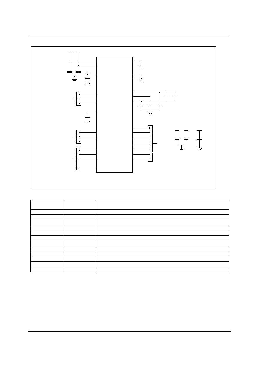
RECOMMENDED EXTERNAL COMPONENTS
3
10
1
28
27
7
5
6
12
11
9
4
DVDD1
DVDD2
AGND1
RINP
GINP
BINP
MCLK
VSMP
RLC/ACYC
SCK
SEN
SDI
OEB
8
26
24
25
23
20
19
18
17
16
15
14
13
OP[0]
OP[1]
OP[2]
OP[3]
OP[4]
OP[5]
OP[6]
OP[7]/SDO
VRLC/VBIAS
VRX
VRT
VRB
AVDD
C2
C1
C6
C8
C4
C5
C7
C9
AVDD
Video
Inputs
Timing
Signals
Interface
Controls
Output
Data
Bus
DGND
AGND
AGND
AGND
22
DGND
21
C3
AGND
AGND2
2
C11
C10
C12
AVDD
+
+
+
DGND
AGND
WM8196
C1-9 should be fitted as close to WM8196 as possible.
NOTES:
AGND and DGND should be connected as close to WM8196 as possible.
1.
2.
DVDD1 DVDD2
DVDD1 DVDD2
Figure 24 External Components Diagram
COMPONENT
REFERENCE
SUGGESTED
VALUE
DESCRIPTION
C1
100nF
De-coupling for DVDD1.
C2
100nF
De-coupling for DVDD2.
C3
100nF
De-coupling for AVDD.
C4
10nF
High frequency de-coupling between VRT and VRB.
C5
1
�
F
Low frequency de-coupling between VRT and VRB (non-polarised).
C6
100nF
De-coupling for VRB.
C7
100nF
De-coupling for VRX.
C8
100nF
De-coupling for VRT.
C9
100nF
De-coupling for VRLC.
C10
10
�
F
Reservoir capacitor for DVDD1.
C11
10
�
F
Reservoir capacitor for DVDD2.
C12
10
�
F
Reservoir capacitor for AVDD.
Table 7 External Components Descriptions

WM8196
Production Data
w
PD Rev 3.0 December 2002
27
PACKAGE DIMENSIONS
NOTES:
A. ALL LINEAR DIMENSIONS ARE IN MILLIMETERS.
B. THIS DRAWING IS SUBJECT TO CHANGE WITHOUT NOTICE.
C. BODY DIMENSIONS DO NOT INCLUDE MOLD FLASH ORPROTRUSION, NOT TO EXCEED 0.20MM.
D. MEETS JEDEC.95 MO-150, VARIATION = AH. REFER TO THIS SPECIFICATION FOR FURTHER DETAILS.
DM007.D
DS: 28 PIN SSOP (10.2 x 5.3 x 1.75 mm)
Symbols
Dimensions
(mm)
MIN
NOM
MAX
A
-----
-----
2.0
A
1
0.05
-----
0.25
A
2
1.65
1.75
1.85
b
0.22
0.30
0.38
c
0.09
-----
0.25
D
9.90
10.20
10.50
e
E
7.40
7.80
8.20
5.00
5.30
5.60
L
0.55
0.75
0.95
A A2
A1
14
1
15
28
E1
E
c
L
GAUGE
PLANE
0.25
e
b
D
SEATING PLANE
-C-
0.10 C
REF:
JEDEC.95, MO-150
E
1
L
1
0.125 REF
0.65 BSC
L
1
0
o
4
o
8
o

WM8196
Production Data
w
PD Rev 3.0 December 2002
28
IMPORTANT NOTICE
Wolfson Microelectronics plc (WM) reserve the right to make changes to their products or to discontinue any product or
service without notice, and advise customers to obtain the latest version of relevant information to verify, before placing
orders, that information being relied on is current. All products are sold subject to the WM terms and conditions of sale
supplied at the time of order acknowledgement, including those pertaining to warranty, patent infringement, and limitation
of liability.
WM warrants performance of its products to the specifications applicable at the time of sale in accordance with WM's
standard warranty. Testing and other quality control techniques are utilised to the extent WM deems necessary to support
this warranty. Specific testing of all parameters of each device is not necessarily performed, except those mandated by
government requirements.
In order to minimise risks associated with customer applications, adequate design and operating safeguards must be used
by the customer to minimise inherent or procedural hazards.
WM assumes no liability for applications assistance or customer product design. WM does not warrant or represent that
any license, either express or implied, is granted under any patent right, copyright, mask work right, or other intellectual
property right of WM covering or relating to any combination, machine, or process in which such products or services might
be or are used. WM's publication of information regarding any third party's products or services does not constitute WM's
approval, license, warranty or endorsement thereof.
Reproduction of information from the WM web site or datasheets is permissable only if reproduction is without alteration
and is accompanied by all associated warranties, conditions, limitations and notices. Representation or reproduction of this
information with alteration voids all warranties provided for an associated WM product or service, is an unfair and deceptive
business practice, and WM is not responsible nor liable for any such use.
Resale of WM's products or services with statements different from or beyond the parameters stated by WM for that
product or service voids all express and any implied warranties for the associated WM product or service, is an unfair and
deceptive business practice, and WM is not responsible nor liable for any such use.
ADDRESS:
Wolfson Microelectronics plc
20 Bernard Terrace
Edinburgh
EH8 9NX
United Kingdom
Tel :: +44 (0)131 272 7000
Fax :: +44 (0)131 272 7001
Email ::
sales@wolfsonmicro.com