
WM8199
20MSPS 16-bit CCD Digitiser
WOLFSON MICROELECTRONICS plc
w :: www.wolfsonmicro.com
Production Data, November 2003, Rev 3.2
Copyright
2003 Wolfson Microelectronics plc
DESCRIPTION
The WM8199 is a 16-bit analogue front end/digitiser IC
which processes and digitises the analogue output signals
from CCD sensors or Contact Image Sensors (CIS) at pixel
sample rates of up to 20MSPS.
The device includes three analogue signal processing
channels each of which contains Reset Level Clamping,
Correlated Double Sampling and Programmable Gain and
Offset adjust functions. Three multiplexers allow single
channel processing. The output from each of these
channels is time multiplexed into a single high-speed 16-bit
Analogue to Digital Converter. The digital output data is
available in 8 or 4-bit wide multiplexed format.
An internal 4-bit DAC is supplied for internal reference level
generation. This may be used during CDS to reference CIS
signals or during Reset Level Clamping to clamp CCD
signals. An external reference level may also be supplied.
ADC references are generated internally, ensuring optimum
performance from the device.
Using an analogue supply voltage of 5V and a digital
interface supply of either 5V or 3.3V, the WM8199 typically
only consumes 358mW when operating from a single
5V supply.
FEATURES
∑
16-bit ADC
∑
20MSPS conversion rate
∑
30MSPS conversion rate at 8-bits
∑
Low power ≠ 358mW typical
∑
5V single supply or 5V/3.3V dual supply operation
∑
Single or 3 channel operation
∑
Correlated double sampling
∑
Programmable gain (8-bit resolution)
∑
Programmable offset adjust (8-bit resolution)
∑
Programmable clamp voltage
∑
8 or 4-bit wide multiplexed data output formats
∑
Internally generated voltage references
∑
28-pin SSOP package
∑
Serial control interface
APPLICATIONS
∑
Flatbed and sheetfeed scanners
∑
USB compatible scanners
∑
Multi-function peripherals
∑
High-performance CCD sensor interface
BLOCK DIAGRAM
RINP
DATA
I/O
PORT
SEN
VSMP
MCLK
VRLC/VBIAS
SDI
SCK
DVDD2
TIMING CONTROL
CL
RLC/ACYC
RLC
V
S
R
S
BINP
GINP
VRX
VRT
OEB
M
U
X
VRB
RLC
RLC
CDS
CDS
CDS
RLC
DAC
4
CONFIGURABLE
SERIAL
CONTROL
INTERFACE
16-
BIT
ADC
AGND1
DGND
DVDD1
OP[0]
OP[1]
OP[2]
OP[3]
OP[4]
OP[5]
OP[6]
OP[7]/SDO
AGND2
M
U
X
VREF/BIAS
M
U
X
R
G
B
M
U
X
R
G
B
+
PGA
I/P SIGNAL
POLARITY
ADJUST
8
8
PGA
8
8
OFFSET
DAC
PGA
8
OFFSET
DAC
8
+
+
+
+
+
I/P SIGNAL
POLARITY
ADJUST
I/P SIGNAL
POLARITY
ADJUST
AVDD
w
WM8199
OFFSET
DAC

WM8199
Production Data
w
PD Rev 3.2 November 2003
2
TABLE OF CONTENTS
DESCRIPTION .......................................................................................................1
FEATURES.............................................................................................................1
APPLICATIONS .....................................................................................................1
BLOCK DIAGRAM .................................................................................................1
TABLE OF CONTENTS .........................................................................................2
PIN CONFIGURATION...........................................................................................3
ORDERING INFORMATION ..................................................................................3
ABSOLUTE MAXIMUM RATINGS .........................................................................5
RECOMMENDED OPERATING CONDITIONS .....................................................5
ELECTRICAL CHARACTERISTICS ......................................................................6
TYPICAL HIGH SPEED PERFORMANCE..................................................................... 8
INPUT VIDEO SAMPLING ............................................................................................. 9
OUTPUT DATA TIMING ................................................................................................ 9
SERIAL INTERFACE ................................................................................................... 10
DEVICE DESCRIPTION .......................................................................................12
INTRODUCTION.......................................................................................................... 12
INPUT SAMPLING ....................................................................................................... 12
RESET LEVEL CLAMPING (RLC) ............................................................................... 12
CDS/NON-CDS PROCESSING ................................................................................... 13
OFFSET ADJUST AND PROGRAMMABLE GAIN ....................................................... 14
ADC INPUT BLACK LEVEL ADJUST .......................................................................... 14
OVERALL SIGNAL FLOW SUMMARY ........................................................................ 15
CALCULATING OUTPUT FOR ANY GIVEN INPUT .................................................... 15
OUTPUT FORMATS .................................................................................................... 16
CONTROL INTERFACE .............................................................................................. 17
TIMING REQUIREMENTS ........................................................................................... 17
PROGRAMMABLE VSMP DETECT CIRCUIT ............................................................. 18
REFERENCES............................................................................................................. 18
POWER SUPPLY ........................................................................................................ 18
POWER MANAGEMENT ............................................................................................. 19
LINE-BY-LINE OPERATION ........................................................................................ 19
OPERATING MODES .................................................................................................. 20
OPERATING MODE TIMING DIAGRAMS ................................................................... 21
DEVICE CONFIGURATION .................................................................................24
REGISTER MAP .......................................................................................................... 24
REGISTER MAP DESCRIPTION ................................................................................. 25
RECOMMENDED EXTERNAL COMPONENTS ..................................................28
PACKAGE DIMENSIONS ....................................................................................29
IMPORTANT NOTICE ..........................................................................................30
ADDRESS:................................................................................................................... 30
WM8199
Production Data
w
PD Rev 3.2 November 2003
3
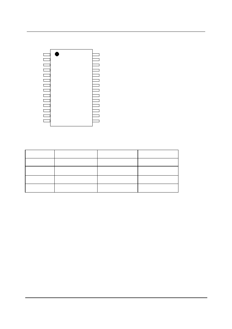
PIN CONFIGURATION
SEN
OP[1]
OP[0]
SCK
SDI
DVDD2
OP[7]/SDO
OP[2]
OP[3]
OP[4]
OP[5]
OP[6]
GINP
AGND1
VRB
VRT
VRX
VRLC/VBIAS
BINP
AVDD
DGND
AGND2
DVDD1
OEB
VSMP
RLC/ACYC
MCLK
RINP
1
2
3
4
5
6
7
8
9
10
11
12
13
14
28
27
26
25
24
23
22
21
20
19
18
17
16
15
ORDERING INFORMATION
DEVICE
TEMP. RANGE
PACKAGE
MOISTURE SENSITIVITY
LEVEL
WM8199CDS
0 to 70
o
C
28-pin SSOP
MSL1
WM8199CDS/R
0 to 70
o
C
28-pin SSOP
(tape and reel)
MSL1
WM8199SCDS
0 to 70
o
C
28-pin SSOP
(lead free)
MSL1
WM8199SCDS/R
0 to 70
o
C
28-pin SSOP
(lead free, tape and reel)
MSL1
Note:
Reel quantity = 2,000
WM8199
Production Data
w
PD Rev 3.2 November 2003
4
PIN DESCRIPTION
PIN
NAME
TYPE
DESCRIPTION
1
RINP
Analogue input
Red channel input video.
2
AGND2
Supply
Analogue ground (0V).
3
DVDD1
Supply
Digital supply (5V) for logic and clock generator. This must be operated at the same
potential as AVDD.
4
OEB
Digital input
Output Hi-Z control, all digital outputs disabled when OEB = 1.
5
VSMP
Digital input
Video sample synchronisation pulse.
6
RLC/ACYC
Digital input
RLC (active high) selects reset level clamp on a pixel-by-pixel basis ≠ tie high if
used on every pixel. ACYC autocycles between R, G, B inputs.
7
MCLK
Digital input
Master clock. This clock is applied at N times the input pixel rate (N = 2, 3, 6, 8 or
any multiple of 2 thereafter depending on input sample mode).
8
DGND
Supply
Digital ground (0V).
9
SEN
Digital input
Enables the serial interface when high.
10
DVDD2
Supply
Digital supply (5V/3.3V), all digital I/O pins.
11
SDI
Digital input
Serial data input.
12
SCK
Digital input
Serial clock.
Digital multiplexed output data bus.
ADC output data (d15:d0) is available in two multiplexed formats as shown, under
the control of register MUXOP [1:0]
See `Output Formats' description in Device Description section for further details.
8+8-bit
4+4+4+4-bit
A
B
A
B
C
D
13
OP[0]
Dig ital output
d8
d0
14
OP[1]
Dig ital output
d9
d1
15
OP[2]
Digital output
d10
d2
16
OP[3]
Digital output
d11
d3
17
OP[4]
Digital output
d12
d4
d12
d8
d4
d0
18
OP[5]
Digital output
d13
d5
d13
d9
d5
d1
19
OP[6]
Digital output
d14
d6
d14
d10
d6
d2
20
OP[7]/SDO
Digital output
d15
d7
d15
d11
d7
d3
Alternatively, pin OP[7]/SDO may be used to output register read-back data when
OEB = 0 and SEN has been pulsed high. See Serial Interface description in Device
Description section for further details.
21
AVDD
Supply
Analogue supply (5V). This must be operated at the same potential as DVDD1.
22
AGND1
Supply
Analogue ground (0V).
23
VRB
Analogue output
Lower reference voltage.
This pin must be connected to AGND via a decoupling capacitor.
24
VRT
Analogue output
Upper reference voltage.
This pin must be connected to AGND via a decoupling capacitor.
25
VRX
Analogue output
Input return bias voltage.
This pin must be connected to AGND via a decoupling capacitor.
26
VRLC/VBIAS
Analogue I/O
Selectable analogue output voltage for RLC or single-ended bias reference.
This pin would typically be connected to AGND via a decoupling capacitor.
VRLC can be externally driven if programmed Hi-Z.
27
BINP
Analogue input
Blue channel input video.
28
GINP
Analogue input
Green channel input video.
WM8199
Production Data
w
PD Rev 3.2 November 2003
5
ABSOLUTE MAXIMUM RATINGS
Absolute Maximum Ratings are stress ratings only. Permanent damage to the device may be caused by continuously operating at
or beyond these limits. Device functional operating limits and guaranteed performance specifications are given under Electrical
Characteristics at the test conditions specified.
ESD Sensitive Device. This device is manufactured on a CMOS process. It is therefore generically susceptible
to damage from excessive static voltages. Proper ESD precautions must be taken during handling and storage
of this device.
Wolfson tests its package types according to IPC/JEDEC J-STD-020B for Moisture Sensitivity to determine acceptable storage
conditions prior to surface mount assembly. These levels are:
MSL1 = unlimited floor life at <30
∞
C / 85% Relative Humidity. Not normally stored in moisture barrier bag.
MSL2 = out of bag storage for 1 year at <30
∞
C / 60% Relative Humidity. Supplied in moisture barrier bag.
MSL3 = out of bag storage for 168 hours at <30
∞
C / 60% Relative Humidity. Supplied in moisture barrier bag.
The Moisture Sensitivity Level for each package type is specified in Ordering Information.
CONDITION
MIN
MAX
Analogue supply voltage: AVDD
GND - 0.3V
GND + 7V
Digital supply voltages: DVDD1
-
2
GND - 0.3V
GND + 7V
Digital ground: DGND
GND - 0.3V
GND + 0.3V
Analogue grounds: AGND1
-
2
GND - 0.3V
GND + 0.3V
Digital inputs, digital outputs and digital I/O pins
GND - 0.3V
DVDD2 + 0.3V
Analogue inputs (RINP, GINP, BINP)
GND - 0.3V
AVDD + 0.3V
Other pins
GND - 0.3V
AVDD + 0.3V
Operating temperature range: T
A
0
∞
C
+70
∞
C
Storage temperature after soldering
-65
∞
C
+150
∞
C
Package body temperature (soldering, 10 seconds)
+260
∞
C
Package body temperature (soldering, 2 minutes)
+183
∞
C
Notes:
1.
GND denotes the voltage of any ground pin.
2.
AGND1, AGND2 and DGND pins are intended to be operated at the same potential. Differential voltages
between these pins will degrade performance.
RECOMMENDED OPERATING CONDITIONS
CONDITION
SYMBOL
MIN
TYP
MAX
UNITS
Operating temperature range
T
A
0
70
∞
C
Analogue supply voltage
AVDD
4.75
5.0
5.25
V
Digital core supply voltage
DVDD1
4.75
5.0
5.25
V
5V I/O
DVDD2
4.75
5.0
5.25
V
Digital I/O supply voltage
3.3V I/O
DVDD2
2.97
3.3
3.63
V