Document Outline
- WM8200-10/12
- DESCRIPTION
- FEATURES
- APPLICATIONS
- BLOCK DIAGRAM
- PIN CONFIGURATION
- ORDERING INFORMATION
- PIN DESCRIPTION
- ABSOLUTE MAXIMUM RATINGS
- RECOMMENDED OPERATING CONDITIONS
- ELECTRICAL CHARACTERISTICS
- DEVICE DESCRIPTION
- INTRODUCTION
- ANALOGUE SIGNAL PATH
- ADC REFERENCE MODES
- DC CLAMP
- COARSE OFFSET
- CONTROL INTERFACE
- REGISTER MAP
- REGISTER MAP DESCRIPTION
- POWER MANAGEMENT
- DATA OUTPUT FORMAT
- REFERENCE VOLTAGE GENERATION
- REFERENCE DECOUPLING
- PACKAGE DIMENSIONS
- IMPORTANT NOTICE
- ADDRESS
w
WM8200-10/12
40MSPS ADC with PGA
WOLFSON MICROELECTRONICS LTD
www.wolfsonmicro.com
Product Preview March 2002, Rev 1.22
Copyright
2002 Wolfson Microelectronics Ltd.
DESCRIPTION
The WM8200 is a CMOS high speed, low power, pipeline
analogue-to-digital converter (ADC) with 10 or 12-bit output
options. It also has an on-chip programmable gain amplifier
(PGA), dc clamp circuit and internal voltage references.
Conversion is controlled by a single clock input.
The device has a high bandwidth differential sample and hold
input, which gives excellent common-mode noise immunity
and low distortion. Alternatively, it can be driven in single
ended fashion with an optional voltage clamp for dc
restoration that can take its reference from an on-chip 10-bit
DAC.
The WM8200 provides internal reference voltages for setting
the ADC full-scale range without the requirement for external
circuitry. However, it can also accept external references for
applications where shared or high-precision references are
required.
A 3-wire serial interface is used to control the device and a
10 or 12-bit parallel interface is to read ADC conversion data.
ADC data can be output in unsigned binary or two's
complement format.
The WM8200 operates with a single 3V supply and is
supplied in a 28-lead QFN package.
FEATURES
�
10 or 12-bit resolution ADC
�
40MSPS
conversion
rate
�
Programmable Gain Amplifier (PGA)
�
Adjustable internal voltage references
�
Built in clamp function (dc restore) with 10-bit DAC
�
Wide Input Bandwidth - 900MHz
�
Unsigned Binary or Two's complement output format
�
Programmable via 3-wire serial MPU interface
�
Single 3V supply operation
�
Low power - 100mW typical at 3.0V supplies
�
Powerdown mode to <0.1mW typical
�
28 lead QFN package
APPLICATIONS
�
Digital
Still
Cameras
�
Composite
Video
Digitisation
�
Digital
Copiers
�
Digital Video Cameras
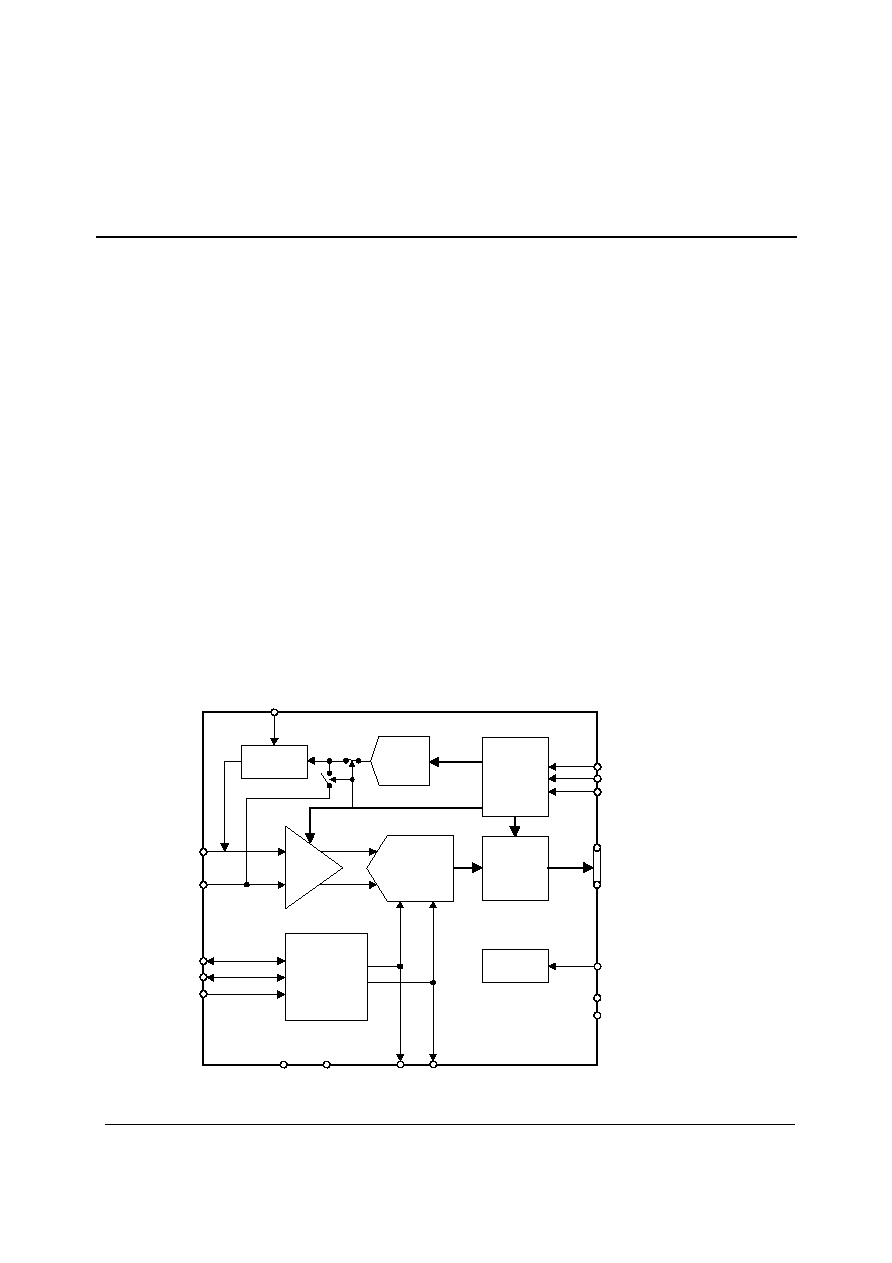
BLOCK DIAGRAM
AINP
ON-CHIP
REFERENCE
GENERATOR
ADC
Core
S/H
PGA
AINN
DO[9:0] WM8200-10
or
DO[11:0] WM8200-12
OUTPUT
BUFFERS
MODE
REFSENSE
AGND
AVDD
REFB
REFT
DGND
DVDD
SDIN
TIMING
CONTROL
CLK
VREF
WM8200
CSB
SCLK
CLAMP
AMPLIFIER
CLAMP
REGISTERS
CONTROL
CLAMP
LEVEL
DAC
ADC
CORE
WM8200
Product Preview
w
PP Rev 1.22 March 2002
2
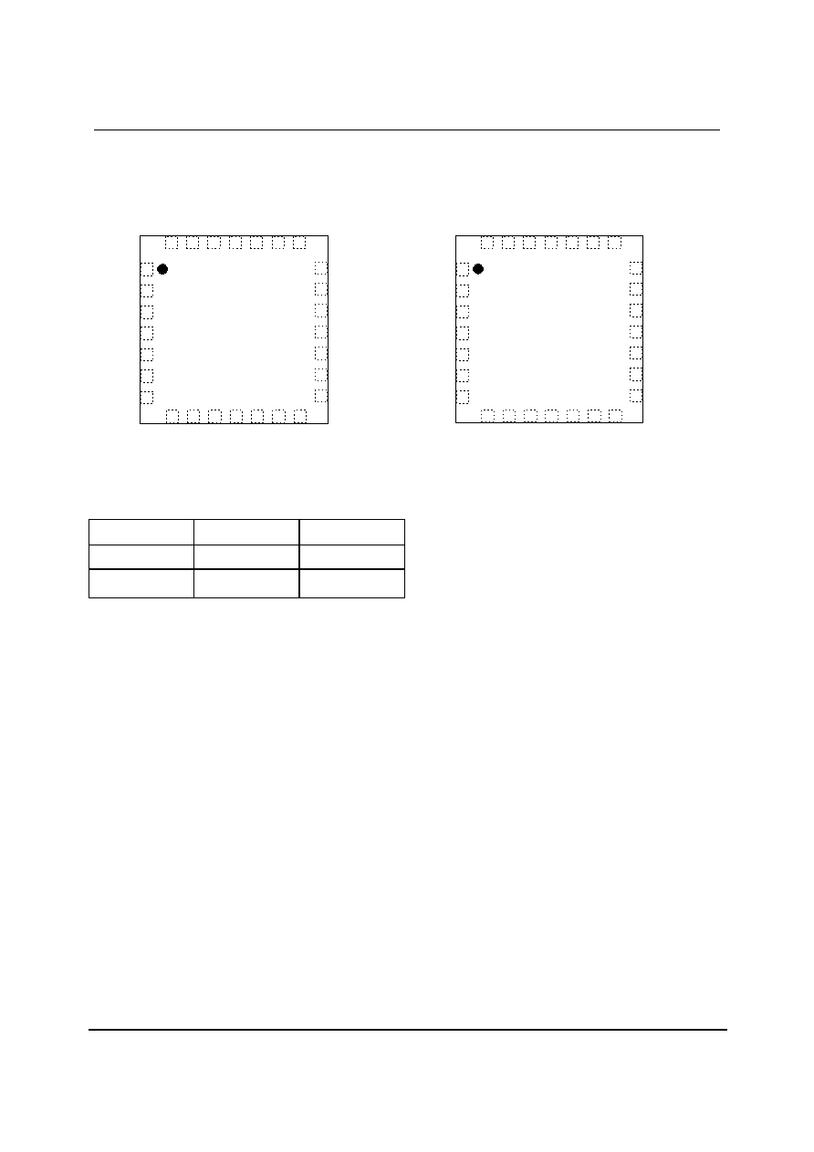
PIN CONFIGURATION
WM8200-10
AINP
AINN
REFB
MODE
REFT
CLAMP
REFSENSE
DO
8
DO
9
SC
LK
DG
ND
CL
K
CS
B
SD
I
N
DO1
DO2
DO3
DO4
DO5
DO6
DO7
DO
0
NC
NC
DV
DD
AGN
D
AVD
D
VR
EF
7
6
5
4
3
2
1
8
9
10
11
13
12
14
17
18
21
20
19
15
16
28
27 26
25
24
23
22
WM8200-12
AINP
AINN
REFB
MODE
REFT
CLAMP
REFSENSE
DO
1
0
DO
1
1
SC
LK
DG
ND
CL
K
CS
B
SD
I
N
DO3
DO4
DO5
DO6
DO7
DO8
DO9
DO
2
DO
1
DO
0
DV
D
D
AGN
D
AVD
D
VR
EF
7
6
5
4
3
2
1
8
9
10
11
13
12
14
17
18
21
20
19
15
16
28
27 26
25
24
23
22
ORDERING INFORMATION
DEVICE TEMP.
RANGE
PACKAGE
WM8200-10IFL
-40 to +85
o
C
28-lead QFN
WM8200-12IFL
-40 to +85
o
C
28-lead QFN

WM8200
Product Preview
w
PP Rev 1.22 March 2002
3
PIN DESCRIPTION
PIN
NAME
TYPE
DESCRIPTION
1 DO1
DO3 Digital
Output Digital output bit
2 DO2
DO4 Digital
Output Digital output bit
3 DO3
DO5 Digital
Output Digital output bit
4 DO4
DO6 Digital
Output Digital output bit
5 DO5
DO7 Digital
Output Digital output bit
6 DO6
DO8 Digital
Output Digital output bit
7 DO7
DO9 Digital
Output Digital output bit
8 DO8
DO10 Digital
Output Digital output bit
9 DO9
DO11 Digital
Output Digital output bit (MSB)
10 SCLK Digital
Input
3-Wire Control Interface Clock Input
11 DGND
Ground Negative Digital Supply
12 CLK Analogue
Input
Clock input
13 CSB Digital
Input
3-Wire Control Interface Chip Select
14
SDIN
Digital Input
3-Wire Control Interface Data Input
15 REFSENSE Analogue
Input VREF feedback/configuration control
16 CLAMP Digital
Input High to enable clamp mode, low to disable clamp mode
17 REFT
Analogue
Input/Output
Top ADC reference voltage
18 MODE Analogue
Input
High (MODE=AVDD) to enable internal ADC references.
Low (MODE=AVSS) to enable use of external ADC references applied to
REFT and REFB.
19 REFB
Analogue
Input/Output
Bottom ADC reference voltage
20 AINN Analogue
Input
Positive analogue input
21 AINP Analogue
Input
Negative analogue Input
22
VREF
Analogue Input/Output
Internal/external reference voltage
23 AVDD
Supply Positive Analogue Supply
24 AGND
Ground Negative Analogue Supply
25 DVDD
Supply Positive Digital Supply
26 NC
DO0 Digital
Output Not internally connected (10-bit option)/
Digital output bit (LSB for 12-bit option only)
27 NC
DO1 Digital
Output Not internally connected (10-bit option) /
Digital output bit (for 12-bit Option Only)
28 DO0
DO2 Digital
Output
Digital output bit (LSB for 10-bit Option)
WM8200
Product Preview
w
PP Rev 1.22 March 2002
4
ABSOLUTE MAXIMUM RATINGS
Absolute Maximum Ratings are stress ratings only. Permanent damage to the device may be caused by continuously operating at
or beyond these limits. Device functional operating limits and guaranteed performance specifications are given under Electrical
Characteristics at the test conditions specified.
ESD Sensitive Device. This device is manufactured on a CMOS process. It is therefore generically susceptible
to damage from excessive static voltages. Proper ESD precautions must be taken during handling and storage
of this device.
CONDITION
MIN MAX
Digital supply voltage, DVDD to DGND
-0.3V +3.63V
Analog supply voltage, AVDD to AGND
-0.3V +3.63V
Maximum voltage difference between AGND and DGND
-0.3V +0.3V
Voltage range digital input (SCLK, SDIN, CSB, CLAMP)
DGND - 0.3V
DVDD + 0.3V
Voltage range analog inputs
AGND - 0.3V
AVDD + 0.3V
Voltage range CLK, MODE inputs
AGND - 0.3V
AVDD + 0.3V
Operating junction temperature range, T
J
-40
�
C +150
�
C
Storage temperature
-65
�
C +150
�
C
Package Body Temperature (soldering 10 seconds)
+240
�
C
Package Body Temperature (soldering 2 minutes)
+183
�
C
RECOMMENDED OPERATING CONDITIONS
PARAMETER SYMBOL
TEST
CONDITIONS
MIN
NOM
MAX
UNIT
Digital supply range
DVDD
3.0 3.3 3.6 V
Analog supply range
AVDD
3.0
3.3
3.6 V
Ground
DGND, AGND
0
V
Clock frequency
f
CLK
5
40
MHz
Clock duty cycle
45
50
55
%
Operating Free Air Temperature
T
A
-40
85
�
C

WM8200
Product Preview
w
PP Rev 1.22 March 2002
5
ELECTRICAL CHARACTERISTICS
Test Conditions:
AVDD = DVDD = 3.0V, f
CLK
= 40MHz, 50% duty cycle, MODE = AVDD, VREF=1.0V (REFT = 2.0V, REFB = 1.0V),
PGA gain = 1.0, T
A
= T
MIN
to T
MAX
, unless otherwise stated.
PARAMETER SYMBOL
TEST
CONDITIONS
MIN
TYP
MAX
UNIT
DC Accuracy
Integral nonlinearity
INL
�
1.0 LSB
Differential nonlinearity
DNL
�
0.3 LSB
Offset error
0.7
%
of
FSR
Full scale error
2.2
%
of
FSR
Missing codes
No missing codes guaranteed
Analogue Input Signal to AIN pins
Differential analogue input
voltage (AINP-AINN)
PGA=1x
gain
-1 1 V
Switched input capacitance
1.2 pF
Conversion Characteristics
Conversion frequency
f
CLK
5
40
MHz
Pipeline delay
4
cycles of
CLK
Dynamic Performance (differential input mode)
f
IN
=
4.8MHz 9.6
Effective number of bits
ENOB
f
IN
=
20MHz 9.5
bits
f
IN
= 4.8MHz
72
Spurious free dynamic range
SFDR
f
IN
= 20MHz
70
dB
f
IN
= 4.8MHz
-72.5
Total harmonic distortion
THD
f
IN
= 20MHz
-71.6
dB
f
IN
= 4.8MHz
60
Signal to noise ratio
SNR
f
IN
= 20MHz
57
dB
f
IN
= 4.8MHz
59.7
Signal to noise and distortion
ratio
SINAD
f
IN
= 20MHz
59.6
dB
PGA
Gain range (linear scale)
0.5
4
V/V
Gain step size (linear scale)
0.5 V/V
Clamp
Clamp DAC resolution
10
bits
Clamp DAC output voltage
REFB REFT V
Clamp DAC DNL
�1
LSB
Clamp output voltage error
-40
40
mV
REFB, REFT internal ADC reference voltage outputs (MODE= AVDD)
VREF = 0.5V
1.75
Reference voltage top, REFT
(AVDD=3V)
VREF= 1.0V
2
VREF = 0.5V
1.25
Reference voltage bottom,
REFB (AVDD=3V)
VREF= 1.0V
1
VREF Input / Output specifications (ADC Input Range = VREFx2)
Internal 0.5V reference to VREF
REFSENSE
=
VREF
0.5 V
Internal 1V reference to VREF
REFSENSE
=
AGND
1
V
External reference applied to
VREF pin
REFSENSE
=
AVDD
0.5
1
V
Input impedance in internal ADC
reference mode
REFSENSE = AVDD,
MODE = AVDD
14 k
WM8200
Product Preview
w
PP Rev 1.22 March 2002
6
Test Conditions:
AVDD = DVDD = 3.0V, f
CLK
= 40MHz, 50% duty cycle, MODE = AVDD, VREF=1.0V (REFT = 2.0V, REFB = 1.0V),
PGA gain = 1.0, T
A
= T
MIN
to T
MAX
, unless otherwise stated.
PARAMETER SYMBOL
TEST
CONDITIONS
MIN
TYP
MAX
UNIT
Power Supplies
MODE = AGND
28.5
mA
Analogue supply current
I
AVDD
MODE = AVDD
31
mA
Digital supply current
I
DVDD
C
L
= 10pF
5
mA
Standby power consumption
(digital and analogue combined)
I
VDD
(STBY)
75
uW
Digital Logic Levels (CMOS Levels)
Input LOW level
V
IL
(Note 1)
0.2 x VDD
V
Input HIGH level
V
IH
(Note 1)
0.8 x VDD
V
Output LOW
V
OL
I
OL
= -50
�
A 0.4
V
Output HIGH
V
OH
I
OH
= 50
�
A VDD
�
0.4
V
Notes
1.
Digital input and output levels refer to the supply used for the input/output buffer on the relevant pin. CLK and MODE
refer to the AVDD supply, all other digital input/output refers to the DVDD supply.
CONTROL INTERFACE TIMING
CSB
SCLK
SDIN
t
CSL
t
DHO
t
DSU
t
CSH
t
SCY
t
SCH
t
SCL
t
SCS
LSB
t
CSS
Figure 1: Control Interface Timing
Test Conditions
AVDD = DVDD = 3.0V, AGND = DGND = 0V, T
A
= T
MIN
to T
MAX
, unless otherwise stated
PARAMETER SYMBOL
TEST
CONDITIONS
MIN
TYP
MAX
UNIT
Program Register Input Information
SCLK rising edge to CSB rising
edge
t
SCS
60
ns
SCLK pulse cycle time
t
SCY
80
ns
SCLK pulse width low
t
SCL
30
ns
SCLK pulse width high
t
SCH
30
ns
SDIN to SCLK set-up time
t
DSU
20
ns
SCLK to SDIN hold time
t
DHO
20
ns
CSB pulse width low
t
CSL
20
ns
CSB pulse width high
t
CSH
20
ns
CSB rising to SCLK rising
t
CSS
20
ns
Table 1 Control Interface Timing Information
WM8200
Product Preview
w
PP Rev 1.22 March 2002
7
DEVICE DESCRIPTION
INTRODUCTION
The WM8200 is a high speed analogue to digital converter (ADC) with on-chip analogue pre-
processing and reference generation, deisgned for applications such as composite video digitisation
digital copiers and high speed data acquisition. The integrated clamp and the coarse offset function
mean the device is ideally suited to CCD/CMOS input systems such as colour scanners, digital
copiers and digital cameras. A wide input voltage range between REFB and REFT allows the
WM8200 to be used in both imaging and communications systems.The chip architecture consists of:
�
High bandwidth sample and hold input, which can operate in differential or single-
ended mode
�
Programmable gain amplifier (PGA)
�
Voltage clamp for DC restoration that can take its reference from an on-chip 10-bit
DAC or an external source
�
Coarse offset function to allow clamping with single ended CCD style inputs
�
10-bit,
40MSPS
pipeline
analogue-to-digital converter (ADC) core
�
On-chip reference generator and reference buffer (external references can also be
used for applications where common or high precision references are required)
�
10-bit parallel output for ADC conversion. ADC data can be output in unsigned binary
or two's complement format. An out-of-range output pin indicates when the input signal
is outside the converter's range
�
Serial control interface to configure the operation of the device.
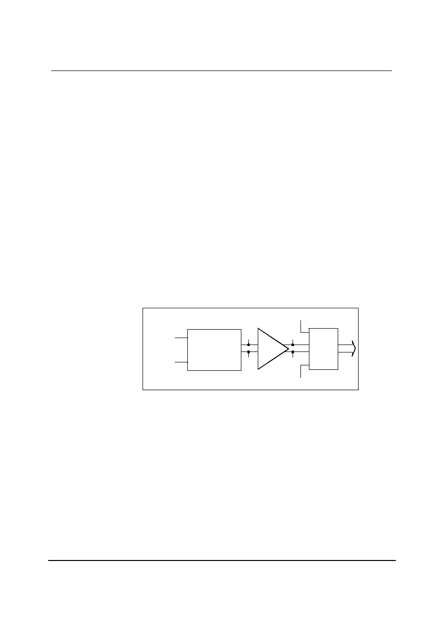
ANALOGUE SIGNAL PATH
The WM8200 analogue signal path consists of a DC clamp with a 10-bit clamp level DAC (discussed
under `DC Clamp', below), a high-bandwidth sample and hold unit followed by a programmable gain
amplifier (PGA) and a fast 10-bit pipelined analogue to digital converter (ADC core).
Figure 2 Analogue Input Signal Flow
Figure 2 shows the signal flow through the sample and hold unit and the PGA to the ADC core,
where the process of analogue to digital conversion is performed against the ADC reference
voltages, REFT and REFB (their generation from internal or external reference sources is described
later).
SAMPLE AND HOLD
The differential analogue input signals can be connected directly to the AINN and AINP pins, either
DC coupled, AC coupled, or AC coupled with DC restoration using the WM8200 clamp circuit.
The differential sample and hold processes V
INP
and V
INN
with respect to the voltages applied to the
REFT and REFB pins, and produces a differential output V
P
= V
P+
- V
P-
given by:
AINN
AINP
V
P
-
=
For single-ended input signals, the signal can be DC or AC coupled to either AINN or AINNP, and a
suitable reference voltage must be applied to the other pin. Note of the input signal is applied to
AINN this will result in it being inverted during sampling.
SAMPLE
AND
HOLD
AINN
AINP
X-1
X
PGA
VP+
VP-
REFT
REFB
ADC
CORE
VQ+
VQ-

WM8200
Product Preview
w
PP Rev 1.22 March 2002
8
(
)
(
)
(
)
(
)
Gain
REFB
REFT
]
AINN
AINP
[
Gain
REFT
REFB
�
-
-
�
-
2
2
PROGRAMMABLE-GAIN AMPLIFIER
V
P
is amplified by the PGA and fed into the ADC as a differential voltage V
Q
= V
Q+
- V
Q-
(
)
INN
INP
P
Q
V
V
Gain
V
Gain
V
-
�
=
�
=
The PGA gain defaults to 1.0 at power-up, but can be programmed from 0.5 to 4.0 in steps of 0.5.
ANALOGUE-TO-DIGITAL CONVERTER
Regardless of the reference configuration, V
Q
is digitised against ADC Reference voltages REFT and
REFB, full scale values of V
Q
being given by:
2
REFB
REFT
V
QFS
-
=
-
-
=
2
REFB
REFT
V
QZS
Attempts to convert V
Q
voltages outside the range of V
QZS
to V
QFS
are signalled to the application by
driving the OVR output pin high when the conversion result is output. If V
Q
is less than V
QZS
, the ADC
output code is 0. If V
Q
is greater than V
QFS
, the output code is 1023.
SIGNAL CHAIN SUMMARY
Combining the above equations to find the input voltages [AINP � AINN] that correspond to the limits
of the ADCs valid input range gives:
Therefore the input signal span is given by:
Gain
REFB
REFT
AINN
AINP
-
=
-
In order to match the ADC input range to the input signal amplitude, REFT and REFB should be set
such that:
Gain
)
AINN
AINP
(
REFB
REFT
�
-
=
-
ADC REFERENCE MODES
The WM8200 references REFT and REFB can be driven from external (off-chip) sources or from the
internal reference generation/buffer circuit. The mode of operation is selected by the voltage applied
to the MODE pin. These are summarised and explained in Table 2.
Note that the internally generated ADC references are intended solely for WM8200 internal use and
REFT and REFB must not be used as voltage references for any other device in the application.
MODE
PIN
MODE FUNCTION
COMMENTS
AGND Full
external
external
REFT
=
external
REFB
=
On-chip reference generator and reference buffer are
not used.
AVDD Top/Bottom
(
)
2
REFBS
REFTS
AVDD
REFTF
-
+
=
(
)
2
REFBS
REFTS
AVDD
REFBF
-
-
=
On-chip reference generator is not used. Reference
buffer centers external reference voltages around
AVDD/2.
Table 2 WM8200 Reference Generation Modes
and zero scale by
WM8200
Product Preview
w
PP Rev 1.22 March 2002
9
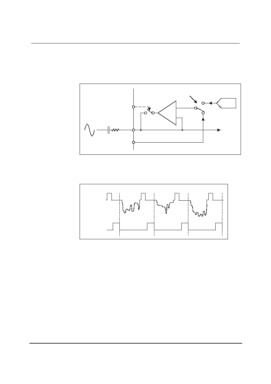
DC CLAMP
The WM8200 incorporates a clamp function for restoring the DC reference level of AC coupled input
signals. When the clamp input pin is held high the internal clamp amplifier forces the voltage at
AINP to equal the clamp reference voltage, setting the DC level at AINP.
The clamp reference voltage comes from the on-chip 10-bit Clamp Level DAC by default, however it
can be applied to the AINN pin if the CLPSEL register bit is set high.
CLAMP
AINN
-
+
AINP
10-Bit DAC
SW1
Control
Register
S/H
R
IN
C
IN
Vclamp
Figure 3 Schematic of Clamp Circuitry
Figure 4 shows an example of using the clamp to restore the black level of a composite video input
AC coupled to AINN. While the clamp pin is held high, the clamp amplifier forces the voltage at AINN
to equal the clamp reference voltage, setting the DC voltage at AINN for the video black level.
VIDEO AT
AINN
CLAMP
Line sync
Black
level
Figure 4 Example Waveforms for Line-Clamping to a Video Input Black Level
If the CLAMP amplifier is not required it can be disabled for power saving purposes by setting the
CLPDIS register bit to high.
CLAMP DAC OUTPUT VOLTAGE RANGE AND LIMITS
Important: When using the internal clamp DAC in Top/Bottom or Centre Span Mode, the user must
ensure that the desired DC clamp level at AIN lies within the voltage range REFB to REFT. This is
because the clamp DAC voltage is constrained to lie within this range REFB to REFT. Specifically:
V
DAC
= REFB + (REFT � REFB) x (0.006 +0.988 x (DAC_code)/1024)
DAC codes can range from 0 to 1023. Figure 5 shows the clamp DAC output voltage versus the
DAC code.

WM8200
Product Preview
w
PP Rev 1.22 March 2002
10
VDAC
DAC
code
0
1023
VREFBF + 0.987(VREFTF-VREFBF)
VREFBF
VREFTF
VREFBF + 0.006(VREFTF-VREFBF)
Figure 5 Clamp DAC Output Voltage versus DAC Register Code Value
COARSE OFFSET
The WM8200 features a coarse offset feature which allows it to accommodate both positive-going
and negative-going input signals when using the DC clamp. This feature is enabled by setting the
PGAOFF register bit to high.
DIAGRAM SHOWING COARSE OFFSET TO BE INSERTED

WM8200
Product Preview
w
PP Rev 1.22 March 2002
11
CONTROL INTERFACE
The internal control registers are programmable via the 3-wire serial interface. SDIN is used for the
program data, SCLK is used to clock in the data and CSB is used to latch in the program data. The
3-wire interface protocol is shown in Figure 6.
Figure 6: 3-Wire Serial Interface
1.
A[3:0] are Control Address Bits
2.
D[7:0] are Control Data Bits
3.
CSB is edge sensitive � the data is latched on the rising edge of CSB.
REGISTER MAP
Table 3 shows the location of each control bit used to determine the operation of the WM8200. The
procedure for programming the register map is described in the CONTROL INTERFACE section.
BIT
ADDR
NAME DEFAULT
(HEX)
B7 B6 B5 B4 B3
B2 B1 B0
0000 Clamp
Reg
1
00
DAC[7] DAC[6] DAC[5] DAC[4] DAC[3]
DAC[2] DAC[1] DAC[0]
0001
Clamp Reg 2
00
0
0
0 0 0 0
DAC[9]
DAC[8]
0010
PGA Control
01
0
0
PGASENSE
PGAOFF
0 PGA[2]
PGA[1]
PGA[0]
0011
Control
00
0
0
0 CLPSEL
OEB TWOSC CLDIS
PD
0100 -
1111
Reserved
00
Reserved, do not write to these register locations
Table 3: Register Map
D7 D6 D5 D4 D3 D2 D1 D0
CSB
SCLK
SDIN
A3 A2 A1 A0
ADDRESS
DATA

WM8200
Product Preview
w
PP Rev 1.22 March 2002
12
REGISTER MAP DESCRIPTION
REGISTER
BIT BIT
NAMES
DEFAULT
DESCRIPTION
Clamp
Register 1
7:0 DAC[7:0]
00000000
Clamp DAC value bits 7 to 0 (Unsigned binary format)
Clamp
Register 2
1:0 DAC[9:8] 00 Clamp DAC value bits 9 to 8 (Unsigned binary format)
PGA Gain control
000: PGA Gain = 0.5x
100: PGA Gain = 2.5x
001: PGA Gain = 1.0x
101: PGA Gain = 3.0x
010: PGA Gain = 1.5x
110: PGA Gain = 3.5x
2:0 PGA[2:0] 001
011: PGA Gain = 2.0x
111: PGA Gain = 4.0x
4 PGAOFF 0 Enables a coarse offset to be added to the output of the PGA. Allows the
use of single ended input signals with no loss of ADC dynamic range.
PGA
Control
Register
5 PGASENSE 0
Determines the sense of the coarse offset added to the output of the PGA.
This bit only has an effect when PGAOFF=1.
0: PGA output is offset to full-scale positive for zero differential input
(suitable for negative going video).
1: PGA output is offset to full-scale negative for zero differential input
(suitable for positive going video).
0 PD 0
Device power-down
0: Device is powered up
1: Device is powered down.
1 CLDIS 0 CLAMP amplifier enable (for power saving)
0: Enable
1: Disable
2 TWOSC 0 Output data format
0: Unsigned binary
1: Twos complement
3 OEB 0
Output data pin enable
0: DO[9:0]/DO[11:0] enabled
1: DO[9:0]/DO[11:0] disabled (outputs are high impedance).
Control
Register
4 CLPSEL 0 Clamp source select
0: Clamp to output of Clamp DAC
1: Clamp to voltage on AINN input pin
POWER MANAGEMENT
In power-sensitive applications (such as battery-powered systems) where the WM8200 ADC is not
required to convert continuously, power can be saved between conversion intervals by placing the
WM8200 into Power Down mode. This is achieved by setting bit 0 (PD) of the control register to 1. In
Power Down mode, the device typically consumes less than 3mW of power. Power down mode is
exited by resetting control register bit 1 to 0. On power up from long periods of power down, the
WM8200 typically requires 5ms of wake up time before valid conversion results are available.
In systems where the ADC must run continuously, but where the clamp is not required, the supply
current can be reduced by approximately 1.2mA by setting the control register bit 1 (CLDIS), which
disables the clamp circuit. Similarly, when REFSENSE is tied to AVDD, the reference generator is
disabled and supply current reduced by approximately 1.2mA.
DATA OUTPUT FORMAT
While the OEB pin is held low, ADC conversion results are output at the data I/O pins DO[0] (LSB) to
DO[9] (MSB). The default output data format is unsigned binary (output codes 0 to 1023). This can
be switched to two's complement format (output codes -512 to 511) by setting control register bit 2
(TWOSC) to 1.
WM8200
Product Preview
w
PP Rev 1.22 March 2002
13
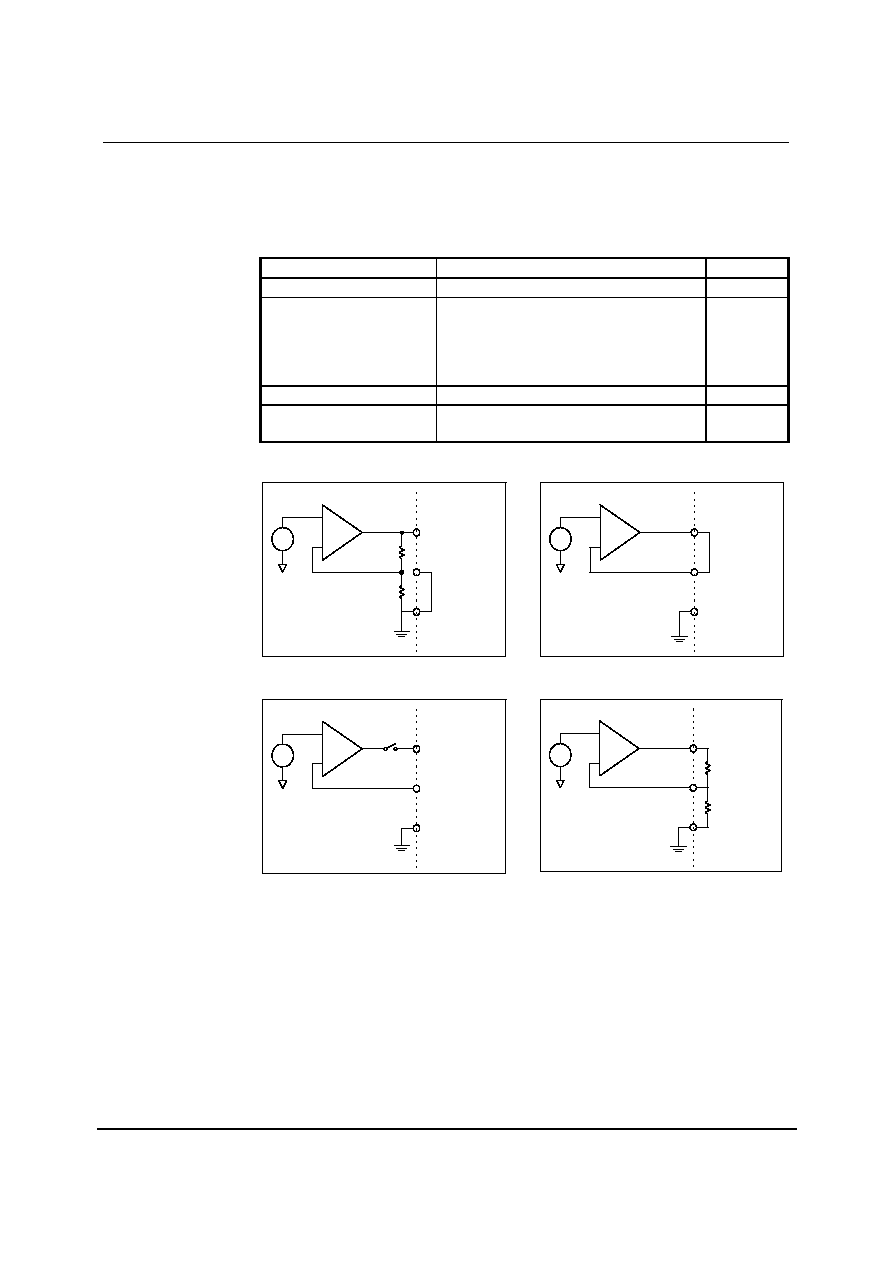
REFERENCE VOLTAGE GENERATION
The WM8200 incorporates an on-chip 0.5V bandgap voltage reference that can be used to derive a
temperature and supply independent voltage on pin VREF. The VREF output can be used for driving
external loads or setting the ADC input range. The voltage is programmed via connections made to
the REFSENSE pin as shown in Table 4.
REFSENSE VREF
output
Refer
to
AGND 1.0V
Figure
7
AVDD
Hi impedance � A1 amplifier disabled
If using the ADC reference generator then an
external VREF source must be applied to the
VREF pin.
Figure 8
Connect to VREF
0.5V
Figure 9
R network to VREF / AGND
Between 0.5 V and 1 V
VREF=0.5x(1+Ra/Rb)
Figure 10
Table 4: � VREF output control by REFSENSE connection
+
A1
-
+
0.5V
-
VREF
REFSENSE
AVSS
10k
10k
Figure 7: VREF=1V
+
A1
-
+
0.5V
-
VREF
REFSENSE = AVDD
AVSS
Figure 8: VREF=Hi Impedance
+
A1
-
+
0.5V
-
VREF
REFSENSE
AVSS
Figure 9: VREF=0.5V
+
A1
-
+
0.5V
-
VREF
REFSENSE
AVSS
Ra
Rb
Figure 10: VREF between 0.5 and 1V
When enabled, the on-chip voltage reference should be externally decoupled (see Reference
Decoupling Section for details).
In internal ADC references mode (MODE=AVDD), the voltages at REFT and REFB are:
REFT = (AVDD + VREF) / 2
REFB = (AVDD � VREF) / 2
If external ADC references mode (MODE=AVSS), the average value of the external voltages applied
to REFT and REFB should be AVDD/2 for correct device operation.
WM8200
Product Preview
w
PP Rev 1.22 March 2002
14
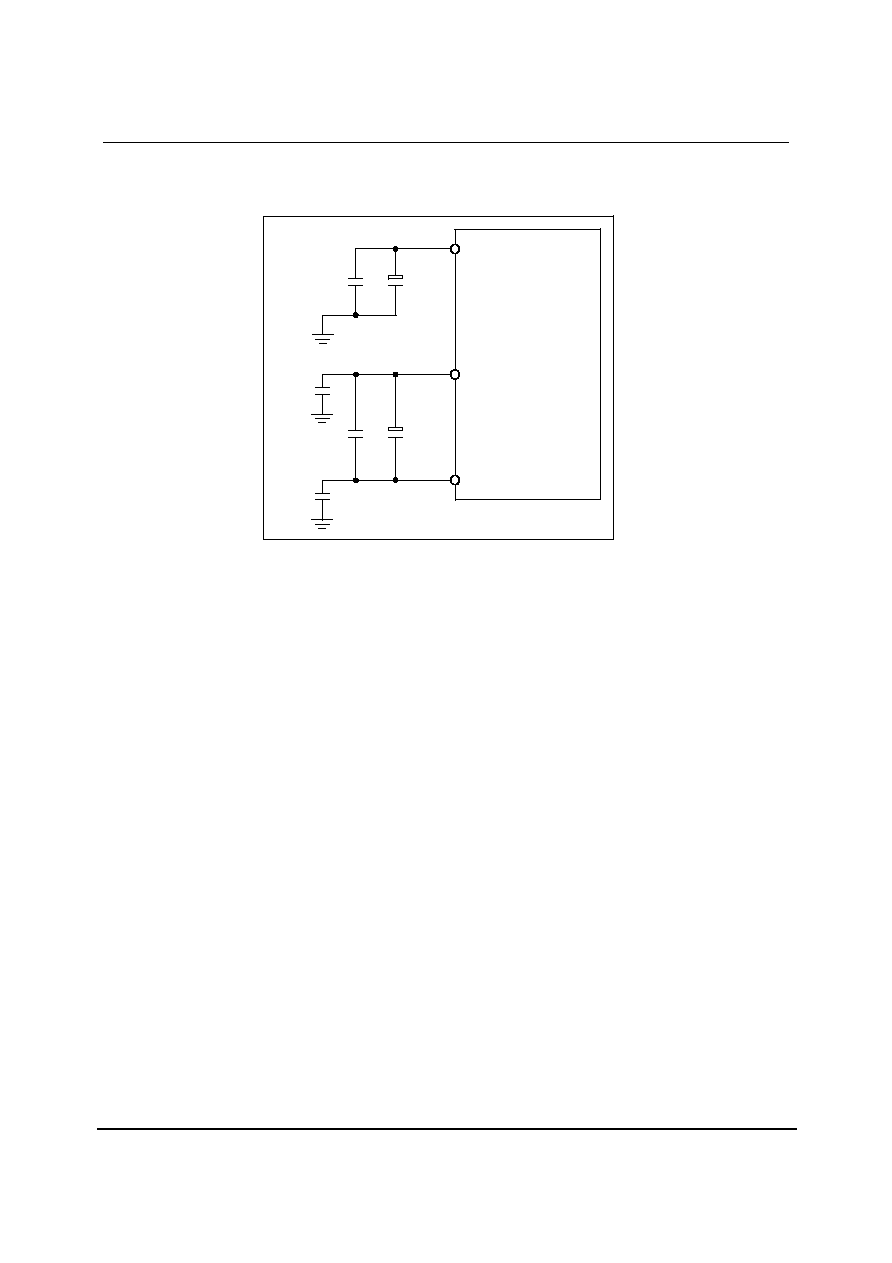
REFERENCE DECOUPLING
VREF, REFT and REFB must be decoupled as shown in Figure 11.
REFT
REFB
WM8200-10/12
100 nF
100 nF
100 nF
+
10
�
�
�
�
F
100 nF
+
VREF
10
�
�
�
�
F
Figure 11: VREF, REFT and REFB decoupling
WM8200
Product Preview
w
PP Rev 1.22 March 2002
15
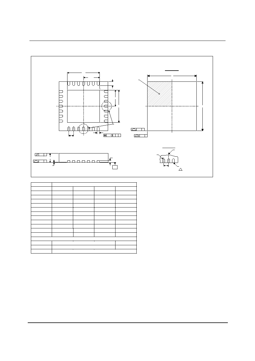
PACKAGE DIMENSIONS
DM023.C
FL: 28 PIN QFN PLASTIC PACKAGE 5
X
5
X
0.9 mm BODY, 0.50 mm LEAD PITCH
14
13
b
15
C
aaa
L
D2/2
D2
E2
E2/2
SEE DETAIL B
INDEX AREA
(D/2 X E/2)
C
aaa
2 X
2 X
C
C
0.08
C
ccc
A
A1
(A3)
SEATING PLANE
B
C
ccc
M
A
DETAIL B
TERMINAL TIP
R
1
NOTES:
1. DIMENSION b APPLIED TO METALLIZED TERMINAL AND IS MEASURED BETWEEN 0.25 mm AND 0.30 mm FROM TERMINAL TIP.
2. FALLS WITHIN JEDEC.95, MO-220 WITH THE EXCEPTION OF D2, E2, A3:
D2,E2: LARGER PAD SIZE CHOSEN WHICH IS JUST OUTSIDE JEDEC SPECIFICATION
A3: NOMINAL VALUE LESS THAN JEDEC
3. ALL DIMENSIONS ARE IN MILLIMETRES
4. THIS DRAWING IS SUBJECT TO CHANGE WITHOUT NOTICE.
Symbols
Dimensions (mm)
MIN
NOM
MAX
NOTE
A
0.80
0.90
1.00
b
0.18
0.23
0.30
1
D
5.00 BSC
D2
3.2
3.3
3.4
E
5.00 BSC
E2
3.2
3.3
3.4
e
0.5 BSC
L
0.35
0.4
0.45
2
2
A1
0
0.02
0.05
A3
0.2 REF
TOP VIEW
B
B
A
A
DATUM
e
R
b(min)/2
aaa
0.15
ccc
0.10
REF:
JEDEC.95, MO-220, VARIATION VHHD-1
Tolerances of Form and Position
2
27
28
1
2
7
8
21
22
e
D
E

WM8200
Product Preview
w
PP Rev 1.22 March 2002
16
IMPORTANT NOTICE
Wolfson Microelectronics Ltd (WM) reserve the right to make changes to their products or to discontinue any product or
service without notice, and advise customers to obtain the latest version of relevant information to verify, before placing
orders, that information being relied on is current. All products are sold subject to the WM terms and conditions of sale
supplied at the time of order acknowledgement, including those pertaining to warranty, patent infringement, and limitation
of liability.
WM warrants performance of its products to the specifications applicable at the time of sale in accordance with WM's
standard warranty. Testing and other quality control techniques are utilised to the extent WM deems necessary to support
this warranty. Specific testing of all parameters of each device is not necessarily performed, except those mandated by
government requirements.
In order to minimise risks associated with customer applications, adequate design and operating safeguards must be used
by the customer to minimise inherent or procedural hazards.
WM assumes no liability for applications assistance or customer product design. WM does not warrant or represent that
any license, either express or implied, is granted under any patent right, copyright, mask work right, or other intellectual
property right of WM covering or relating to any combination, machine, or process in which such products or services might
be or are used. WM's publication of information regarding any third party's products or services does not constitute WM's
approval, license, warranty or endorsement thereof.
Reproduction of information from the WM web site or datasheets is permissible only if reproduction is without alteration and
is accompanied by all associated warranties, conditions, limitations and notices. Representation or reproduction of this
information with alteration voids all warranties provided for an associated WM product or service, is an unfair and deceptive
business practice, and WM is not responsible nor liable for any such use.
Resale of WM's products or services with statements different from or beyond the parameters stated by WM for that
product or service voids all express and any implied warranties for the associated WM product or service, is an unfair and
deceptive business practice, and WM is not responsible nor liable for any such use.
ADDRESS:
Wolfson Microelectronics plc
Westfield House
26 Westfield Road
Edinburgh
EH11 2QW
Tel :: +44 (0)131 272 7000
Fax :: +44 (0)131 272 7001
Email :: sales@wolfsonmicro.com