Document Outline
- WM8510
- Mono CODEC with Speaker Driver
- DESCRIPTION
- FEATURES
- APPLICATIONS
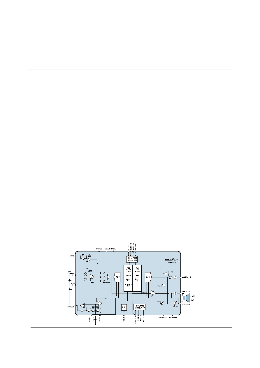
- BLOCK DIAGRAM
- TABLE OF CONTENTS
- PIN CONFIGURATION
- ORDERING INFORMATION
- PIN DESCRIPTION
- ABSOLUTE MAXIMUM RATINGS
- RECOMMENDED OPERATING CONDITIONS
- ELECTRICAL CHARACTERISTICS
- SIGNAL TIMING REQUIREMENTS
- SYSTEM CLOCK TIMING
- AUDIO INTERFACE TIMING Ö MASTER MODE
- AUDIO INTERFACE TIMING Ö SLAVE MODE
- CONTROL INTERFACE TIMING Ö 3--WIRE MODE
- CONTROL INTERFACE TIMING Ö 2--WIRE MODE
- DEVICE DESCRIPTION
- INTRODUCTION
- INPUT SIGNAL PATH
- ANALOGUE TO DIGITAL CONVERTER (ADC)
- INPUT LIMITER /AUTOMATIC LEVEL CONTROL (ALC)
- OUTPUT SIGNAL PATH
- ANALOGUE OUTPUTS
- OUTPUT SWITCH
- DIGITAL AUDIO INTERFACES
- AUDIO SAMPLE RATES
- MASTER CLOCK AND PHASE LOCKED LOOP (PLL)
- GENERAL PURPOSE INPUT/OUTPUT
- CONTROL INTERFACE
- RESETTING THE CHIP
- POWER SUPPLIES
- POWER MANAGEMENT
- REGISTER MAP
- DIGITAL FILTER CHARACTERISTICS
- TERMINOLOGY
- DAC FILTER RESPONSES
- DE-EMPHASIS FILTER RESPONSES
- HIGHPASS FILTER
- ADC FILTER RESPONSES
- PACKAGE DIAGRAM
- IMPORTANT NOTICE
- ADDRESS
w
WM8510
Mono CODEC with Speaker Driver
WOLFSON MICROELECTRONICS plc
w :: www.wolfsonmicro.com
Product Preview December 2004, Rev 1.2
Copyright
2004 Wolfson Microelectronics plc
DESCRIPTION
The WM8510 is a low power, high quality mono codec designed
for Voice over Internet Protocol (VoIP) and Digital Telephones.
The device integrates support for one pseudo-differential and
one single ended input (Handset Mic and Speaker Mic) and
includes drivers for speakers or headset, and mono line output,
making it ideal for Telephone designs. External component
requirements are reduced as no separate microphone or
earpiece amplifiers are required.
Advanced Sigma Delta Converters are used along with digital
decimation and interpolation filters to give high quality audio at
sample rates from 8 to 48ks/s.
Additional digital filtering options are available in the ADC path,
to cater for application filtering such as `wind noise reduction',
plus an advanced mixed signal ALC function with noise gate is
provided.
An on-chip PLL is provided to generate the required Master
Clock from an external reference clock. The PLL clock can also
be output if required elsewhere in the system.
The WM8510 operates at supply voltages from 2.5 to 3.6V,
although the digital core can operate at voltages down to 1.62V
to save power. The speaker and mono outputs use a separate
supply of up to 5V which enables increased output power if
required. Different sections of the chip can also be powered
down under software control by way of the selectable two or
three wire control interface.
WM8510 is supplied in a convenient 28-pin SSOP package,
offering high levels of functionality in easy to use package.
BLOCK DIAGRAM
FEATURES
∑ Mono Codec:
∑ Audio sample rates:8, 11.025, 16, 22.05, 24, 32, 44.1,
48kHz
∑ DAC SNR 93dB, THD -84dB (`A'-weighted @ 8 ≠ 48ks/s)
∑ ADC SNR 90dB, THD -80dB (`A'-weighted @ 8 ≠ 48ks/s)
∑ On-chip Headphone/Speaker Driver with `cap-less' connect
- 40mW output power into 16
/ 3.3V SPKVDD
- BTL speaker drive 0.8W into 8
/ 5V SPKVDD
∑ Earpiece Line output
∑ Multiple analog inputs, plus analog bypass path (0 or -10dB)
∑ Mic Preamps:
∑ Two Microphone Interfaces
- One pseudo-differential input
- One single ended input
- Programmable preamp gain
- Psuedo differential inputs with common mode rejection
- Programmable ALC / Noise Gate in ADC path
∑ Low-noise bias supplied for microphone
Other features
∑ Digital Playback Limiter
∑ Programmable ADC High Pass Filter (wind noise reduction)
∑ Programmable ADC Notch Filter
∑ On-chip PLL
∑ Low power, low voltage
- 2.5V to 3.6V (digital core: 1.62V to 3.6V)
- power consumption <10mA all-on 48ks/s mode
∑ 28 pin SSOP package
APPLICATIONS
∑ VoIP Telephones
∑ Digital Telephones
∑ Conference Speaker-phone
∑
Mobile Telephone Hands-free Kits
∑
General Purpose low power audio CODEC

WM8510
Product Preview
w
PP Rev 1.2 December 2004
2
TABLE OF CONTENTS
DESCRIPTION .......................................................................................................1
FEATURES.............................................................................................................1
APPLICATIONS .....................................................................................................1
PIN CONFIGURATION...........................................................................................3
ORDERING INFORMATION ..................................................................................3
PIN DESCRIPTION ................................................................................................4
ABSOLUTE MAXIMUM RATINGS .........................................................................5
RECOMMENDED OPERATING CONDITIONS .....................................................5
ELECTRICAL CHARACTERISTICS ......................................................................6
TERMINOLOGY ............................................................................................................ 8
SIGNAL TIMING REQUIREMENTS .......................................................................9
SYSTEM CLOCK TIMING ............................................................................................. 9
AUDIO INTERFACE TIMING ≠ MASTER MODE .......................................................... 9
AUDIO INTERFACE TIMING ≠ SLAVE MODE............................................................ 10
CONTROL INTERFACE TIMING ≠ 3-WIRE MODE .................................................... 11
CONTROL INTERFACE TIMING ≠ 2-WIRE MODE .................................................... 12
DEVICE DESCRIPTION .......................................................................................13
INTRODUCTION ......................................................................................................... 13
INPUT SIGNAL PATH ................................................................................................. 14
ANALOGUE TO DIGITAL CONVERTER (ADC).......................................................... 19
INPUT LIMITER / AUTOMATIC LEVEL CONTROL (ALC) .......................................... 22
OUTPUT SIGNAL PATH ............................................................................................. 26
ANALOGUE OUTPUTS............................................................................................... 30
OUTPUT SWITCH ...................................................................................................... 34
DIGITAL AUDIO INTERFACES................................................................................... 37
AUDIO SAMPLE RATES ............................................................................................. 43
MASTER CLOCK AND PHASE LOCKED LOOP (PLL) ............................................... 44
GENERAL PURPOSE INPUT/OUTPUT...................................................................... 46
CONTROL INTERFACE.............................................................................................. 46
RESETTING THE CHIP .............................................................................................. 47
POWER SUPPLIES .................................................................................................... 47
POWER MANAGEMENT ............................................................................................ 49
REGISTER MAP...................................................................................................50
DIGITAL FILTER CHARACTERISTICS ...............................................................51
TERMINOLOGY .......................................................................................................... 51
DAC FILTER RESPONSES......................................................................................... 52
ADC FILTER RESPONSES......................................................................................... 52
DE-EMPHASIS FILTER RESPONSES........................................................................ 53
HIGHPASS FILTER..................................................................................................... 54
PACKAGE DIAGRAM ..........................................................................................55
IMPORTANT NOTICE ..........................................................................................56
ADDRESS ................................................................................................................... 56
Product Preview
WM8510
w
PP Rev 1.2 December 2004
3
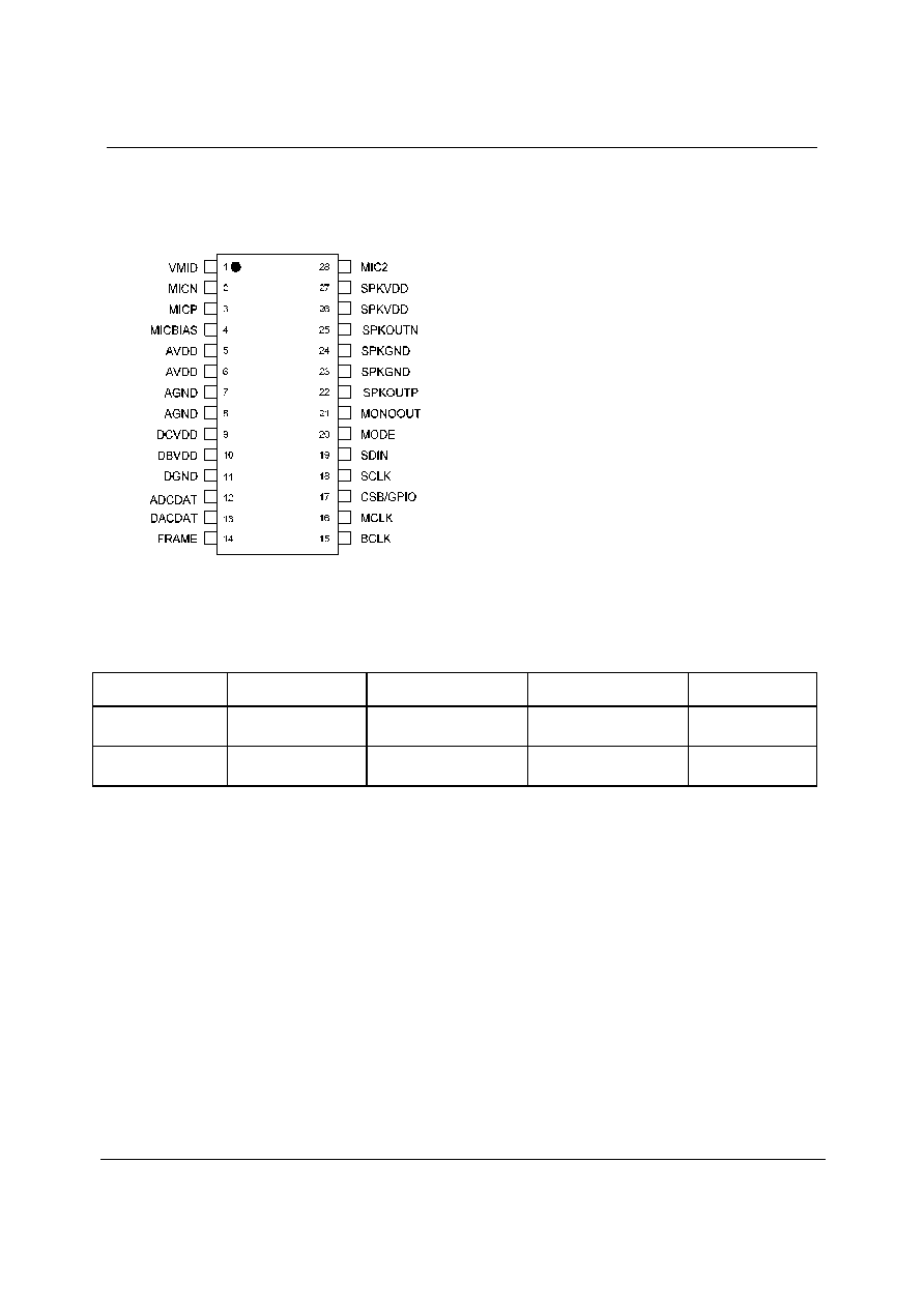
PIN CONFIGURATION
ORDERING INFORMATION
ORDER CODE
TEMPERATURE
RANGE
PACKAGE
MOISTURE SENSITIVITY
LEVEL
PACKAGE BODY
TEMPERATURE
WM8510GEDS/V
-25
∞C to +85∞C
28-pin SSOP
(lead free)
MSL3
260
o
C
WM8510GEDS/RV
-25
∞C to +85∞C
28-pin SSOP
(lead free, tape and reel)
MSL3
260
o
C
Note:
Reel Quantity = 2,000
WM8510
Product Preview
w
PP Rev 1.2 December 2004
4
PIN DESCRIPTION
PIN
NAME
TYPE
DESCRIPTION
1
VMID
Reference
Decoupling for midrail reference voltage
2
MICN
Analog Input
Microphone negative input
3
MICP
Analog Input
Microphone positive input (common mode)
4
MICBIAS
Analog Output
Microphone Bias
5
AVDD
Supply
Analogue supply (feeds ADC, DAC and PLL)
6
AVDD
Supply
Analogue supply (feeds ADC, DAC and PLL)
7
AGND
Supply
Analogue ground (feeds ADC, DAC and PLL)
8
AGND
Supply
Analogue ground (feeds ADC, DAC and PLL)
9
DCVDD
Supply
Digital Core supply
10
DBVDD
Supply
Digital Buffer (Input/Output) supply
11
DGND
Supply
Digital ground
12
ADCDAT
Digital Output
ADC Digital Audio Data Output
13
DACDAT
Digital Input
DAC Digital Audio Data Input
14
FRAME
Digital Input/Output
DAC and ADC Sample Rate Clock or Frame synch
15
BCLK
Digital Input/Output
Digital Audio Port Clock
16
MCLK
Digital Input
Master Clock Input
17
CSB/GPIO
Digital Input/Output
3-Wire MPU Chip Select or General Purpose Input/Output pin.
18
SCLK
Digital Input
3-Wire MPU Clock Input / 2-Wire MPU Clock Input
19
SDIN
Digital Input/Output
3-Wire MPU Data Input / 2-Wire MPU Data Input/Output
20
MODE
Digital Input
Control Interface Mode Selection Pin.
21
MONOOUT
Analog Output
Mono Audio Output
22
SPKOUTP
Analog Output
Speaker Output Positive
23
SPKGND
Supply
Speaker ground (feeds speaker and mono output amps only)
24
SPKGND
Supply
Speaker ground (feeds speaker and mono output amps only)
25
SPKOUTN
Analog Output
Speaker Output Negative
26
SPKVDD
Supply
Speaker supply (feeds speaker and mono output amps only)
27
SPKVDD
Supply
Speaker supply (feeds speaker and mono output amps only)
28
MIC2
Analog Input
Second Analog Input
Product Preview
WM8510
w
PP Rev 1.2 December 2004
5
ABSOLUTE MAXIMUM RATINGS
Absolute Maximum Ratings are stress ratings only. Permanent damage to the device may be caused by continuously
operating at or beyond these limits. Device functional operating limits and guaranteed performance specifications are given
under Electrical Characteristics at the test conditions specified.
ESD Sensitive Device. This device is manufactured on a CMOS process. It is therefore generically susceptible to
damage from excessive static voltages. Proper ESD precautions must be taken during handling and storage of this
device.
Wolfson tests its package types according to IPC/JEDEC J-STD-020B for Moisture Sensitivity to determine acceptable storage
conditions prior to surface mount assembly. These levels are:
MSL1 = unlimited floor life at <30
∞C / 85% Relative Humidity. Not normally stored in moisture barrier bag.
MSL2 = out of bag storage for 1 year at <30
∞C / 60% Relative Humidity. Supplied in moisture barrier bag.
MSL3 = out of bag storage for 168 hours at <30
∞C / 60% Relative Humidity. Supplied in moisture barrier bag.
The Moisture Sensitivity Level for each package type is specified in Ordering Information.
CONDITION
MIN
MAX
DBVDD, DCVDD, AVDD supply voltages
-0.3V
+3.63V
SPKVDD supply voltage
-0.3V
+7V
Voltage range digital inputs
DGND -0.3V
DVDD +0.3V
Voltage range analogue inputs
AGND -0.3V
AVDD +0.3V
Operating temperature range, T
A
-25
∞C
+85
∞C
Storage temperature after soldering
-65
∞C
+150
∞C
Notes
1.
Analogue and digital grounds must always be within 0.3V of each other.
2.
All digital and analogue supplies are completely independent from each other.
RECOMMENDED OPERATING CONDITIONS
PARAMETER
SYMBOL
TEST
CONDITIONS
MIN
TYP
MAX
UNIT
Digital supply range (Core)
DCVDD
1.62
3.6
V
Digital supply range (Buffer)
DBVDD
2.5
3.6
V
Analogue supplies range
AVDD
2.5
3.6
V
Speaker supply
SPKVDD
2.5
5.5
V
Ground
DGND,AGND, SPKGND
0
V