 | ÐлекÑÑоннÑй компоненÑ: WM8602 | СкаÑаÑÑ:  PDF PDF  ZIP ZIP |
Äîêóìåíòàöèÿ è îïèñàíèÿ www.docs.chipfind.ru
w
WM8602
2.1 Channel PWM Controller
WOLFSON MICROELECTRONICS plc
www.wolfsonmicro.com
Product Preview, May 2004, Rev 1.5
Copyright
2004 Wolfson Microelectronics plc
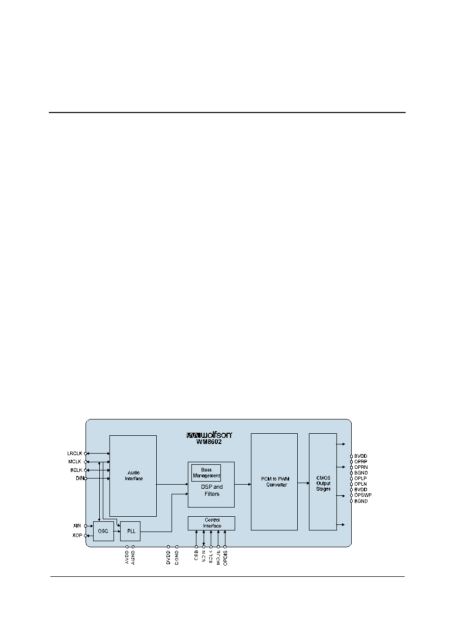
DESCRIPTION
The WM8602 comprises a high performance stereo + sub
PWM digital power amplifier controller. Simply by adding
appropriate power output stages a 2.1 channel power
amplifier may be built. Two identical full audio bandwidth
channels, plus a reduced bandwidth sub channel are
provided as PWM outputs.
The PCM to PWM converter supports up to 2 channels of
audio, in PCM input formats. The on board bass
management enables the generation of a sub channel from
the stereo PCM data.
A Graphic Equaliser function is provided, plus selectable
high frequency equalisation to suit different speaker types.
Independent volume control for each channel is provided.
The WM8602 PWM controller is compatible with integrated
switching output stages available from a number of vendors
or alternatively may be used with a discrete output stage
configuration and achieve similar levels of performance.
A Dynamic Peak Compressor with programmable attack
and decay times is included, which allows headroom for
tone control, bass management and extra digital gain to be
provided, without clipping occurring.
A Synchroniser allows slaving to LRCLK, thus making the
WM8602 independent of source MCLK frequency and jitter.
The device is controlled via a 2/3 wire serial interface. The
interface provides access to all features including channel
selection, volume controls, mutes, de-emphasis and power
management facilities. The device is supplied in a 28-pin
SSOP package.
FEATURES
·
Multi-channel PWM audio amplifier controller
·
Supports Stereo input
·
Supports stereo or 2.1 with sub channel generation
·
PWM Audio Performance with typical output stage
-
100dB SNR (`A' weighted @ 48kHz)
-
0.01% THD @ 1Watt
-
0.1% THD @ 30Watt
·
Integrated Bass Management support with adjustable filter
·
Integrated 4-band Graphic Equaliser
·
Adjustable output stage filter compensation for different
speakers
·
Volume control on each channel +24dB to -103.5dB in
0.5dB steps, with volume ramping and auto-mute
functions
·
Programmable Dynamic Peak Compressor avoids clipping
even at high volume settings
·
Internal PLL and optional crystal oscillator, supporting
Audio and MPEG standards
·
2/3-Wire MPU Serial Control Interface
·
Master or Slave Clocking Mode
·
Programmable Audio Data Interface Modes
-
I
2
S, Left, Right Justified or DSP
-
16/20/24/32 bit Word Lengths
·
De-emphasis support for stereo
·
CMOS digital outputs
APPLICATIONS
· Hi-Fi systems
· Automotive Audio
· Boombox
· Active Speakers

WM8602
Product Preview
w
PP Rev 1.5 May 2004
2
TABLE OF CONTENTS
DESCRIPTION .......................................................................................................1
FEATURES.............................................................................................................1
APPLICATIONS .....................................................................................................1
TABLE OF CONTENTS .........................................................................................2
PIN CONFIGURATION...........................................................................................3
ORDERING INFORMATION ..................................................................................3
ABSOLUTE MAXIMUM RATINGS .........................................................................5
ELECTRICAL CHARACTERISTICS ......................................................................6
TERMINOLOGY .....................................................................................................7
POWER CONSUMPTION ......................................................................................7
SIGNAL TIMING REQUIREMENTS .......................................................................8
POWER SUPPLY.......................................................................................................... 8
MASTER CLOCK TIMING ............................................................................................. 8
AUDIO INTERFACE TIMING MASTER MODE .......................................................... 9
DEVICE DESCRIPTION .......................................................................................14
INTRODUCTION ......................................................................................................... 14
SIGNAL PATH............................................................................................................. 14
DIGITAL AUDIO INTERFACE ..................................................................................... 15
AUDIO INTERFACE CONTROL.................................................................................. 18
MASTER CLOCK AND AUDIO SAMPLE RATES........................................................ 19
SYNCHRONISER........................................................................................................ 22
CONTROL INTERFACE OPERATION ........................................................................ 23
INPUT PROCESSOR .................................................................................................. 24
BASS MANAGEMENT .........................................................................................25
GRAPHIC EQUALISER............................................................................................... 26
DIGITAL DEEMPHASIS .............................................................................................. 28
DIGITAL VOLUME CONTROL .................................................................................... 28
SOFT MUTE AND AUTO-MUTE ................................................................................. 29
DYNAMIC PEAK COMPRESSOR ............................................................................... 31
INTERPOLATION FILTERS ........................................................................................ 34
PCM TO PWM CONVERTER ..................................................................................... 35
STANDBY, OUTPUT DISABLE AND RESET MODES ................................................ 36
EXTERNAL POWER SUPPLY CLOCK ....................................................................... 37
REGISTER MAP...................................................................................................39
FILTER RESPONSES ................................................................................................. 40
DIGITAL DE-EMPHASIS CHARACTERISTICS........................................................... 41
APPLICATION NOTES ........................................................................................42
START-UP .................................................................................................................. 42
POWER SUPPLY CONNECTIONS............................................................................. 43
APPLICATIONS INFORMATION .........................................................................44
RECOMMENDED EXTERNAL COMPONENTS .......................................................... 44
RECOMMENDED EXTERNAL COMPONENTS VALUES ........................................... 44
PACKAGE DIMENSIONS ....................................................................................45
IMPORTANT NOTICE ..........................................................................................46
ADDRESS: .................................................................................................................. 46
Product Preview
WM8602
w
PP Rev 1.5 May 2004
3
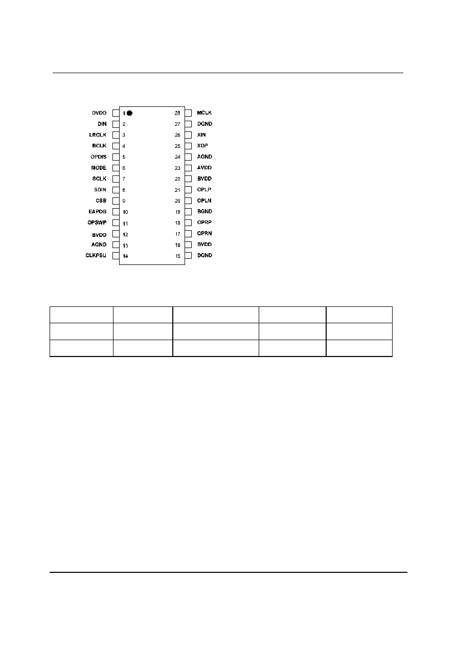
PIN CONFIGURATION
ORDERING INFORMATION
DEVICE
TEMPERATURE
RANGE
PACKAGE
MOISTURE LEVEL
SENSITIVITY
PEAK SOLDERING
TEMPERATURE
WM8602SEDS/V
-25 to + 85
°C
28-pin SSOP
(lead free)
MSL1
260°C
WM8602SEDS/RV
-25 to + 85
°C
28-pin SSOP
(lead free, tape and reel)
MSL1
260°C

WM8602
Product Preview
w
PP Rev 1.5 May 2004
4
PIN DESCRIPTION
PIN
NAME
TYPE
DESCRIPTION
1
DVDD
Supply
Digital positive supply
2
DIN
Digital Input
L/R channel data input
3
LRCLK
Digital Input/Output
Left/right word clock
4
BCLK
Digital IO
Audio interface bit clock
5
OPDIS
Digital Input p.d.
Output disable
6
MODE
Digital Input p.d.
2/3 Wire control interface mode
7
SCLK
Digital Input
Serial interface clock
8
SDIN
Digital Input/Output
Serial interface data
9
CSB
Digital Input
Serial interface load signal
10
EAPDB
Digital Output
External output stage power down
11
OPSWP
Digital Output
PWM output positive Subwoofer channel
12
BVDD
Supply
PWM output buffer positive supply
13
AGND
Supply
Analogue negative supply
14
CLKPSU
Digital Output
Clock for external PSU
15
BGND
Supply
PWM output buffer ground supply
16
BVDD
Supply
PWM output buffer positive supply
17
OPRN
Digital Output
PWM output negative right channel
18
OPRP
Digital Output
PWM output positive right channel
19
BGND
Supply
PWM output buffer ground supply
20
OPLN
Digital Output
PWM output negative left channel
21
OPLP
Digital Output
PWM output positive left channel
22
BVDD
Supply
PWM output buffer positive supply
23
AVDD
Analogue Supply
Analogue positive supply
24
AGND
Analogue Supply
Analogue negative supply
25
XOP
Digital Output
Crystal oscillator output connection
26
XIN
Digital Input
Crystal oscillator input connection (may be left unconnected in slave
mode)
27
DGND
Supply
Digital negative supply
28
MCLK
Digital Input/Output
Master clock; 256, 384, 512 fs (fs = word clock frequency) or 27MHz
Notes: Digital input pins have Schmitt trigger input buffers. Pins marked `p.u.' or `p.d.' have internal pull-up or pull down.
Product Preview
WM8602
w
PP Rev 1.5 May 2004
5
ABSOLUTE MAXIMUM RATINGS
Absolute Maximum Ratings are stress ratings only. Permanent damage to the device may be caused by continuously operating at
or beyond these limits. Device functional operating limits and guaranteed performance specifications are given under Electrical
Characteristics at the test conditions specified.
ESD Sensitive Device. This device is manufactured on a CMOS process. It is therefore generically susceptible
to damage from excessive static voltages. Proper ESD precautions must be taken during handling and storage
of this device.
Wolfson tests its package types according to IPC/JEDEC J-STD-020B for Moisture Sensitivity to determine acceptable storage
conditions prior to surface mount assembly. These levels are:
MSL1 = unlimited floor life at <30
°C / 85% Relative Humidity. Not normally stored in moisture barrier bag.
MSL2 = out of bag storage for 1 year at <30
°C / 60% Relative Humidity. Supplied in moisture barrier bag.
MSL3 = out of bag storage for 168 hours at <30
°C / 60% Relative Humidity. Supplied in moisture barrier bag.
The Moisture Sensitivity Level for each package type is specified in Ordering Information.
CONDITION
MIN
MAX
Analogue supply voltage (AVDD)
-0.3V
+5V
Digital supply voltage (DVDD)
-0.3V
+5V
PWM output buffer supply voltage (BVDD)
-0.3V
+5V
Voltage range inputs
DGND -0.3V
DVDD +0.3V
Master Clock Frequency
10MHz
50MHz
Operating temperature range, T
A
-20
°C
+85
°C
Storage temperature
-65
°C
+150
°C
Notes:
1.
GND power supplies (i.e. AGND, DGND, and BGND) must always be within 0.3V of each other.
2.
VDD power supplies (i.e. AVDD, DVDD, and BVDD) must always be within 0.3V of each other.
RECOMMENDED OPERATING CONDITIONS
PARAMETER
SYMBOL
TEST CONDITIONS
MIN
TYP
MAX
UNIT
Analogue supply range
AVDD
2.7
3.6
V
Digital supply range
DVDD
2.7
3.6
V
PWM output buffer supply
BVDD
2.7
3.6
V
Ground
AGND, DGND, BGND
0
V

WM8602
Product Preview
w
PP Rev 1.5 May 2004
6
ELECTRICAL CHARACTERISTICS
Test Conditions
AVDD, BVDD, DVDD = 2.7 to 3.3V, AGND, DGND, BGND = 0V, T
A
= -20 to +85
o
C, fs = 44.1kHz/48kHz, MCLK = 256fs unless
stated.
PARAMETER
SYMBOL
TEST CONDITIONS
MIN
TYP
MAX
UNIT
Input capacitance
C
i
3
4
pF
Input leakage
I
leak
±0.1
±0.5
µA
Oscillator
Input XIN LOW level
VX
IL
0
0.44
V
Input XIN HIGH level
VX
IH
0.77
AVDD
V
Input XIN capacitance
C
XI
4
5
pF
Input XIN leakage
IX
leak
0.10
0.11
0.13
mA
Output XOP LOW
VX
OL
15pF load capacitors
0.1
0.4
0.5
V
Output XOP HIGH
VX
OH
15pF load capacitors
1.2
1.3
1.4
V
Digital Logic Levels (CMOS Levels)
Input LOW level
V
IL
0.3 x DVDD
V
Input HIGH level
V
IH
0.7 x DVDD
V
Pull-up/pull-down resistance
100
200
400
k
Output LOW
V
OL
I
OL
=+1mA
0.1 x DVDD
V
Output HIGH
V
OH
I
OL
=-1mA
0.9 x DVDD
V
Digital Logic Levels (LVDS Levels)
Output differential voltage
V
OD
R
T
=100
200
350
500
mV
Offset voltage
V
OS
R
T
=100
0.95
1.25
1.4
V
Termination load
R
T
20pF load
100
PCM to PWM converter
Digital SNR
L, R
105
dB
Typical SNR with output stage
(A-weighted)
L, R
100
dB
Typical Dynamic Range with
output stage
L, R
100
dB
Digital THD+N at 0dBfs
L, R
0.001
%
Typical THD+N at 30Watt with
output stage
L, R
0.1
%
Typical THD+N at 1Watt with
typical output stage
L, R
0.01
%
Typical IMD (CCIF 19/20kHz)
L, R
-70
dBFS
Typical IMD (SMPTE
60Hz/7kHz)
L, R
-70
dBFS
PCM to PWM converter
Digital SNR
Subwoofer
5
105
Typical SNR with output stage
(A-weighted)
Subwoofer
5
100
Typical Dynamic Range with
output stage
Subwoofer
5
100
Digital THD+N at 0dBfs
Subwoofer
5
0.001
Typical THD+N at 30Watt with
output stage
Subwoofer
5
0.1
Typical THD+N at 1Watt with
typical output stage
Subwoofer
5
0.01
Typical IMD (CCIF 19/20kHz)
Subwoofer
5
-70
Typical IMD (SMPTE
60Hz/7kHz)
Subwoofer
5
-70
Product Preview
WM8602
w
PP Rev 1.5 May 2004
7
Test Conditions
AVDD, BVDD, DVDD = 2.7 to 3.3V, AGND, DGND, BGND = 0V, T
A
= -20 to +85
o
C, fs = 44.1kHz/48kHz, MCLK = 256fs unless
stated.
PARAMETER
SYMBOL
TEST CONDITIONS
MIN
TYP
MAX
UNIT
PWM buffer drive strength
I
source
CMOS
25
4
mA
I
sink
20pF load
25
4
mA
fs = 44.1kHz
352.8
kHz
PWM pulse repetition rate
f
PWM
fs = 48kHz
384
kHz
Notes:
1.
Ratio of output level with 1kHz full scale input, to the output level with all zeros into the digital input, measured `A'
weighted over a 20Hz to 20kHz bandwidth.
2.
All performance measurements done with 20kHz AES17 low pass filter, except where noted an A-weight filter is used.
Failure to use such a filter will result in higher THD+N and lower SNR and Dynamic Range readings than are found in
the Electrical Characteristics. The low pass filter removes out of band noise; although it is not audible it may affect
dynamic specification values.
3.
The XIN input supports both a clock as well as a crystal input.
4.
Parameter guaranteed by design.
5.
Validated using the following filter
PARAMETER
SYMBOL
TEST CONDITIONS
MIN
TYP
MAX
UNIT
Filter
Stopband
-3dB
1.00
kHz
Note: A third order differential RC filter has been used
TERMINOLOGY
1.
Signal-to-noise ratio (dB) - SNR is a measure of the difference in level between the full scale output and the output
with no signal applied.
2.
Dynamic range (dB) - DNR is a measure of the difference between the highest and lowest portions of a signal.
Normally a THD+N measurement at 60dB below full scale. The measured signal is then corrected by adding the 60dB
to it (e.g. THD+N @ -60dB= -32dB, DR= 92dB).
3.
THD+N (dB) - THD+N is a ratio, of the RMS values, of (Noise + Distortion)/Signal.
POWER CONSUMPTION
MODE DESCRIPTION
TYPICAL SUPPLY CURRENTS
[mA]
TOTAL CURRENT
[mA]
TOTAL POWER
[mW]
I
AVDD
I
DVDD
I
BVDD
AVDD, DVDD, BVDD = 3.3V
OFF
0
0
0
0
0
Standby
0.02
0.28
0
0.30
0.99
Mute
1.76
27.2
7.55
36.5
121
Stereo
1.76
27.7
7.55
37.0
122
2.1
Table 1 Supply Current Consumption
Notes:
1.
T
A
= +25
o
C, Slave Mode, fs = 48kHz, MCLK = 27 kHz, 24-bit data
2.
All figures are kHz 1kHz input sine wave @ 0dB.
WM8602
Product Preview
w
PP Rev 1.5 May 2004
8
SIGNAL TIMING REQUIREMENTS
POWER SUPPLY
Test Conditions
AGND, DGND, BGDN = 0V, T
A
= +25
°
C
PARAMETER
SYMBOL
MIN
TYP
MAX
UNIT
Power Supply Timing Information
AVDD: rise time 10% to 90% AVDD
t
AR
0.2
50
ms
DVDD: rise time 10% to 90% DVDD
t
DR
0.2
50
ms
BVDD: rise time 10% to 90% BVDD
t
BR
0.2
50
ms
Table 2 Power Supply Timing Requirements
MASTER CLOCK TIMING
XTI/MCLK
t
MCLKY
Figure 1 Master Clock Timing Requirements
Test Conditions
AVDD, DVDD, BVDD = 3.3V, AGND, DGND, BGDN = 0V, T
A
= +25
°
C
PARAMETER
SYMBOL
MIN
TYP
MAX
UNIT
System Clock Timing Information
XTI/MCLK System clock cycle time
t
MCLKY
20
100
ns
XTI/MCLK Duty cycle
40:60
60:40
%
XTI/MCLK Period Jitter
200
ps
XTI/MCLK Rise/Fall times 10% to 90% AVDD
3
ns
Table 3 Master Clock Timing Requirements
Product Preview
WM8602
w
PP Rev 1.5 May 2004
9
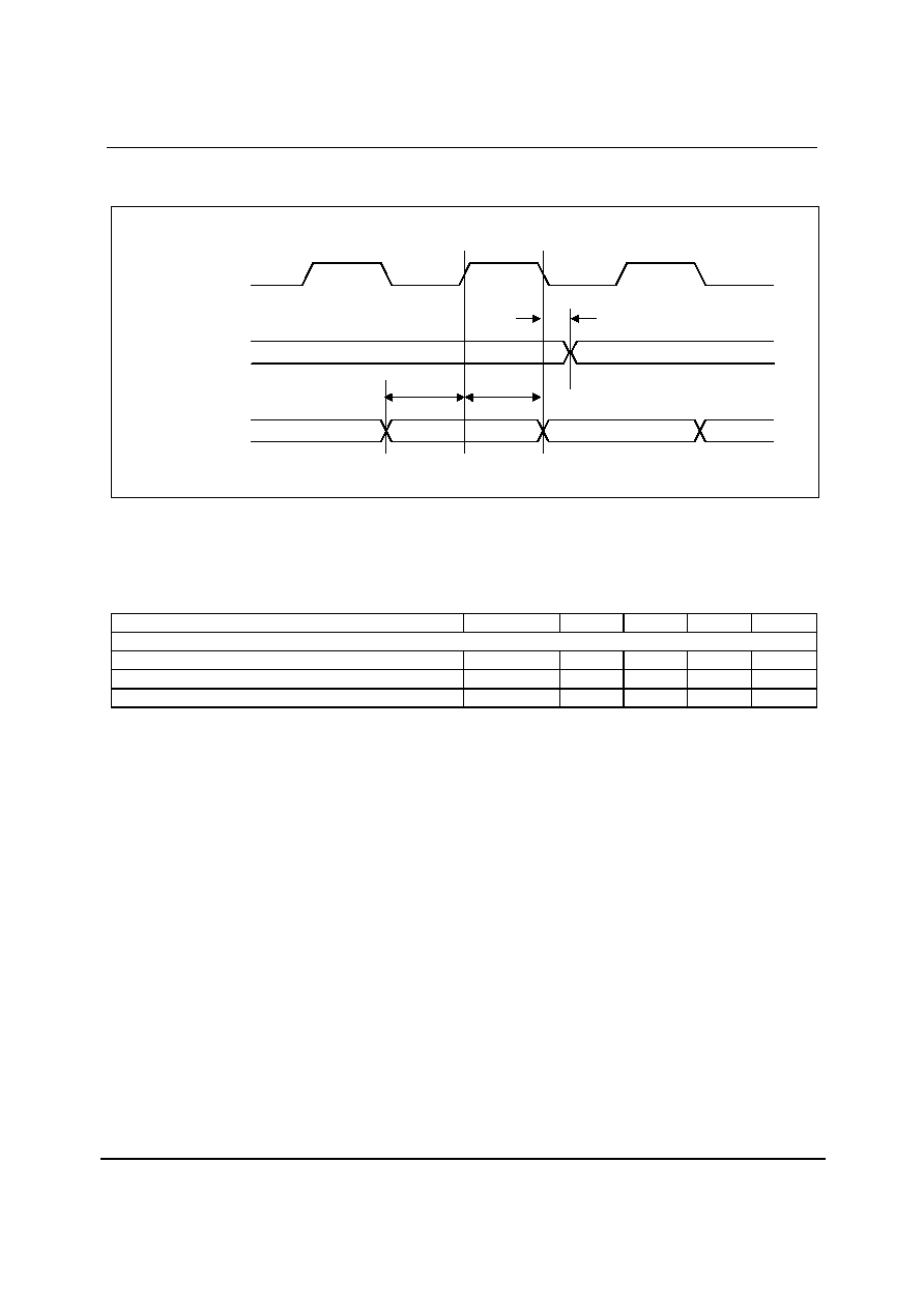
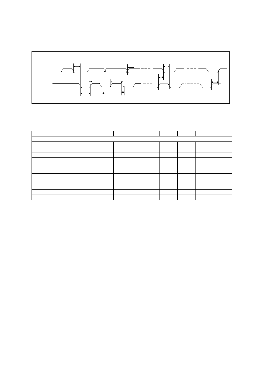
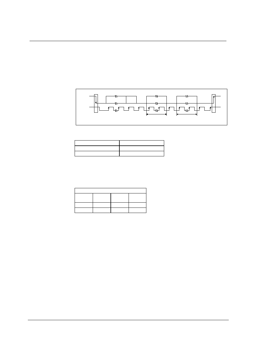
AUDIO INTERFACE TIMING MASTER MODE
Figure 2 Digital Audio Data Timing Master Mode (see Control Interface)
Test Conditions
AVDD, DVDD, BVDD = 3.3V, AGND, DGND, BGDN = 0V, T
A
= +25
o
C, Slave Mode, fs = 48kHz, MCLK = 256fs, 24-bit data,
unless otherwise stated.
PARAMETER
SYMBOL
MIN
TYP
MAX
UNIT
Audio Data Input Timing Information
LRCLK propagation delay from BCLK falling edge
t
DL
10
ns
DIN setup time to BCLK rising edge
t
DST
10
ns
DIN hold time from BCLK rising edge
t
DHT
10
ns
Table 4 Audio Interface Timing Master Mode
BCLK
(Output)
LRCLK
(Output)
t
DL
DIN
t
DHT
t
DST
WM8602
Product Preview
w
PP Rev 1.5 May 2004
10
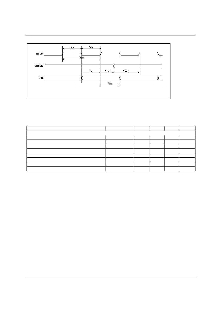
AUDIO INTERFACE TIMING SLAVE MODE
Figure 3 Digital Audio Data Timing Slave Mode
Test Conditions
AVDD, DVDD, BVDD = 3.3V, AGND, DGND, BGND = 0V, T
A
= +25
o
C, Slave Mode, fs = 48kHz, MCLK = 256fs, 24-bit data,
unless otherwise stated.
PARAMETER
SYMBOL
MIN
TYP
MAX
UNIT
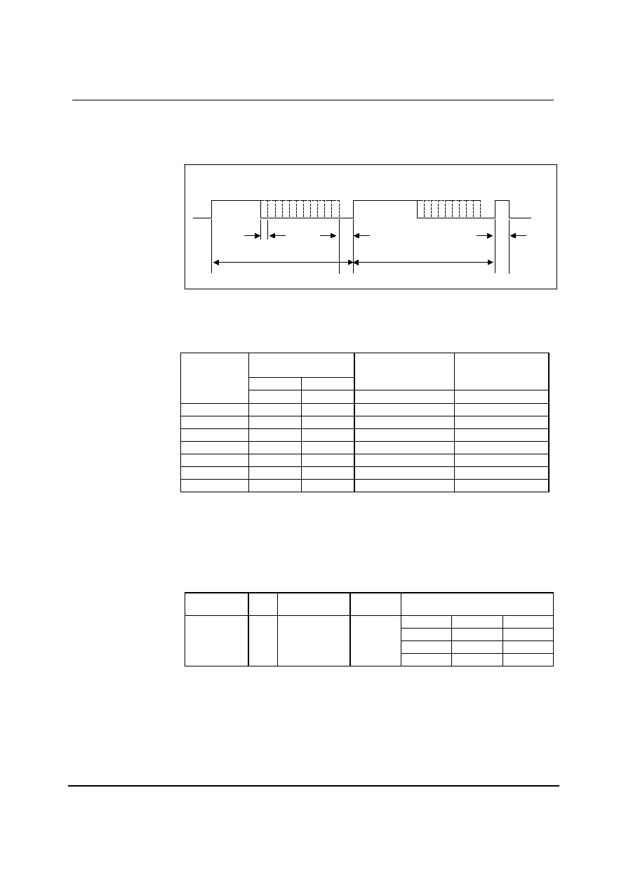
Audio Data Input Timing Information
BCLK cycle time
t
BCY
50
ns
BCLK pulse width high
t
BCH
20
ns
BCLK pulse width low
t
BCL
20
ns
BCLK rise/fall times
5
ns
LRCLK set-up time to BCLK rising edge
t
LRSU
10
ns
LRCLK hold time from BCLK rising edge
t
LRH
10
ns
LRCLK rise/fall times
5
ns
DIN hold time from BCLK rising edge
t
DH
10
ns
Table 5 Audio Interface Timing Slave Mode
Note: BCLK period should always be greater than or equal to MCLK period.
Product Preview
WM8602
w
PP Rev 1.5 May 2004
11
CONTROL INTERFACE TIMING 3-WIRE MODE
CSB
SCLK
SDIN
t
CSL
t
DHO
t
DSU
t
CSH
t
SCY
t
SCH
t
SCL
t
SCS
LSB
t
CSS
Figure 4 Control Interface Timing 3-Wire Serial Control Mode
Test Conditions
AVDD, DVDD, BVDD = 3.3V, AGND, DGND, BGND = 0V, T
A
= +25
o
C, Slave Mode, fs = 48kHz, MCLK = 256fs, 24-bit data,
unless otherwise stated.
PARAMETER
SYMBOL
MIN
TYP
MAX
UNIT
Program Register Input Information
SCLK rising edge to CSB rising edge
t
SCS
60
ns
SCLK pulse cycle time
t
SCY
80
ns
SCLK pulse width low
t
SCL
30
ns
SCLK pulse width high
t
SCH
30
ns
SDIN to SCLK set-up time
t
DSU
20
ns
SCLK to SDIN hold time
t
DHO
20
ns
CSB pulse width low
t
CSL
20
ns
CSB pulse width high
t
CSH
20
ns
CSB rising to SCLK rising
t
CSS
20
ns
Pulse width of spikes that will be suppressed
t
ps
2
8
ns
Table 6 Control Interface Timing 3-Wire Serial Control Mode
WM8602
Product Preview
w
PP Rev 1.5 May 2004
12
CONTROL INTERFACE TIMING 2-WIRE MODE
SDIN
SCLK
t
3
t
1
t
6
t
2
t
7
t
5
t
4
t
3
t
8
t
10
Figure 5 Control Interface Timing 2-Wire Serial Control Mode
Test Conditions
AVDD, DVDD, BVDD = 3.3V, AGND, DGND, BGND = 0V, T
A
= +25
o
C, Slave Mode, fs = 48kHz, MCLK = 256fs, 24-bit data,
unless otherwise stated.
PARAMETER
SYMBOL
MIN
TYP
MAX
UNIT
Program Register Input Information
SCLK Frequency
400
kHz
SCLK Low Pulse-Width
t
1
600
ns
SCLK High Pulse-Width
t
2
1.3
us
Hold Time (Start Condition)
t
3
600
ns
Setup Time (Start Condition)
t
4
600
ns
Data Setup Time
t
5
100
ns
SDIN, SCLK Rise Time
t
6
300
ns
SDIN, SCLK Fall Time
t
7
300
ns
Setup Time (Stop Condition)
t
8
600
ns
Data Hold Time
t
9
900
ns
Pulse width of spikes that will be suppressed
t
ps
2
8
ns
Table 7 Control Interface Timing 2-Wire Serial Control Mode
Product Preview
WM8602
w
PP Rev 1.5 May 2004
13
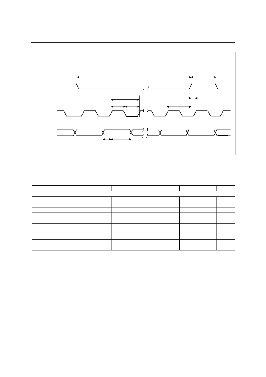
PWM OUTPUT TIMING
OPXXX
t
PWMH
t
PWML
t
PWMCY
Figure 6 PWM Output Timing
Test Conditions
AVDD, DVDD, BVDD = 2.7 to 3.3V, AGND, DGND, BGND = 0V, T
A
= -20 to +85
o
C, Slave Mode, fs = 48kHz, MCLK = 256fs,
24-bit data, unless otherwise stated.
PARAMETER
SYMBOL/NOTE
MIN
TYP
MAX
UNIT
Program Register Input Information
PWM Frequency
t
PWMCY
384
kHz
PWM Low Pulse-Width
t
PWML
122
ns
PWM High Pulse-Width
t
PWMH
122
ns
CMOS Mode
PWM Rise Time
1
20pF load
1.5
2.3
ns
PWM Fall Time
1
20pF load
1.5
2.3
ns
Table 8 PWM Interface Timing
Note:
1.
Parameter guaranteed by design
WM8602
Product Preview
w
PP Rev 1.5 May 2004
14
DEVICE DESCRIPTION
INTRODUCTION
The WM8602 is a high-performance multi-channel Pulse-Width Modulation (PWM) digital power
amplifier controller. The device accepts up to 2 channels of audio in PCM input format, and outputs 2
PWM full-bandwidth channels, plus a PWM sub-woofer channel. The outputs are suitable for directly
driving integrated switching output stages available from a number of vendors. The device is also
compatible with discrete MOSFET output stages. In both cases, Wolfson Microelectronics offer
Reference Designs for complete PWM digital power amplifiers.
The WM8602 has a configurable input processor which accepts Stereo channels of PCM audio and
outputs Stereo or 2.1 outputs. The sub channel is generated from the filtered sum of the low
frequency components of the input data.
The device has a Bass Management function, which has low-pass and high-pass filters for feeding
the sub channel and main output channels. It also provides selectable boost for the LFE channel.
Each channel can be configured to drive either "large" full-range speakers or "small" satellite
speakers with limited bass capability.
A Tone Control function is provided, plus selectable high frequency equalisation to compensate for
different loudspeaker characteristics. Independent volume control is provided for all channels, with
comprehensive mute features.
A Dynamic Peak Compressor with programmable attack and decay times is included, which allows
headroom for tone control, bass management and extra digital gain to be provided, without clipping
occurring.
The device is controlled via a 2/3 wire serial interface. The interface provides access to all features
including channel selection, volume controls, mute, de-emphasis and power management facilities.
SIGNAL PATH
The WM8602 receives digital input data via a 2-channel digital audio interface. The data is processed
in turn by the Input Processor, Bass Management and Equalisation, Volume Control and Dynamic
Peak Compressors, Interpolation Filters, and PCM-PWM Converters, as shown in Figure 7. The
PWM signals are output via CMOS drivers.
Figure 7 Signal Processing Block Diagram
Volume Control / Dynamic
Peak Compressors
PCM - PWM Converter
Interpolation Filters
Input Processor
Bass Management and
Equalisation
CMOS Output
2 Channel Input
Product Preview
WM8602
w
PP Rev 1.5 May 2004
15
Parameter
Group Delay
Unit
fs=48kHz
Unit
L / R channel
47
samples
1.0
ms
SUB channel
22
samples
0.5
ms
Table 9 Signal Path Group Delay
Note: The shorter delay on the SUB channel will not significantly affect audio performance. (It is
equivalent to moving the subwoofer forwards by about 15cm.)
DIGITAL AUDIO INTERFACE
The digital audio interface is used for inputting audio data into the WM8602. It uses five pins:
·
DIN: L+R channel data input
·
LRCLK: Data alignment clock
·
BCLK: Bit clock, for synchronisation
The clock signals BCLK and LRCLK can be outputs when the WM8602 operates as a master, or
inputs when it is a slave (see Master and Salve Mode Operation, below).
MASTER AND SLAVE MODE OPERATION
The WM8602 can be configured as either a master or slave mode device. As a master device the
WM8602 generates BCLK and LRCLK and thus controls sequencing of the data transfer on the data
channels. In slave mode, the WM8602 receives data and clock signals over the digital audio
interface. The mode can be selected by writing to the MS bit (see Table 23). Master and slave modes
are illustrated below.
Master Mode
Slave Mode
Figure 8 Operation Mode
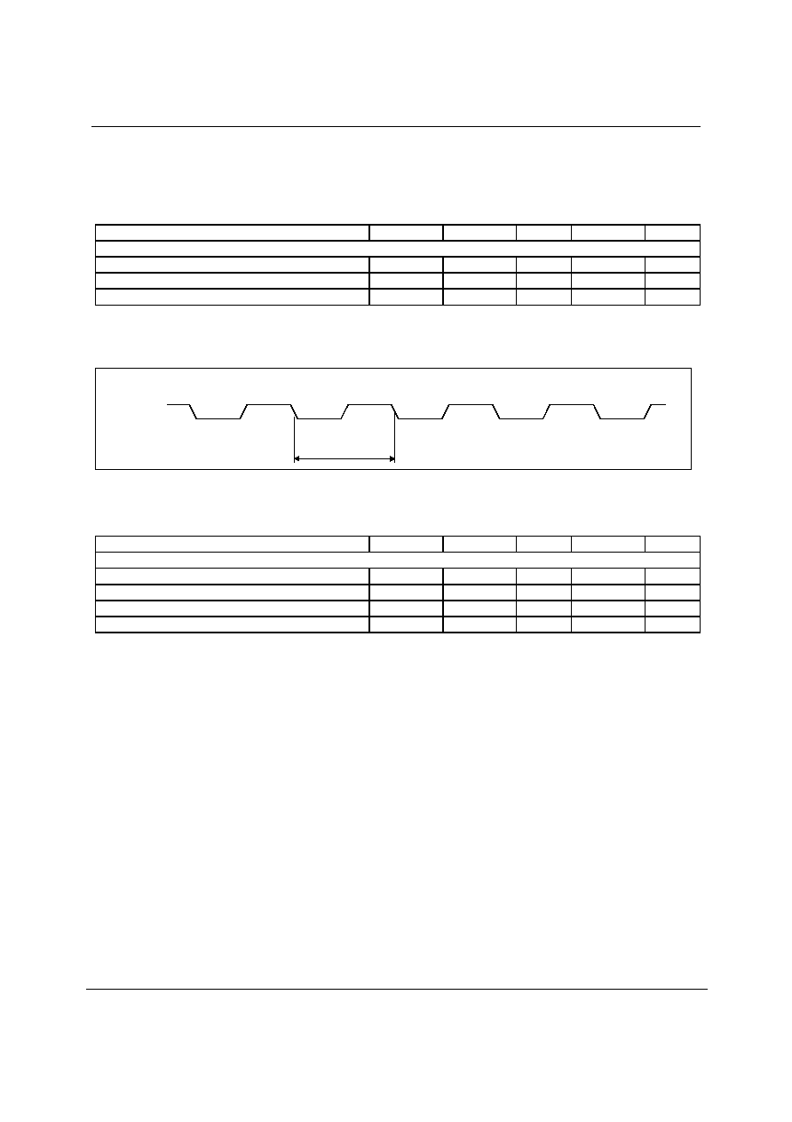
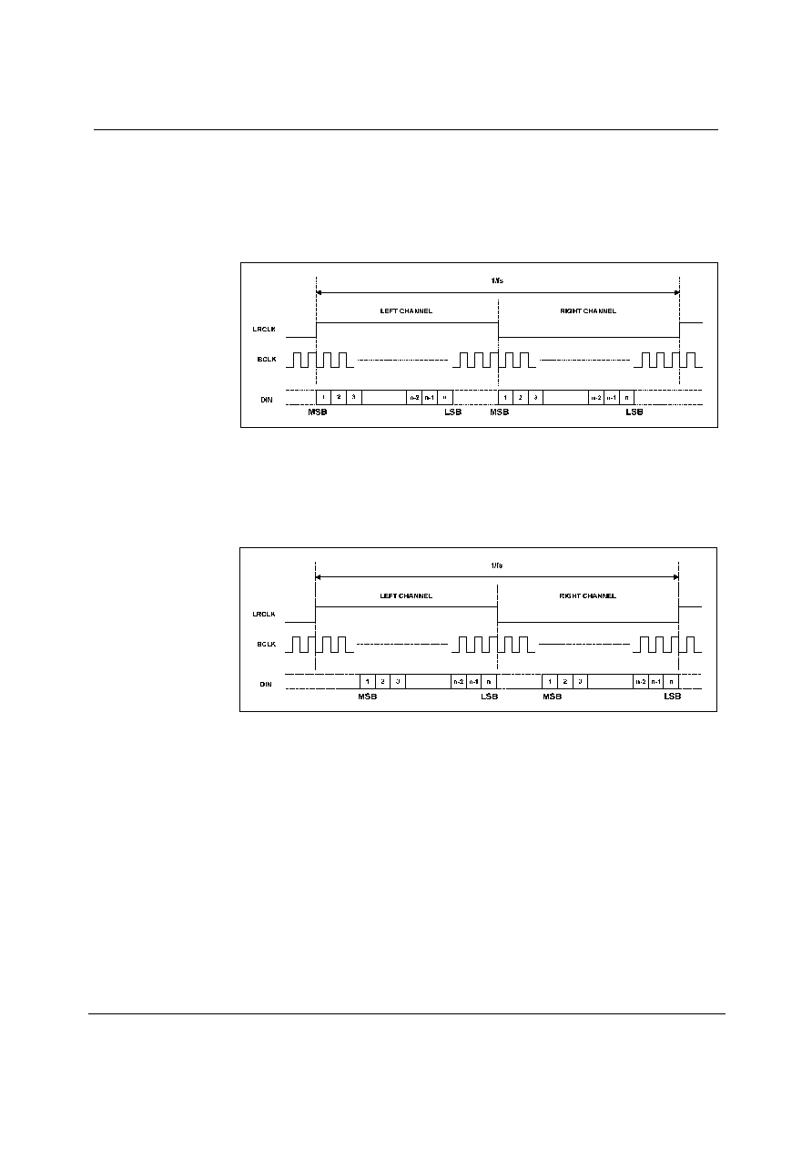
AUDIO DATA FORMATS
In Left Justified mode, the MSB is available on the first rising edge of BCLK following a LRCLK Audio
data is applied to the internal filters via the Digital Audio Interface. 5 popular interface formats are
supported:
·
Left Justified mode
·
Right Justified mode
·
I
2
S mode
·
DSP mode A
·
DSP mode B
All 5 formats send the MSB first and support word lengths of 16, 20, 24 and 32 bits. Except that 32
bit data is not supported in right justified mode. DIN and LRCLK are sampled on the rising, or falling
edge of BCLK.
In left justified, right justified and I
2
S modes the digital audio interface receives data on the DIN input.
Audio Data for each stereo channel is time multiplexed with LRCLK indicating whether the left or right
channel is present. LRCLK is also used as a timing reference to indicate the beginning or end of the
data words.
In left justified, right justified and I
2
S modes, the minimum number of BCLKs per DACLRC period is 2
times the selected word length. LRCLK must be high for a minimum of word length BCLKs and low
for a minimum of word length BCLKs. Any mark to space ratio on LRCLK is acceptable provided the
above requirements are met.
WM8602
Product Preview
w
PP Rev 1.5 May 2004
16
In DSP mode A or B, all channels are time multiplexed onto DIN. LRCLK is used as a frame sync
signal to identify the MSB of the first word. The minimum number of BCLKs per LRCLK period is 8
times the selected word length. Any mark to space ratio is acceptable on LRCLK provided the rising
edge is correctly positioned (see Figure 9, Figure 10 and Figure 11).
LEFT JUSTIFIED MODE
In left justified mode, the MSB is sampled on the first rising edge of BCLK following a LRCLK
transition. LRCLK is high during the left samples and low during the right samples.
Figure 9 Left Justified Mode Timing Diagram
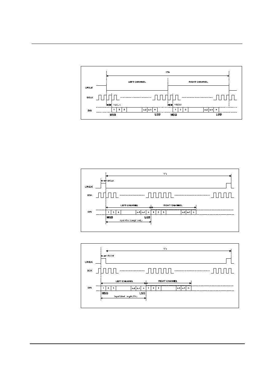
RIGHT JUSTIFIED MODE
In right justified mode, the LSB is sampled on the rising edge of BCLK preceding a LRCLK transition.
LRCLK is high during the left samples and low during the right samples.
Figure 10 Right Justified Mode Timing Diagram
Product Preview
WM8602
w
PP Rev 1.5 May 2004
17
I
2
S MODE
In I
2
S mode, the MSB is sampled on the second rising edge of BCLK following a LRCLK transition.
LRCLK is low during the left samples and high during the right samples.
Figure 11 I
2
S Mode Timing Diagram
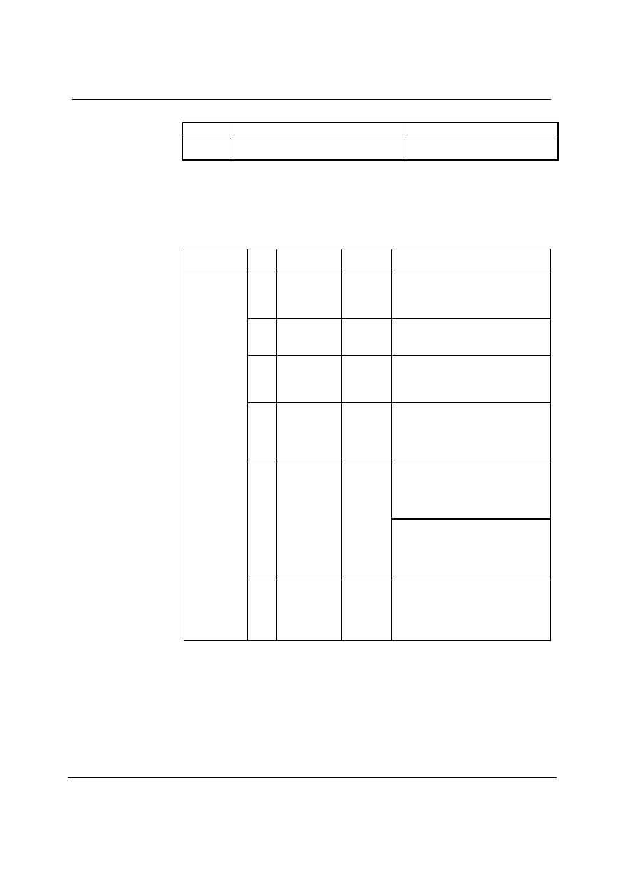
DSP MODE A AND B
In DSP mode, the Left channel MSB is available on either the 1
st
(mode B) or 2
nd
(mode A) rising
edge of BCLK (selectable by LRP) following a rising edge of LRCLK. Right channel data immediately
follows left channel data. Depending on word length, BCLK frequency and sample rate, there may be
unused BCLK cycles between the LSB of the right channel data and the next sample.
Figure 12 DSP Mode A Timing Diagram
Figure 13 DSP Mode B Timing Diagram
WM8602
Product Preview
w
PP Rev 1.5 May 2004
18
No BCLK edges are allowed between the data words.
MODE
INPUT FORMAT (ORDER)
SUPPORTED MODES
Stereo
L, R
No restrictions apply
Table 10 DSP Mode Input Format
AUDIO INTERFACE CONTROL
The register bits controlling audio format, word length and master/slave mode are summarised
below. MS selects audio interface operation in master or slave mode. In Master mode BCLK and
LRCLK are outputs and the frequency of LRCLK is set by the sample rate control bits SR[3:0]. In
Slave mode BCLK and LRCLK are inputs (refer to Table 12 for sample rate control in this case).
REGISTER
ADDRESS
BIT
LABEL
DEFAULT
DESCRIPTION
8
BCLKINV
0
BCLK invert bit (for master and slave
modes)
0 = BCLK not inverted
1 = BCLK inverted
7
MS
0
Master / Slave Mode Control
1 = Enable Master Mode
0 = Enable Slave Mode
6
LRSWAP
0
Left/Right channel swap
1 = swap left and right data in audio
interface
0 = output left and right data as normal
4
LRP
0
Right, left and I
2
S modes LRCLK
polarity
1 = invert LRCLK polarity
0 = normal LRCLK polarity
(as show in e.g. Figure 12)
DSP Mode A/B select
1 = MSB is available on 1st BCLK rising
edge after LRC rising edge (mode B)
0 = MSB is available on 2nd BCLK rising
edge after LRC rising edge (mode A)
3:2
WL[1:0]
10
Audio Data Word Length
11 = 32 bits (see Note)
10 = 24 bits
01 = 20 bits
00 = 16 bits
R2 (02h)
Audio IF
Format
1:0
FORMAT[1:0]
10
Audio Data Format Select
11 = DSP Mode
10 = I
2
S Format
01 = Left justified
00 = Right justified
Table 11 Audio Data Format Control
Notes:
1.
Right Justified mode does not support 32-bit data.
Product Preview
WM8602
w
PP Rev 1.5 May 2004
19
MASTER CLOCK AND AUDIO SAMPLE RATES
The WM8602 supports a wide range of master clock frequencies on the MCLK pin, and can generate
many commonly used audio sample rates directly from the master clock. (See Table 14 for details.)
REGISTER
ADDRESS
BIT
LABEL
DEFAULT
DESCRIPTION
0
CMAST
1
Master Clock Mode
0 = MCLK input
1 = XIN input
1
MPEG
1
MPEG Mode
0 = see Table 14
1 = MCLK is 27MHz
2
MEDGE
0
Master Clock Active Edge
0 = positive edge
1 = negative edge
R0 (00h)
Clocking
3
CLKDIV2
0
Master Clock Divide by 2
1 = MCLK is divided by 2
0 = MCLK is not divided
Table 12 Clocking and Sample Rate Control (1)
If the WM8602 is running in MPEG mode (i.e. f
XIN
= 27MHz) the sample can be detected
automatically if the SRDET bit is set. In this case, the SR bits do not need programming.
REGISTER
ADDRESS
BIT
LABEL
DEFAULT
DESCRIPTION
3:0
SR [3:0]
0000
Sample Rate Control. Refer to
Table 14.
R1 (01h)
Sample Rate
4
SRDET
1
Sample rate detect
1 = Enabled
(in MPEG mode only)
0 = Disabled
Table 13 Clocking and Sample Rate Control (2)
The clocking of the WM8602 is controlled using the CLKDIV2 and SR control bits. Setting the
CLKDIV2 bit divides MCLK by two internally. Each value of SR[3:0] selects one combination of
MCLK division ratios and hence one combination of sample rates (see next page). Since all sample
rates are generated by dividing MCLK, their accuracy depends on the accuracy of MCLK. If MCLK
changes the sample rates change proportionally.
WM8602
Product Preview
w
PP Rev 1.5 May 2004
20
MCLK / XIN
AUDIO SAMPLE RATE
SR [3:0]
(MPEG = 0)
CLKDIV2=0
CLKDIV2=1
[MHz]
[MHz]
[kHz]
32
(MCLK/384)
0001
12.288
24.576
48
(MCLK/256)
0000
96
(MCLK/256)
0011
24.576
49.152
192
(MCLK/128)
0010
11.2896
22.5792
44.1
(MCLK/256)
0100
88.2
(MCLK/256)
0111
22.5792
45.1584
176.4
(MCLK/128)
0110
32
(MCLK/512)
1001
18.432
36.864
48
(MCLK/384)
1000
96
(MCLK/384)
1011
36.864
not supported
192
(MCLK/192)
1010
16.9344
33.8688
44.1
(MCLK/384)
1100
88.2
(MCLK/384)
1111
33.8688
not supported
176.4
(MCLK/192)
1110
(MPEG = 1)
32
0001
44.1
0100
48
0000
88.2
0111
96
0011
176.4
0110
27.000
not supported
192
0010
Table 14 Master Clock and Sample Rates
The following Figure 14, Figure 15, Figure 16 and Figure 17 illustrate the different Clocking and
Audio IF modes.
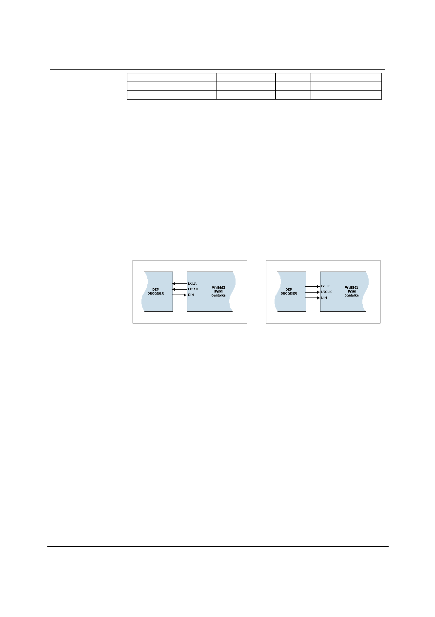
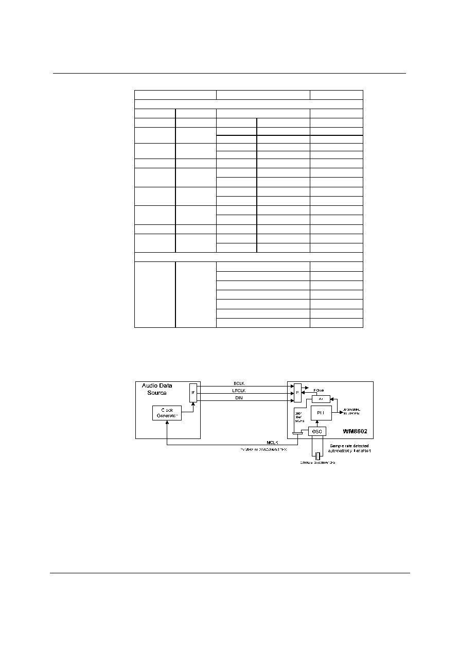
Figure 14 Clock and Audio IF: Clock Master / Audio IF Slave (Default)
Product Preview
WM8602
w
PP Rev 1.5 May 2004
21
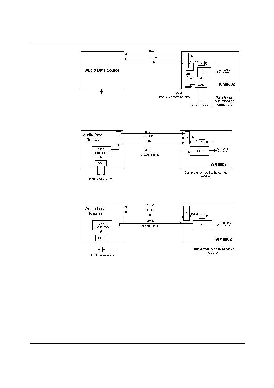
Figure 15 Clock and Audio IF: Clock Master / Audio IF Master
Figure 16 Clock and Audio IF: Clock Slave / Audio IF Slave
Figure 17 Clock and Audio IF: Clock Slave / Audio IF Master
WM8602
Product Preview
w
PP Rev 1.5 May 2004
22
SYNCHRONISER
The WM8602 contains a synchroniser circuit to support the synchronisation of an external LRCLK to
the local LRCLK. This mode is only supported in MPEG mode.
The specification of the synchroniser circuit is:
Test Conditions
AVDD, DVDD, BVDD = 3.3V, AGND, DGND, BGND = 0V, T
A
= +25
o
C, f
XIN
= 27MHz, Slave Mode, fs = 48kHz, 24-bit data,
unless otherwise stated.
PARAMETER
SYMBOL
MIN
TYP
MAX
UNIT
Lock time
t
lock
<1
2
s
LRCLK frequency offset
f
offLRCLK
±1000
±10'000
ppm f
s
0.2
ppm/s
LRCLK drift in Lock
drift
LRCLK
6
Hz
Table 15 Synchroniser Specification
REGISTER
ADDRESS
BIT
LABEL
DEFAULT
DESCRIPTION
0
SYNCEN
1
Synchroniser Enable
0: Disable
1: Enable (in MPEG mode only)
2:1
GMIN[1:0]
10
Minimum Synchroniser Gain
00: minimum gain = 2
0
01: minimum gain = 2
1
10: minimum gain = 2
2
11: minimum gain = 2
3
4:3
GMAX[1:0]
10
Maximum Synchroniser Gain
00: maximum gain = 2
8
01: maximum gain = 2
10
10: maximum gain = 2
12
11: maximum gain = 2
14
R32 (20h)
Synchroniser
(1)
5
HOLD
0
Hold Synchroniser (and SR detect)
1 : Synchroniser in hold mode
Table 16 Synchroniser (1)
REGISTER
ADDRESS
BIT
LABEL
DEFAULT
DESCRIPTION
R33 (21h)
Synchroniser
(2)
2:0
SYNTO[2:0]
100
Synchroniser Gain time-out
000: 0.2 ms
001: 0.5 ms
010: 1 ms
011: 2 ms
100: 5 ms (default)
101: 10 ms
110: 20 ms
111: 50 ms
Table 17 Synchroniser (2)
The next table illustrates recommendation for the Synchroniser loop gain G (see also Table 16) and
time-out time (Table 17) with respect to the LRCLK frequency and the resulting Synchroniser lock
time.
Product Preview
WM8602
w
PP Rev 1.5 May 2004
23
G
F
OFFLRCLK
[ppm]
max
min
GAIN TIME-OUT
[ms]
±100
2
8
2
0
~1
±1000
2
10
2
0
~4
±10'000
2
10
2
0
~20
Table 18 Synchroniser Setup and Locking
Note: The Synchroniser requires a continuously running LRCLK. If that is not the case the HOLD
signal has to be applied to avoid the synchronizer drifting.
CONTROL INTERFACE OPERATION
SELECTION OF CONTROL MODE
The WM8602 is controlled by writing to registers through a serial control interface. A control word
consists of 16 bits. The first 7 bits (B15 to B9) are address bits that select which control register is
accessed. The remaining 9 bits (B8 to B0) are register bits, corresponding to the 9 bits in each
control register. The control interface can operate as either a 3-wire or 2-wire MPU interface. The
MODE pin selects the interface format. An internal pull-down resistor configures the Control Interface
to a default 2 wire format.
MODE
INTERFACE FORMAT
Low
2 wire (default)
High
3 wire
Table 19 Control Interface Mode Selection
The WM8606 Control Interface operates as a slave device only.
3-WIRE (SPI COMPATIBLE) SERIAL CONTROL MODE
The WM8602 is controlled using a 3-wire serial interface. SDIN is used for the program data, SCLK
is used to clock in the program data and CSB is use to latch in the program data. The 3-wire
interface protocol is shown in Figure 13.
CSB
SCLK
SDIN
B15
B6
B7
B8
B9
B10
B11
B12
B13
B14
B1
B2
B3
B4
B5
B0
Figure 18 3-wire Serial Interface
The bits B[15:9] are Control Address Bits and the bits B[8:0] are Control Data Bits
2-WIRE SERIAL CONTROL MODE
The WM8602 supports software control via a 2-wire serial bus. Many devices can be controlled by
the same bus, and each device has a unique 7-bit address (this is not the same as the 7-bit address
of each register in the WM8602).
The controller indicates the start of data transfer with a high to low transition on SDIN while SCLK
remains high. This indicates that a device address and data will follow. All devices on the 2-wire bus
respond to the start condition and shift in the next eight bits on SDIN (7-bit address + Read/Write bit,
MSB first). If the device address received matches the address of the WM8602 and the R/W bit is `0',
indicating a write, then the WM8602 responds by pulling SDIN low on the next clock pulse (ACK). If
the address is not recognised or the R/W bit is `1', the WM8602 returns to the idle condition and wait
for a new start condition and valid address.
WM8602
Product Preview
w
PP Rev 1.5 May 2004
24
Once the WM8602 has acknowledged a correct address, the controller sends the first byte of control
data (B15 to B8, i.e. the WM8602 register address plus the first bit of register data). The WM8602
then acknowledges the first data byte by pulling SDIN low for one clock pulse. The controller then
sends the second byte of control data (B7 to B0, i.e. the remaining 8 bits of register data), and the
WM8602 acknowledges again by pulling SDIN low.
The transfer of data is complete when there is a low to high transition on SDIN while SCLK is high.
After receiving a complete address and data sequence the WM8602 returns to the idle state and
waits for another start condition. If a start or stop condition is detected out of sequence at any point
during data transfer (i.e. SDIN changes while SCLK is high), the device jumps to the idle condition.
SDIN
SCLK
register address and
1st register data bit
DEVICE ADDRESS
(7 BITS)
RD / WR
BIT
ACK
(LOW)
CONTROL BYTE 1
(BITS 15 TO 8)
CONTROL BYTE 1
(BITS 7 TO 0)
remaining 8 bits of
register data
STOP
START
ACK
(LOW)
ACK
(LOW)
Figure 18 2-Wire Serial Control Interface
The WM8602 has two possible device addresses, which can be selected using the CSB pin.
CSB STATE
DEVICE ADDRESS
Low
0011010
High
0011011
Table 20 2-Wire MPU Interface Address Selection
INPUT PROCESSOR
The WM8602 supports the production of stereo or 2.1 outputs from stereo inputs according to Table
21.
OUTPUT CONFIGURATIONS
CONFIG
FL OUT
FR OUT
SUB
OUT
Stereo
·
·
2.1
·
·
·
Table 21 Output Configuration
Product Preview
WM8602
w
PP Rev 1.5 May 2004
25
REGISTER
ADDRESS
BIT
LABEL
DEFAULT
DESCRIPTION
R3 (03h)
Input/Output
Configuration
3
OPCFG[1:0]
1
Output Configuration
0 = Stereo
1 = 2.1
Table 22 Input and Output Configuration Register
The WM8602 also supports Stereo input Stereo output via the Bass Management filtering
options, as discussed in Bass Management (page 25). In this case, the output configuration is
set to 2.1.
Where there are a different number of input and output channels, the data is processed as follows.
Refer to the section on Bass Management (page 25) for details on how the sub-channel is created.
STEREO INPUT STEREO OUTPUT
The Left and Right inputs are passed to the Left and Right Outputs. All other channels are muted.
STEREO INPUT 2.1 OUTPUT
The Left and Right inputs are passed to the Left and Right outputs. The low-frequency contents of
the Left and Right inputs, may be optionally mixed and passed to the SUB output.
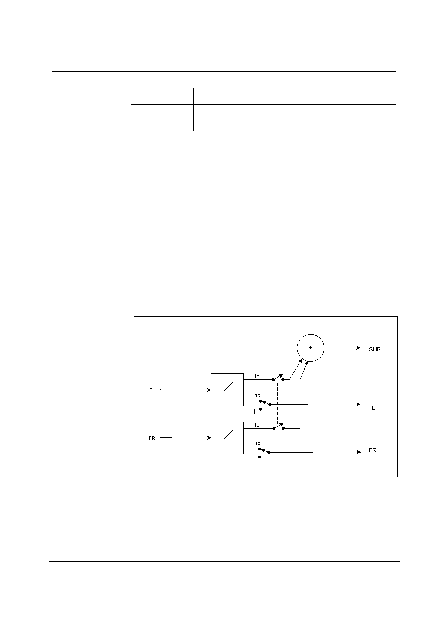
BASS MANAGEMENT
The Bass-Management function filters and combines the input signals to produce a low-pass filtered
output for the sub-woofer channel and high-pass filtered outputs for the remaining channels. The
filters have selectable cut-off frequencies to match different types of sub-woofer and satellite
speakers. The filters are designed so that the cut-off frequencies for the high-pass and low-pass
filters remain constant irrespective of the sampling frequency used. 1
st
order filters are used for the
low-pass and high-pass filters.
Figure 19 Bass Management
The high-pass filters pairs can be bypassed to allow full-range speakers to be used on the main
output pair.
The Bass-Management also provides a selectable LFE boost of 10dB via the LFEBOOST control bit.
Additional gain-adjust is provided after this block (refer to Digital Volume Control, page 28).
WM8602
Product Preview
w
PP Rev 1.5 May 2004
26
REGISTER
ADDRESS
BIT
LABEL
DEFAULT
DESCRIPTION
1:0
LPHPCO[1:0]
01
Low-/High-Pass Cutoff Frequency (-3dB)
00 = 75Hz
01 = 100Hz
10 = 133Hz
11 = 178Hz
R13 (0Dh)
Bass
Management
Filter
2
LFEBOOST
0
LFE Boost Enable
0 = Boost Disabled
1 = 10dB Boost Enabled
Table 23 Bass Management Filter
REGISTER
ADDRESS
BIT
LABEL
DEFAULT
DESCRIPTION
R14 (0Eh)
Bass
Management
0
HPENF
1
Left/Right High-Pass Filter
0 = High-Pass Filter bypassed
1 = High-Pass Filter enabled
Filter Bypass
3
LPENF
1
Left/Right Low-Pass Filter Enable
0 = Low-Pass Filter output disabled
1 = Low-Pass Filter output enabled
Table 24 Bass Management Filter Bypass
GRAPHIC EQUALISER
The WM8602 has a 4-band Graphic Equaliser on the main channels. The three upper bands are
controlled via registers (see Table 25, Table 26, Table 27 and Table 28). The lowest band is
controlled via the subwoofer volume control (see VOLS in Table 31). The function has selectable cut-
off frequencies which are independent of sample rate. The boost/cut for the upper three bands is
controllable in 1.5dB steps from -6dB to +9dB via the EQB control bits.
REGISTER
ADDRESS
BIT
LABEL
DEFAULT
DESCRIPTION
R15 (0Fh)
EQ Band 1
Gain Control
3:0
EQ1GF
[3:0]
1111
(Disabled)
Band 1 Left/Right Gain
0000 or 0001 = +9dB
0010 = +7.5dB
... (1.5dB steps)
1011 to 1110 = -6dB
1111 = Disable
Table 25 EQ Band 1 Gain Control
REGISTER
ADDRESS
BIT
LABEL
DEFAULT
DESCRIPTION
R16 (10h)
EQ Band 2
Gain Control
3:0
EQ2GF
[3:0]
1111
(Disabled)
Band 2 Left/Right Gain
0000 or 0001 = +9dB
0010 = +7.5dB
... (1.5dB steps)
1011 to 1110 = -6dB
1111 = Disable
Table 26 EQ Band 2 Gain Control
Product Preview
WM8602
w
PP Rev 1.5 May 2004
27
REGISTER
ADDRESS
BIT
LABEL
DEFAULT
DESCRIPTION
R17 (11h)
EQ Band 3
Gain Control
3:0
EQ3GF
[3:0]
1111
(Disabled)
Band 3 Left/Right Gain
0000 or 0001 = +9dB
0010 = +7.5dB
... (1.5dB steps)
1011 to 1110 = -6dB
1111 = Disable
Table 27 EQ Band 3 Gain Control
REGISTER
ADDRESS
BIT
LABEL
DEFAULT
DESCRIPTION
0
EQ1CF
1
Band 1 Left/Right Centre-Frequency
0 = High Cutoff (500Hz)
1 = Low Cutoff (250Hz)
2
EQ2CF
1
Band 2 Left/Right Centre-Frequency
0 = High Cutoff (2kHz)
1 = Low Cutoff (1kHz)
R18 (12h)
EQ Centre-
Frequency
Control
4
EQ3CF
1
Band 3 Left/Right Cutoff Frequency
0 = High Cutoff (8kHz)
1 = Low Cutoff (4kHz)
Table 28 EQ Frequency Control
Band 0 is controlled via the sub-woofer volume control register R11 as described in Table 31. The
functionality to add/subtract the boost/cut setting to the sub-woofer volume must be written into the
software controller for the chip.
The Band 0 Cutoff frequency can be changed using the corner frequency of the low-pass/high-pass
filters as described in Table 23.
DIGITAL LOUDSPEAKER EQUALISER
A loudspeaker equaliser is provided to compensate for high-frequency variations that can occur when
loudspeakers of different impedances are used with different output filters in typical output stages.
The equaliser has selectable cut-off frequencies which are independent of sample rate. The gain at
20kHz is controllable in 0.5dB steps from -1.5dB to +2dB via the LSEQ control bit. The settings are
applied to Left and Right channels simultaneously.
REGISTER
ADDRESS
BIT
LABEL
DEFAULT
DESCRIPTION
0
LSCO
0
LSEQ Filter Characteristic
0 = High Cutoff (15kHz)
1 = Low Cutoff (10kHz)
R19 (13h)
Loudspeaker
Equaliser
3:1
LSEQ
[2:0]
100
(Disabled)
High Frequency Equalisation
000 = +2dB
001 = +1.5dB
010 = +1dB
011 = +0.5dB
100 = Disable
101 = -0.5dB
110 = -1dB
111 = -1.5dB
Table 29 Loudspeaker Equaliser

WM8602
Product Preview
w
PP Rev 1.5 May 2004
28
DIGITAL DEEMPHASIS
The digital `de-emphasis' is used to equalize pre-emphasised digital CD recordings. De-emphasis
filtering is available on the Left and Right channels only, for sample rates of 32kHz, 44.1kHz and
48kHz. The settings are applied to the two channels simultaneously.
REGISTER
ADDRESS
BIT
LABEL
DEFAULT
DESCRIPTION
R20 (14h)
De-emphasis
0
DEEMP
0
De-emphasis Control
0 = No De-emphasis
1 = De-emphasis enabled
Table 30 De-emphasis
Refer to Figure 30, Figure 31, Figure 32, Figure 33, Figure 34 and Figure 35 for details of the De-
Emphasis modes at different sample rates.
Note: Using the De-emphasis filters for other sample rates as defined above will result in a frequency
response error as shown in Figure 31, Figure 33 and Figure 35.
DIGITAL VOLUME CONTROL
The volume control allows the gain of each channel to be independently adjusted in 0.5dB steps from
-103.5dB to +24dB. When the Dynamic Peak Compressor (see below) is enabled, gains of greater
than 0dB can be applied without digital clipping occurring. The volume control has a digital zero-cross
circuit which minimises clicks during changing the volume.
An update control bit is provided which allows the volume setting on each channel to be first stored in
an intermediate latch, then afterwards applied simultaneously to all channels. If UPDATE=0, the
Volume value will be written to the pre-latch but not applied to the relevant channel. If UPDATE=1, all
pre-latched values will be applied from the next input sample. The value of UPDATE itself is not
latched.
To prevent audible clicks, the volume control includes a ramp function which automatically ramps the
volume in small steps between register updates. The ramp rate is 256dB/s ±5%.
REGISTER
ADDRESS
BIT
LABEL
DEFAULT
DESCRIPTION
7:0
VOLL[7:0]
10110001
(-15dB)
Left Volume in 0.5dB steps. Refer to
Table 14
R4 (04h)
Left Volume
8
UPDATE
0
Volume Update
0 = Store LVOL in intermediate latch
(no gain change)
1 = Store and Update all channel
gains
7:0
VOLR [7:0]
10110001
(-15dB)
Right Volume in 0.5dB steps. Refer to
Table 14
R5 (05h)
Right Volume
8
UPDATE
0
Volume Update
0 = Store RVOL in intermediate latch
(no gain change)
1 = Store and Update all channel
gains
7:0
VOLS [7:0]
10110001
(-15dB)
Sub Volume in 0.5dB steps. Refer to
Table 14
R10 (0Ah)
Subwoofer
Volume
8
UPDATE
0
UPDATE
0 = Store SVOL in intermediate latch
(no gain change)
1 = Store and Update all channel
gains
Table 31 Volume Control
Product Preview
WM8602
w
PP Rev 1.5 May 2004
29
VOLXX[7:0]
VOLUME LEVEL
00(hex)
-dB (mute)
01(hex)
-103dB
:
:
:
:
CF(hex)
0dB
:
:
:
:
FE(hex)
+23.5dB
FF(hex)
+24dB
Table 32 Volume Control Levels
DUAL VOLUME CONTROL
Setting the DVC register bit causes the volume settings to be applied in pairs. For example, the
DVCF causes the Left channel volume settings to be applied to both the Left and Right channels
from the next audio input sample. No update to the VOL registers is required for DVC to take effect.
REGISTER
ADDRESS
BIT
LABEL
DEFAULT
DESCRIPTION
R11 (0Bh)
Dual Volume
Control
0
DVCF
0
Dual Volume Control Left/Right
Channels:
0 : Use VOLFR setting for Right
channel
1: Apply VOLFL setting to Right
channel
Table 33 Dual Volume Control
SOFT MUTE AND AUTO-MUTE
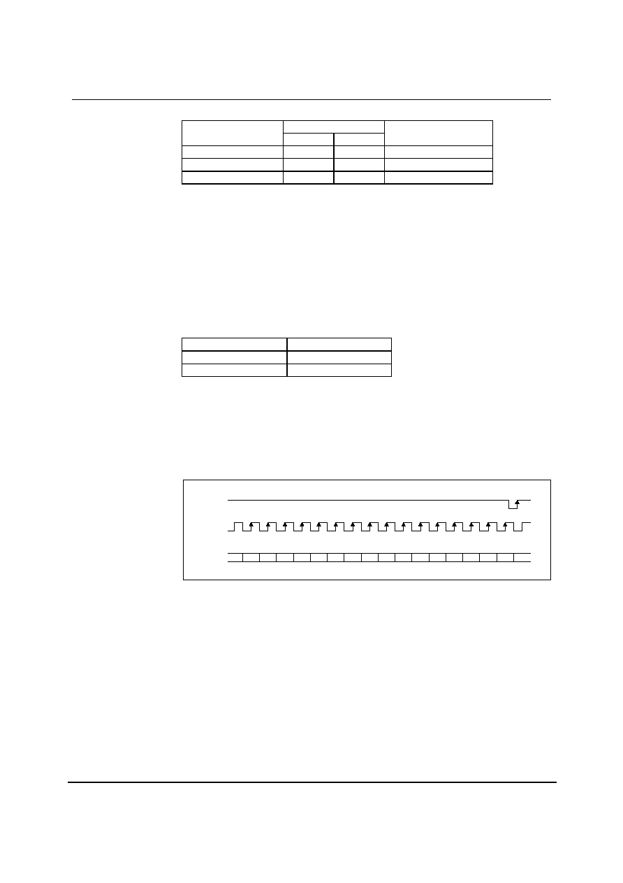
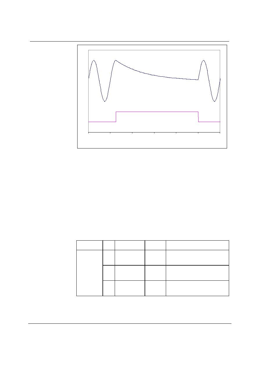
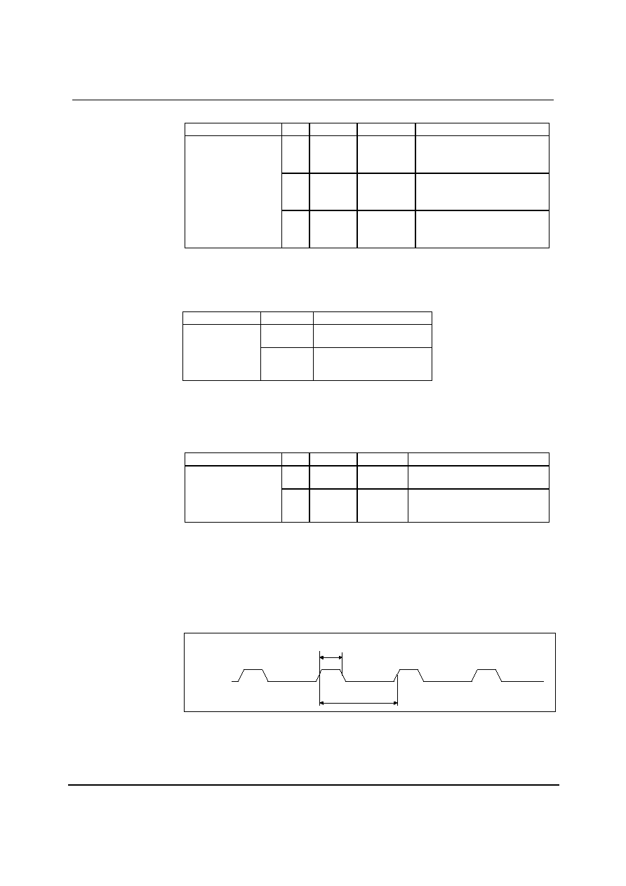
The WM8602 has a Soft Mute function set by the SMUTE control bit. Figure 20 shows the application
and release of SMUTE while a full amplitude sinusoid is being played at 48kHz sampling rate. When
SMUTE (lower trace) is asserted, the output (upper trace) begins to decay exponentially from the DC
level of the last input sample. The output will decay towards zero with a time constant of
approximately 64 input samples. When SMUTE is turned off, the output will restart almost
immediately from the current input sample, thus possibly causing a pop sound.
This function is disabled by default.
WM8602
Product Preview
w
PP Rev 1.5 May 2004
30
Figure 20 Application and Release of Soft Mute
An auto-mute function is provided which automatically mutes the output stage when a digital silence
period is detected. Digital silence is defined as a consecutive period of 1024 zero input samples at
the output of the volume control. Auto-mute will be removed as soon as the volume control output
becomes non-zero. (Please note that on the sub channel the noise level is greatly reduced, rather
than complete digital silence.)
To achieve digital silence, you can do one of the following:
·
Turn on auto-mute and set the volume control to zero.
·
Turn on auto-mute and input zero data on the serial data input pins with the bass
management filters disabled. (Page 25)
·
Turn on auto-mute and soft mute.
The auto-mute operates independently for Left/Right and Subwoofer channels and can be enabled or
disabled separately.
The mute features maximize the SNR of the PWM amplifier system. Soft-mute will only maximize the
SNR for Left/Right or Subwoofer channels if enabled.
REGISTER
ADDRESS
BIT
LABEL
DEFAULT
DESCRIPTION
0
SMUTE
0
Digital Soft Mute
0 = disable (signal active)
1= enable
1
AMUTEF
1
Left/Right Auto-mute
0 = disable
1 = enable
R12 (0Ch)
Mute
4
AMUTESB
1
Subwoofer Auto-mute
0 = disable
1 = enable
Table 34 Mute
-2.5
-2
-1.5
-1
-0.5
0
0.5
1
1.5
0
0.001
0.002
0.003
0.004
0.005
0.006
Time(s)
Product Preview
WM8602
w
PP Rev 1.5 May 2004
31
DYNAMIC PEAK COMPRESSOR
The WM8602 includes a Dynamic Peak Compressor for each channel, which prevents the
occurrence of digital clipping when gains in excess of 0dB are applied. The compressor automatically
adjusts the signal amplitude to allow headroom for the LFE boost, sub-woofer mixing, tone controls,
loudspeaker equalisation and digital volume control. The compressor has a programmable limit
threshold, programmable attack and decay time-constants, a frequency-dependent decay mode, and
built-in zero-cross detect. The compressor can be configured either to operate independently on all
channels (DUAL MONO), or on linked channel-pairs (STEREO).
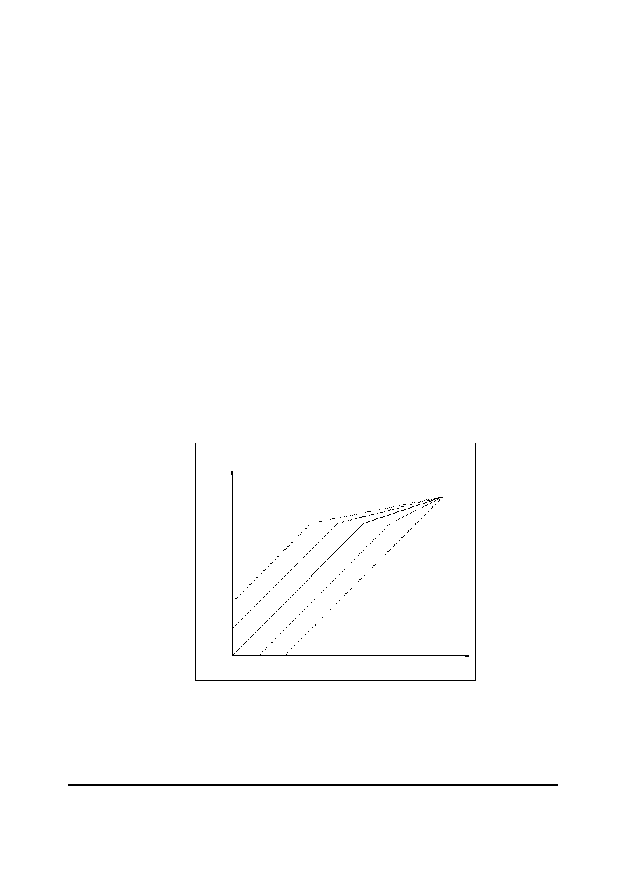
COMPRESSOR THRESHOLD
The compressor has a digital peak detector which tracks the maximum input signal level at the
output of the volume control. With reference to Figure 21, if this signal is below the threshold set by
control bit THRESH, the compressor operates transparently with no change to the signal level.
However, if peak signal rises above the threshold, the gain through the compressor is modified so
that the upper part of the curve is followed. This ensures that the output signal does not exceed 0dB.
ATTACK AND DECAY TIMES
The attack time-constant ATK controls how fast the gain is reduced when the signal goes above the
threshold. It is defined as the time taken for the gain to reduce by 6dB. Normally a short attack time-
constant is used to prevent the signal clipping when a high-amplitude transient occurs.
The decay time-constant DCY controls how fast the gain is increased when the signal begins to fall
again. It is defined as the time taken for the gain to increase by 6dB. Normally, the decay time-
constant is much longer than the attack time-constant, to prevent the input signal from entering
repeated limiting cycles.
The frequency-dependent decay feature automatically detects the input frequency and sets the
decay time to decay slower for low frequency signals. This reduces low-frequency signal distortion by
preserving the waveform of each input cycle, whilst allowing the compressor to respond quickly to
high frequency transients. This feature is enabled via the FDEP control bit.
0dB
Output Level
(dB)
Peak Input Level [dB]
THRESH
[dB]
0
-6
-12
+6
+12
-18
-24
-30
-36
-12
-18
-24
-30
-36
0dB
-6dB
-12dB
+6dB
+12dB
typical
Volume Control
Setting
Figure 21 Dynamic Peak Compressor Characteristics

WM8602
Product Preview
w
PP Rev 1.5 May 2004
32
REGISTER
ADDRESS
BIT
LABEL
DEFAULT
DESCRIPTION
R21 (15h)
Left/Right
Channels
Dynamic
Peak
Compressor
0
PLENF
1
Left/Right Channel Compressor
Enable
0 = disable
1 = enable
Table 35 Left/Right Channel Dynamic Peak Compressor (1)
REGISTER
ADDRESS
BIT
LABEL
DEFAULT
DESCRIPTION
2:0
ATK[2:0]
010
Left/Right Channel Attack Rate
000 = 170µs
001 = 330µs
010 = 670µs
011 = 1.33ms
100 = 2.67ms
101 = 5.33ms
110 = 10.7ms
111 = 20.1ms
5:3
DCY[2:0]
011
Left/Right Channel Decay Rate
000 = 340ms
001 = 680ms
010 = 1.36s
011 = 2.73s
100 = 5,46s
101, 110, 111 = 10.9s
7:6
THRESH[1:0]
11
Left/Right Channel Compressor
Thresholds
00 = -12dB
01 = -9dB
10 = -6dB
11 = -3dB
R22 (16h)
Left/Right
Channels
Dynamic
Peak
Compressor
8
FDEP
0
Frequency-dependent decay
0 = disable
1 = enable
Table 36 Left/Right Channel Dynamic Peak Compressor (2)
REGISTER
ADDRESS
BIT
LABEL
DEFAULT
DESCRIPTION
R23 (17h)
Sub Channel
Dynamic
Peak
Compressor
0
PLENSUB
1
Sub Channel Compressor Enable
0 = disable
1 = enable
Table 37 Subwoofer Channel Dynamic Peak Compressor (1)

Product Preview
WM8602
w
PP Rev 1.5 May 2004
33
REGISTER
ADDRESS
BIT
LABEL
DEFAULT
DESCRIPTION
2:0
ATK[2:0]
010
Sub Channel Attack Rate
000 = 170µs
001 = 330µs
010 = 670µs
011 = 1.33ms
100 = 2.67ms
101 = 5.33ms
110 = 10.7ms
111 = 20.1ms
5:3
DCY[2:0]
011
Sub Channel Decay Rate
000 = 340ms
001 = 680ms
010 = 1.36s
011 = 2.73s
100 = 5,46s
101, 110, 111 = 10.9s
7:6
THRESH[1:0]
11
Sub Channel Compressor Thresholds
00 = -12dB
01 = -9dB
10 = -6dB
11 = -3dB
R24 (18h)
Sub Channel
Dynamic
Peak
Compressor
8
FDEP
0
Frequency-dependent decay
0 = disable
1 = enable
Table 38 Subwoofer Channel Dynamic Peak Compressor (2)
ZERO-CROSS DETECT
The Dynamic Peak Compressor has a zero-cross detect which minimises clicks during gain changes.
The zero-cross detect can be enabled/disabled for Left/Right or Subwoofer channels. The zero-cross
has a timeout feature which ensures that the volume will change even if the input has a large DC
offset. Once a new gain has been requested from the Dynamic Peak Compressor, the zero-cross
detector will wait for a zero-cross for 25 to 50
ms before applying the gain change.
REGISTER
ADDRESS
BIT
LABEL
DEFAULT
DESCRIPTION
0
ZCF
1
Zero-Cross Enable Left/Right
Channels:
0 : Disable Zero-Cross
1: Enable Zero-Cross
3
ZCSUB
1
Zero-Cross Enable Sub Channel:
0 : Disable Zero-Cross
1: Enable Zero-Cross
R25 (19h)
Volume
Control Zero-
Cross
4
ZCT
1
Zero Cross Timeout Enable:
0 : Disable Zero-Cross Timeout
1: Enable Zero-Cross Timeout
Table 39 Volume Control Zero-Cross
WM8602
Product Preview
w
PP Rev 1.5 May 2004
34
INTERPOLATION FILTERS
The WM8602 uses two types of interpolation filters, selected according to sampling frequency, as
shown in Table 39.
SAMPLING FREQUENCY
FILTER TYPE
INTERPOLATION
Main Channels
Main Channels
SUB
32kHz
0
12x
6x
44.1kHz
0
8x
4x
48kHz
0
8x
4x
88.2kHz
0
4x
2x
96kHz
0
4x
2x
176.4kHz
1
2x
1x
192kHz
1
2x
1x
Table 40 Interpolation Filter Types
FILTER TYPE 0
PARAMETER
SYMBOL
TEST CONDITIONS
MIN
TYP
MAX
UNIT
Filter
Passband
±0.05 dB
0.454
f
s
Stopband
-3dB
0.484
f
s
Passband ripple
±0.05
dB
Stopband Attenuation
f > 0.546fs
-60
dB
Group Delay
23
samples
Table 41 Digital Filter 0 Characteristics
FILTER TYPE 1
PARAMETER
SYMBOL
TEST CONDITIONS
MIN
TYP
MAX
UNIT
Filter
Passband
0.242
f
s
Stopband
0.723
f
s
Passband ripple
±0.05
dB
Stopband Attenuation
-60
dB
Group Delay
6
samples
Table 42 Digital Filter 1 Characteristics
The subwoofer filter characteristic is defined in table
FILTER TYPE SUBWOOFER
PARAMETER
SYMBOL
TEST CONDITIONS
-0.1dB
-3dB
UNIT
Sample Rate
32k
2.0
10.7
kHz
44k1
2.7
14.5
kHz
48k
3.0
15.8
kHz
88k2
6.1
32.1
kHz
96k
6.8
34.9
kHz
176k
*
*
kHz
192k
*
*
kHz
Table 43 Subwoofer Filter Characteristic
Note: * indicates no interpolation filters
Product Preview
WM8602
w
PP Rev 1.5 May 2004
35
PCM TO PWM CONVERTER
The PCM to PWM converter converters the Pulse-Code Modulated (PCM) signal into a highly linear
Pulse-Width Modulated (PWM) signal. Table 44 defines the Pulse Repetition Frequency, (PRF),
output clock rate (OBCLK) and minimum pulse width for each supported sampling frequency.
t
PWMP
t
PWMP
t
PWMM
t
PWMM
t
OBCLK
Figure 22 PCM to PWM Converter
The PRF Frequency (T
PWMP
) of the Sub-woofer channel is half of the frequency defined in Table 44
in order to reduce power dissipation in the output stage.
PRF
(1/T
PWMP
)
Main Channel
SUB
OUTPUT BITCLOCK
FREQUENCY
(1/T
OBCLK
)
MINIMUM PULSE
WIDTH (T
PWMM
)
SAMPLING
FREQUENCY
[kHz]
[kHz]
[MHz]
[ns]
32kHz
384
192
98.304
122
44.1kHz
352.8
176.4
90.3168
133
48kHz
384
192
98.304
122
88.2kHz
352.8
176.4
90.3168
133
96kHz
384
192
98.304
122
176.4kHz
352.8
176.4
90.3168
133
192kHz
384
192
98.304
122
Table 44 Output Bitclock Frequency
Notes:
1. The correct Output Bitclock Frequency (T
OBCLK
) is generated by the built-in PLL of the WM8602
device. The incoming clock must meet the jitter specification defined in Table 3.
OUTPUT PHASE
The Phase control word determines whether the output of each channel is non-inverted or inverted.
REGISTER
ADDRESS
BIT
LABEL
DEFAULT
DESCRIPTION
Bit
Channel
Phase
0
L
1 = invert
1
R
1 = invert
R26 (1Ah)
Output Phase
6:0
PH[6:0]
0000000
6
SUB
1 = invert
Table 45 Phase
WM8602
Product Preview
w
PP Rev 1.5 May 2004
36
PWM OUTPUT CONFIGURATION
The PWM output format can be defined with the PWMCFG setting defined in Table 46.
REGISTER
ADDRESS
BIT
LABEL
DEFAULT
DESCRIPTION
2:1
PWMCFG
[1:0]
00
PWM Output State when output disabled
or in standby mode:
01 = all PWM Outputs high
00 = all PWM Outputs low
10, 11 = high impedance
3
PWMPH
1
PWM Output Phase
0 = PWM outputs in phase
1 = PWM outputs phase shifted to each
other
R27 (1Bh)
PWM Output
Configuration
7
PWMCLK
0
PWM Output Clock
0 = disabled
1 = enabled
Table 46 PWM Output Configuration
OUTPUT CONFIGURATION
If required the WM8602 device can be disabled in a system by setting the TRI bit as defined in Table
47. Setting the TRI bit will set all output pins of the device to high impedance.
REGISTER
ADDRESS
BIT
LABEL
DEFAULT
DESCRIPTION
R28 (1Ch)
Output
Configuration
0
TRI
0
Output Pins Mode
0 = Normal
1 = High Impedance
Table 47 Output Configuration
STANDBY, OUTPUT DISABLE AND RESET MODES
STANDBY
Setting the STDBY register bit selects a low power mode, and immediately configures the output to
produce an output defined in Table 46 (PWMCFG). All trace of the previous input samples is
removed, but all control register settings are preserved.
OUTPUT DISABLE (OPDIS) PIN AND REGISTER (OPDISR)
The OPDIS pin is provided to immediately shutdown the outputs, primarily for their protection. This is
useful for short-circuit or thermal protection. The OPDIS pin can be configured in 2 modes:
·
Synchronous
·
Latched
In synchronous mode if OPDIS is high for longer than 100ns the outputs will be disabled. They will be
enabled again at the end of a processing frame when OPDIS goes low for longer than 100ns.
In latched mode if OPDIS is high for longer than 100ns, the outputs will be disabled and will remain
off until OPDIS is reset via the control interface and the end of a processing frame is reached (Table
49).
The output disable register (OPDISR) also allows the PWM outputs to be disabled via a register
write. If OPDISR is set the PWM outputs will be disabled at the end of the next processing frame and
enabled if OPDISR is reset at the end of the next processing frame.
Product Preview
WM8602
w
PP Rev 1.5 May 2004
37
REGISTER ADDRESS
BIT
LABEL
DEFAULT
DESCRIPTION
0
STDBY
1
Standby select:
0 : Normal Mode
1: Standby Mode
1
OPDISR
0
Output disable register
0: Normal mode
1: PWM output disabled
R29 (1Dh)
Power Down
2
MENA
1
OPDIS Mode
0 : Synchronous
1: Latched, reset via Control I/F
Table 48 Power Down
EXTERNAL APPLICATION POWER-DOWN (EAPDB) PIN
The state of the output pin EAPDB shows whether the device is disabled (i.e. OPDIS input pin active
or STDBY register set).
EAPDB
STATE
DESCRIPTION
1
The device is operating
correctly
External
Application
Power Down
0
(default)
The outputs are disabled or
the WM8602 device is in
Standby (default) mode
Table 49 EAPDB Pin
RESET
The WM8602 device can be reset writing to the Reset register as defined in Table 50.
REGISTER ADDRESS
BIT
LABEL
DEFAULT
DESCRIPTION
0
RLENA
0
Writing 1 to bit 0 of the register will
reset OPDIS
R30 (1Eh)
Reset
all
RESET
0
Writing all 1's to the register will
reset the device and register
settings
Table 50 Reset
Note: RESET or RLENA will be applied at the end of the register write and released at the beginning
of the next register write. I.e. to reset the OPDIS register write 1 to bit 0 of the Reset register and
them write 0 to bit 0.
EXTERNAL POWER SUPPLY CLOCK
The WM8602 device can generate a clock signal for an external PSU (Power Supply Unit) which is
available at the CLKPSU pin.
CLKPSU
t
PCLKPSU
t
HCLKPSU
Figure 23 External Power Supply Clock

WM8602
Product Preview
w
PP Rev 1.5 May 2004
38
REGISTER
ADDRESS
BIT
LABEL
DEFAULT
DESCRIPTION
0
ENPSU
0
CLKPSU enable
1: enabled
2:1
CLKPSU[1:0]
00
CLKPSU frequency
00: CLKPSU = f
PRF
01: CLKPSU = f
PRF
/2
10: CLKPSU = f
PRF
/4
11: CLKPSU = f
PRF
/6
R31 (1Fh)
PSU
4:3
DCYPSU[1:0]
00
CLKPSU duty cycle
00: t
hclkpsu
/t
pclkpsu
= 0.5 (50%)
01: t
hclkpsu
/t
pclkpsu
= 0.125 (12.5%)
10: t
hclkpsu
/t
pclkpsu
= 0.0625 (6.25%)
11: t
hclkpsu
/t
pclkpsu
= 0.03125 (3.125%)
Table 51 PSU Clock
Note: See Table 44 for specification of f
PRF
.

Product Preview
WM8602
w
PP Rev 1.5 May 2004
39
REGISTER MAP
The complete register map is shown below. The detailed description can be found in the relevant text of the device description.
There are 30 registers with 9 bits per register. These can be controlled using the Control Interface.
REGISTER
ADDRESS
REMARKS
BIT[8]
BIT[7]
BIT[6]
BIT[5]
BIT[4]
BIT[3]
BIT[2]
BIT[1]
BIT[0]
DEFAULT
PAGE REF
R0 (00h)
00_0000
Clocking
0
0
0
0
0
CLKDIV2 MEDGE
MPEG
CMAST 0_0000_0011
19
R1 (01h)
00_0001
Sample Rate
0
0
0
0
SRDET
SR
0_0001_0000
19
R2 (02h)
00_0010
Audio IF Format
BCLKINV
MS
LRSWAP
0
LRP
WL
FORMAT
0_0000_1010
18
R3 (03h)
00_0011
Input/Output Configuration
0
0
0
0
1
OPCFG
0
0
1
0_0001_1001
25
R4 (04h)
00_0100
Left Volume
UPDATE
VOLFL (Left) Volume
0_1011_0001
28
R5 (05h)
00_0101
Right Volume
UPDATE
VOLFR (Right) Volume
0_1011_0001
28
R10 (0Ah)
00_1010
Subwoofer Volume
UPDATE
VOLS (Subwoofer) Volume
0_1011_0001
28
R11 (0Bh)
00_1011
Dual Volume Control
0
0
0
0
0
0
0
0
DVCF
0_0000_0000
29
R12 (0Ch)
00_1100
Mute
0
0
0
0
AMUTESB
1
1
AMUTEF SMUTE 0_0001_1110
30
R13 (0Dh)
00_1101
Bass (1)
0
0
0
0
0
0
LFEBOOST
LPHPCO
0_0000_0001
26
R14 (0Eh)
00_1110
Bass (2)
0
0
0
1
1
LPENF
1
1
HPENF
0_0011_1111
26
R15 (0Fh)
00_1111
EQ Band 1 Gain Control
0
1
1
1
1
EQ1GF
0_1111_1111
26
R16 (10h)
01_0000
EQ Band 2 Gain Control
0
1
1
1
1
EQ2GF
0_1111_1111
26
R17 (11h)
01_0001
EQ Band 3 Gain Control
0
1
1
1
1
EQ3GF
0_1111_1111
27
R18 (12h)
01_0010
EQ Frequency Control
0
0
0
1
EQ3CF
1
EQ2CF
1
EQ1CF
0_0011_1111
27
R19(13h)
01_0011
Speaker Equaliser
0
0
0
0
0
LSEQ
LSCO
0_0000_1000
27
R20 (14h)
01_0100
Deemphasis
0
0
0
0
0
0
0
0
DEEMPH 0_0000_0000
28
R21 (15h)
01_0101
Peak Compressor F (1)
0
0
0
0
0
0
0
0
PLENF
0_0000_0001
32
R22 (16h)
01_0110
Peak Compressor F (2)
FDEP
THRESH
DCY
ATK
0_1101_1010
32
R23 (17h)
01_0111
Peak Compressor SUB (1)
0
0
0
0
0
0
0
0
PLENSUB
0_0000_0001
32
R24 (18h)
01_1000
Peak Compressor SUB (2)
FDEP
THRESH
DCY
ATK
0_1101_1010
33
R25 (19h)
01_1001
Zero Cross
0
0
0
0
ZCT
ZCSUB
1
1
ZCF
0_0001_1111
33
R26 (1Ah)
01_1010
Output phase
0
0
PH
0_0000_0000
35
R27 (1Bh)
01_1011
PWM Output Config
0
PWMCLK
0
0
0
PWMPH
PWMCFG
0
0_0000_1000
36
R28 (1Ch)
01_1100
Output Config
0
0
0
0
0
0
0
0
TRI
0_0000_0000
36
R29 (1Dh)
01_1101
Power Down
0
0
0
0
0
0
MENA
OPDISR
STDBY
0_0000_0101
37
R30 (1Eh)
01_1110
Reset
0
0
0
0
0
0
0
0
RLENA
0_0000_0000
37
R31 (1Fh)
01_1111
PSU
0
0
0
0
DCYPSU
CLKPSU
ENPSU 0_0000_0000
38
R32 (20h)
10_0000
Synchroniser (1)
0
0
0
HOLD
GMAX
GMIN
SYNCEN 0_0001_0101
22
R33 (21h)
10_0001
Synchroniser (2)
0
0
0
0
0
0
SYNTO
0_0000_0100
22
Table 52 Register Map Description
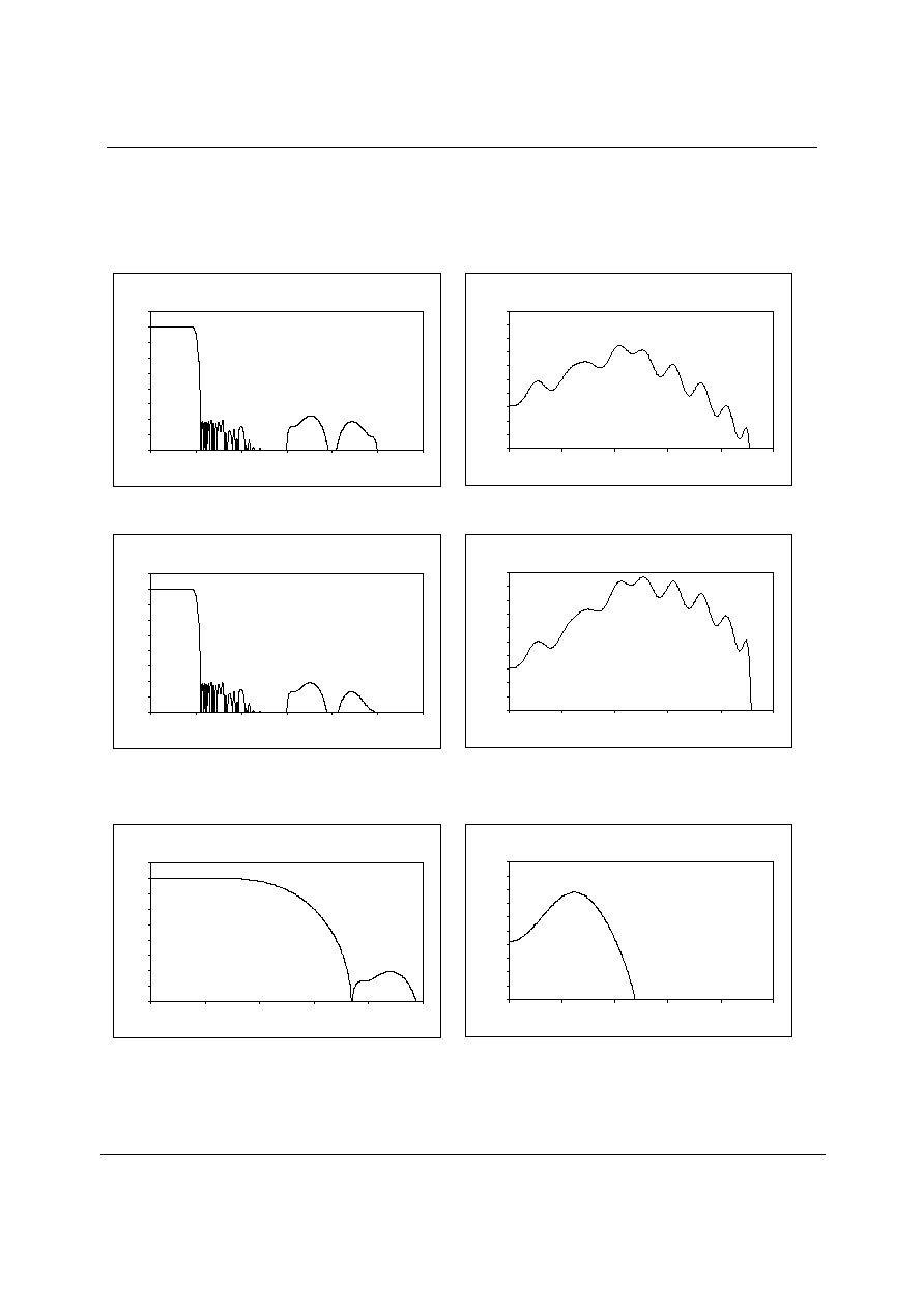
WM8602
Product Preview
w
PP Rev 1.5 May 2004
40
DIGITAL FILTER CHARACTERISTICS
FILTER RESPONSES
-80
-70
-60
-50
-40
-30
-20
-10
0
10
0
0.5
1
1.5
2
2.5
3
Frequency (Fs)
Res
p
ons
e
(dB
)
Figure 24 Digital Filter Frequency Response 32kHz
-0.05
-0.04
-0.03
-0.02
-0.01
0
0.01
0.02
0.03
0.04
0.05
0
0.1
0.2
0.3
0.4
0.5
Frequency (Fs)
Res
pons
e
(dB
)
Figure 25 Digital Filter Ripple 32kHz
-80
-70
-60
-50
-40
-30
-20
-10
0
10
0
0.5
1
1.5
2
2.5
3
Frequency (Fs)
R
e
s
pon
s
e
(
dB
)
Figure 26 Digital Filter Frequency Response 44.1, 48
and 96kHz
-0.05
-0.04
-0.03
-0.02
-0.01
0
0.01
0.02
0.03
0.04
0.05
0
0.1
0.2
0.3
0.4
0.5
Frequency (Fs)
Res
p
ons
e
(dB
)
Figure 27 Digital Filter Ripple 44.1, 48 and 96kHz
-80
-70
-60
-50
-40
-30
-20
-10
0
10
0
0.2
0.4
0.6
0.8
1
Frequency (Fs)
Res
p
ons
e
(dB
)
Figure 28 Digital Filter Frequency Response 176.4kHz
and 192kHz
-0.05
-0.04
-0.03
-0.02
-0.01
0
0.01
0.02
0.03
0.04
0.05
0
0.1
0.2
0.3
0.4
0.5
Frequency (Fs)
Res
pons
e
(dB
)
Figure 29 Digital filter Ripple 176.4kHz and 192kHz
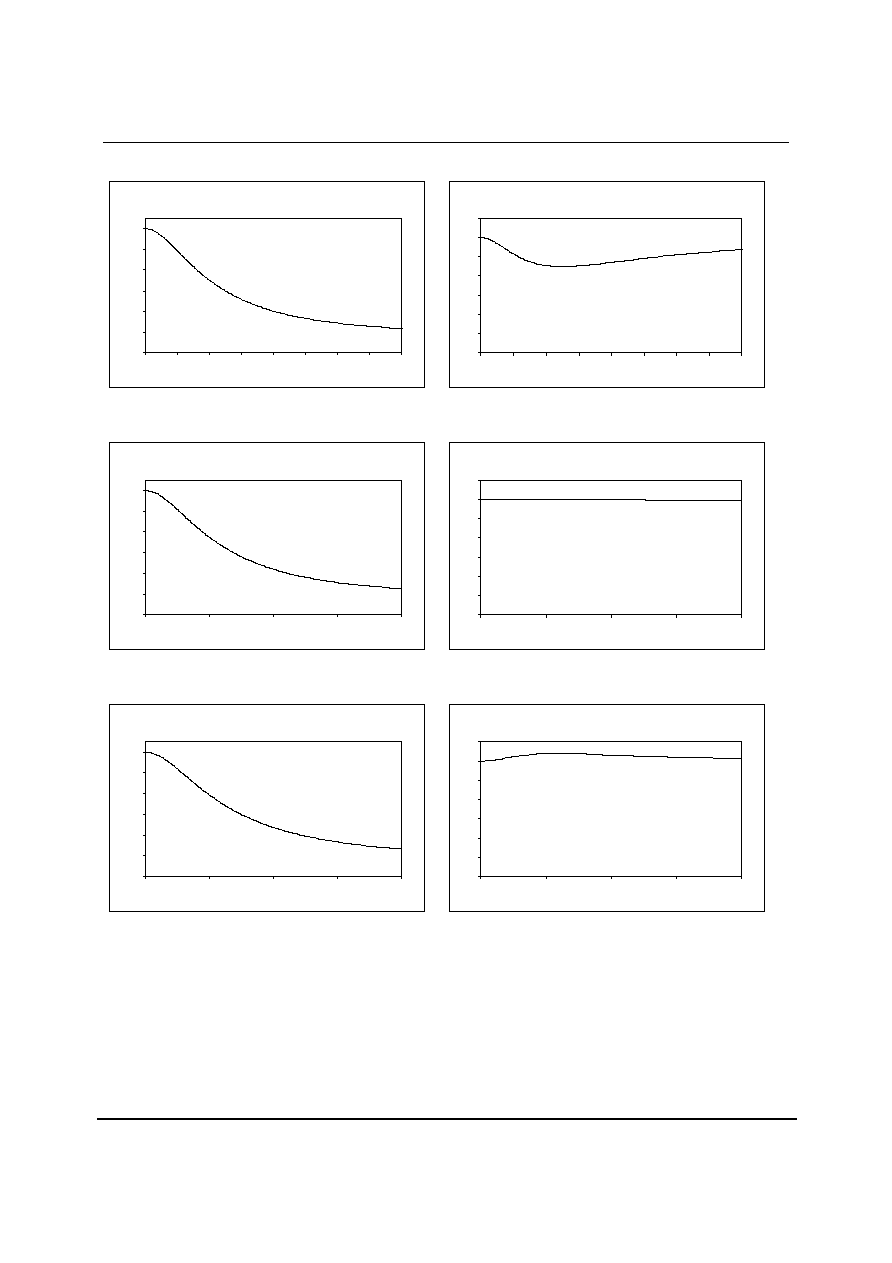
Product Preview
WM8602
w
PP Rev 1.5 May 2004
41
DIGITAL DE-EMPHASIS CHARACTERISTICS
-12
-10
-8
-6
-4
-2
0
0
2000
4000
6000
8000
10000
12000
14000
16000
Frequency (Hz)
R
e
sp
o
n
se
(
d
B
)
Figure 30 De-Emphasis Frequency Response (32kHz)
-6
-5
-4
-3
-2
-1
0
1
0
2000
4000
6000
8000
10000
12000
14000
16000
Frequency (Hz)
R
e
sp
o
n
se
(
d
B
)
Figure 31 De-Emphasis Error (32kHz)
-12
-10
-8
-6
-4
-2
0
0
5000
10000
15000
20000
Frequency (Hz)
R
e
s
p
ons
e
(
dB
)
Figure 32 De-Emphasis Frequency Response (44.1kHz)
-6
-5
-4
-3
-2
-1
0
1
0
5000
10000
15000
20000
Frequency (Hz)
R
e
s
pons
e
(dB
)
Figure 33 De-Emphasis Error (44.1kHz)
-12
-10
-8
-6
-4
-2
0
0
5000
10000
15000
20000
Frequency (Hz)
R
e
s
pons
e
(dB
)
Figure 34 De-Emphasis Frequency Response (48kHz)
-6
-5
-4
-3
-2
-1
0
1
0
5000
10000
15000
20000
Frequency (Hz)
R
e
s
pons
e
(dB
)
Figure 35 De-Emphasis Error (48kHz)
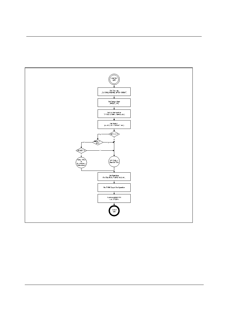
WM8602
Product Preview
w
PP Rev 1.5 May 2004
42
APPLICATION NOTES
START-UP
The WM8602 per default is switched off and the PWM output pins are static high, to protect any
external circuit. When the device has been properly initialized and the output configuration has been
defined then the device can safely be switched on. A typical start-up sequence is show in Figure 36.
Figure 36 WM8602 Start-up

Product Preview
WM8602
w
PP Rev 1.5 May 2004
43
POWER SUPPLY CONNECTIONS
The WM8602 has 3 individual power supplies. Figure 37 shows how these power supplies are
connected and used on the chip and package.
Figure 37 WM8602 Power Supply Connections

WM8602
Product Preview
w
PP Rev 1.5 May 2004
44
APPLICATIONS INFORMATION
RECOMMENDED EXTERNAL COMPONENTS
Figure 38 WM8602 External Component Diagram
RECOMMENDED EXTERNAL COMPONENTS VALUES
COMPONENT REFERENCE
SUGGESTED VALUE
DESCRIPTION
Y1
24.576 / 27.000MHz
Crystal (15pF load, 500
µW)
C1, C2
22pF
Capacitor NP0 0603
C3
4.7µF
Capacitor Y5V 0805
C4-C7
0.1µF
Capacitor X7R 0603
Table 53 External Components Description

Product Preview
WM8602
w
PP Rev 1.5 May 2004
45
PACKAGE DIMENSIONS
NOTES:
A. ALL LINEAR DIMENSIONS ARE IN MILLIMETERS.
B. THIS DRAWING IS SUBJECT TO CHANGE WITHOUT NOTICE.
C. BODY DIMENSIONS DO NOT INCLUDE MOLD FLASH OR PROTRUSION, NOT TO EXCEED 0.20MM.
D. MEETS JEDEC.95 MO-150, VARIATION = AH. REFER TO THIS SPECIFICATION FOR FURTHER DETAILS.
DM007.D
DS: 28 PIN SSOP (10.2 x 5.3 x 1.75 mm)
Symbols
Dimensions
(mm)
MIN
NOM
MAX
A
-----
-----
2.0
A
1
0.05
-----
0.25
A
2
1.65
1.75
1.85
b
0.22
0.30
0.38
c
0.09
-----
0.25
D
9.90
10.20
10.50
e
E
7.40
7.80
8.20
5.00
5.30
5.60
L
0.55
0.75
0.95
A A2
A1
14
1
15
28
E1
E
c
L
GAUGE
PLANE
0.25
e
b
D
SEATING PLANE
-C-
0.10 C
REF:
JEDEC.95, MO-150
E
1
L
1
0.125 REF
0.65 BSC
L
1
0
o
4
o
8
o

WM8602
Product Preview
w
PP Rev 1.5 May 2004
46
IMPORTANT NOTICE
Wolfson Microelectronics plc (WM) reserve the right to make changes to their products or to discontinue any product or
service without notice, and advise customers to obtain the latest version of relevant information to verify, before placing
orders, that information being relied on is current. All products are sold subject to the WM terms and conditions of sale
supplied at the time of order acknowledgement, including those pertaining to warranty, patent infringement, and limitation
of liability.
WM warrants performance of its products to the specifications applicable at the time of sale in accordance with WM's
standard warranty. Testing and other quality control techniques are utilised to the extent WM deems necessary to support
this warranty. Specific testing of all parameters of each device is not necessarily performed, except those mandated by
government requirements.
In order to minimise risks associated with customer applications, adequate design and operating safeguards must be used
by the customer to minimise inherent or procedural hazards. Wolfson products are not authorised for use as critical
components in life support devices or systems without the express written approval of an officer of the company. Life
support devices or systems are devices or systems that are intended for surgical implant into the body, or support or
sustain life, and whose failure to perform when properly used in accordance with instructions for use provided, can be
reasonably expected to result in a significant injury to the user. A critical component is any component of a life support
device or system whose failure to perform can be reasonably expected to cause the failure of the life support device or
system, or to affect its safety or effectiveness.
WM assumes no liability for applications assistance or customer product design. WM does not warrant or represent that
any license, either express or implied, is granted under any patent right, copyright, mask work right, or other intellectual
property right of WM covering or relating to any combination, machine, or process in which such products or services might
be or are used. WM's publication of information regarding any third party's products or services does not constitute WM's
approval, license, warranty or endorsement thereof.
Reproduction of information from the WM web site or datasheets is permissible only if reproduction is without alteration and
is accompanied by all associated warranties, conditions, limitations and notices. Representation or reproduction of this
information with alteration voids all warranties provided for an associated WM product or service, is an unfair and deceptive
business practice, and WM is not responsible nor liable for any such use.
Resale of WM's products or services with statements different from or beyond the parameters stated by WM for that
product or service voids all express and any implied warranties for the associated WM product or service, is an unfair and
deceptive business practice, and WM is not responsible nor liable for any such use.
ADDRESS:
Wolfson Microelectronics plc
Westfield House
26 Westfield Road
Edinburgh
EH11 2QB
United Kingdom
Tel :: +44 (0)131 272 7000
Fax :: +44 (0)131 272 7001
Email :: sales@wolfsonmicro.com
Document Outline
- WM8602
- 2.1 Channel PWM Controller
- DESCRIPTION
- FEATURES
- APPLICATIONS
- TABLE OF CONTENTS
- PIN CONFIGURATION
- ORDERING INFORMATION
- PIN DESCRIPTION
- ABSOLUTE MAXIMUM RATING