Document Outline
- WM8706
- 24-bit,192kHz Stereo DAC with Volume Control
- DESCRIPTION
- FEATURES
- APPLICATIONS
- BLOCK DIAGRAM
- PIN CONFIGURATION
- ORDERING INFORMATION
- PIN DESCRIPTION
- ABSOLUTE MAXIMUM RATINGS
- DC ELECTRICAL CHARACTERISTICS
- ELECTRICAL CHARACTERISTICS
- TERMINOLOGY
- MASTER CLOCK TIMING
- DIGITAL AUDIO INTERFACE
- MPU INTERFACE TIMING
- DEVICE DESCRIPTION
- INTRODUCTION
- CLOCKING SCHEMES
- DIGITAL AUDIO INTERFACE
- AUDIO DATA SAMPLING RATES
- HARDWARE CONTROL MODES
- SOFTWARE CONTROL INTERFACE
- REGISTER MAP
- ATTENUATION CONTROL
- DIGITAL FILTER CHARACTERISTICS
- DAC FILTER RESPONSES
- DIGITAL DE-EMPHASIS CHARACTERISTICS
- RECOMMENDED EXTERNAL COMPONENTS
- RECOMMENDED EXTERNAL COMPONENT VALUES
- RECOMMENDED ANALOGUE LOW PASS FILTER (OPTIONAL)
- PACKAGE DIMENSIONS
- IMPORTANT NOTICE
WM8706
24-bit, 192kHz Stereo DAC with Volume Control
WOLFSON MICROELECTRONICS plc
w :: www.wolfsonmicro.com
Production Data, November 2002, Rev 3.0
Copyright
2002 Wolfson Microelectronics plc
DESCRIPTION
The WM8706 is a high performance stereo DAC designed
for audio applications such as DVD, home theatre systems,
and digital TV. The WM8706 supports data input word
lengths from 16 to 32-bits and sampling rates up to 192kHz.
The WM8706 can implement 2 channels at 192kHz for high-
end DVD-Audio. The WM8706 consists of a serial interface
port,
digital interpolation filters,
multi-bit sigma delta
modulators and stereo DAC in a small 28-pin SSOP
package. The WM8706 also includes a digitally controllable
mute and attenuate function on eachchannel.
The WM8706 supports a variety of connection schemes for
audio DAC control. The MPU serial port provides access to
a wide range of features including on-chip mute, attenuation
and phase reversal. A hardware controllable interface is
also available. It is pin-compatible withth
e WM8716
provided the oscillator circuit on WM8716 is not required in
the application.
The WM8706 is an ideal device to interface to AC-3
�,
DTS
�, and MPEG audio decoders for surround sound
applications, or for use in DVD players supporting DVD-A.
FEATURES
�
Stereo DAC
�
Audio Performance
-
106dB SNR (`A' weighted @ 48kHz) DAC
-
-97dB THD
�
DAC Sampling Frequency: 8kHz � 192kHz
�
3-Wire Serial Control Interface or Hardware Control
�
Programmable Audio Data Interface Modes
-
I
2
S, Left, Right Justified, DSP
-
16/20/24/32 bit Word Lengths
�
Independent Digital Volume Control on EachChannel with
127.5dB Range in 0.5dB Steps
�
3.0V � 5.5V Supply Operation
�
28-Pin SSOP Package
�
Exceeds Dolby Class A Performance Requirements
APPLICATIONS
�
DVD-Audio and DVD `Universal' Players
�
Home theatre systems
�
Digital TV
�
Digital broadcast receivers
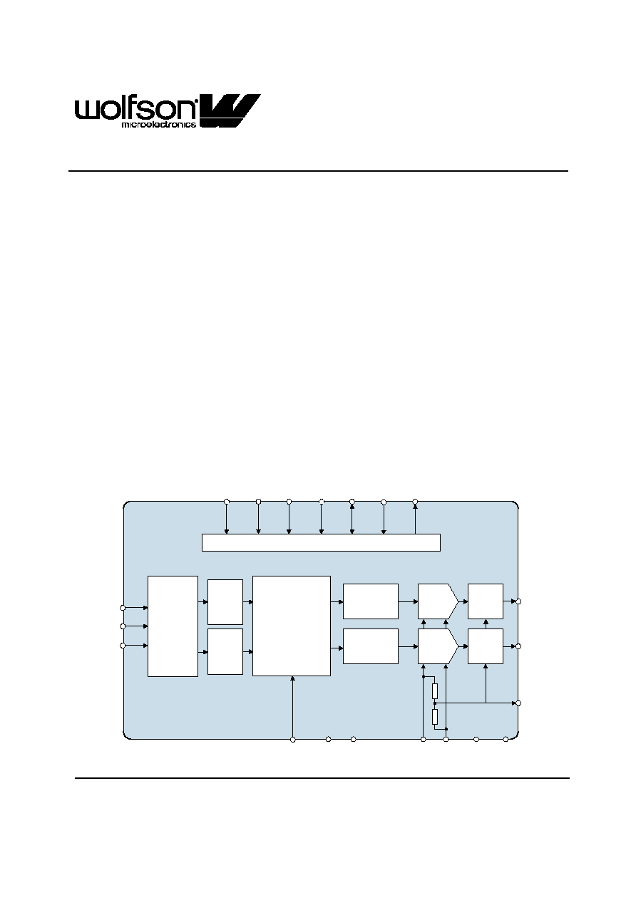
BLOCK DIAGRAM
BCKIN
SERIAL
INTERFACE
MUTE/
ATTEN
CONTROL INTERFACE
VOUTL
VOUTR
SIGMA
DELTA
MODULATOR
LRCIN
DIN
MUTE/
ATTEN
SIGMA
DELTA
MODULATOR
DIGITAL FILTERS
XTI
DVDD
AVDD
AGND
DGND
MUTEB
MDDM0
MCDM1
MLIIS
MODE
CSBIWO
ZERO
LOW
PASS
FILTER
LOW
PASS
FILTER
VMID
RIGHT
DAC
LEFT
DAC
VREFN
VREFP
WM8706
w

WM8706
Production Data
w
PD Rev 3.0 November 2002
2
PIN CONFIGURATION
ORDERING INFORMATION
DEVICE
TEMP. RANGE
PACKAGE
WM8706EDS
-25 to +85
o
C
28-pin SSOP
WM8706EDS/R
-25 to +85
o
C
28-pin SSOP
(tape and reel)
1
AGND
2
AVDD
3
NC
4
VOUTL
5
VMID
6
VREFN
7
VREFP
8
MCDM1
9
ZERO
10
NC
CSBIWO
MODE
MDDM0
MUTEB
15
DIN
MLIIS
DGND
NC
NC
XTI
BCKIN
LRCIN
NC
NC
DVDD
NC
NC
VOUTR
11
12
13
14
16
17
18
19
20
21
22
23
24
25
28
27
26
Note:
Reel quantity = 2,000

WM8706
Production Data
w
PD Rev 3.0 November 2002
3
PIN DESCRIPTION
PIN
NAME
TYPE
DESCRIPTION
1
LRCIN
Digital Input
DAC Sample Rate Clock Input
2
DIN
Digital Input
Serial Audio Data Input
3
BCKIN
Digital Input
Audio Data Bit Clock Input.
4
NC
No internal connection
5
XTI
Analogue Input
Master Clock Input
6
NC
No Internal Connection
7
DGND
Supply
Digital Ground Supply
8
DVDD
Supply
Digital Positive Supply
9
NC
No Internal Connection
10
NC
No Internal Connection
11
NC
No Internal Connection
12
NC
No Internal Connection
13
VOUTR
Analogue Output
Right Channel DAC Output
14
AGND
Supply
Analogue Ground Supply
15
AVDD
Supply
Analogue Positive Supply
16
VOUTL
Analogue Output
Left Channel DAC Output
17
NC
No Internal Connection
18
VMID
Analogue Output
Mid Rail Decoupling Point
19
VREFN
Supply
DAC Negative Reference � normally AGND, must not be below AGND
20
VREFP
Supply
DAC Positive Reference � normally AVDD, must not be above AVDD
21
ZERO
Digital Output
Infinite Zero Detect Flag
22
NC
No Internal Connection
23
CSBIWO
Digital Input
Software Mode: 3-Wire Serial Control Chip Select
Hardware Mode: Input Word Length, Pull Up
24
MODE
Digital Input
Control Mode Selection (Low = Hardware, High= Software), Pull Down
25
MUTEB
Digital Bi-directional
Mute Control (L = Mute on, H = Mute off, Z = Automute Enabled), Pull
Up
26
MDDM0
Digital Bi-directional
Software Mode: 3-Wire Serial Control Data Input:
Hardware Mode: De-Emphasis
27
MCDM1
Digital Input
Software Mode: 3-Wire Serial Control Clock Input
Hardware Mode: De-Emphasis, Pull Down
28
MLIIS
Digital Input
Software Mode 3-Wire Serial Control Load Input
Hardware Mode: Input Data Format Selection, Pull Up
Note:
Digital input pins have Schmitt trigger input buffers.

WM8706
Production Data
w
PD Rev 3.0 November 2002
4
ABSOLUTE MAXIMUM RATINGS
Absolute Maximum Ratings are stress ratings only. Permanent damage to the device may be caused by continuously operating at
or beyond these limits. Device functional operating limits and guaranteed performance specifications are given under Electrical
Characteristics at the test conditions specified.
ESD Sensitive Device. This device is manufactured on a CMOS process. It is therefore generically susceptible
to damage from excessive static voltages. Proper ESD precautions must be taken during handling and storage
of this device.
The WM8706 has been classified as MSL1, which has an unlimited floor life at <30
o
C / 85% Relative Humidity and therefore will
not be supplied in moisture barrier bags.
CONDITION
MIN
MAX
Digital supply voltage
-0.3V
+7V
Analogue supply voltage
-0.3V
+7V
Voltage range digital inputs
DGND -0.3V
DVDD +0.3V
Voltage range analogue inputs
AGND -0.3V
AVDD +0.3V
Master Clock Frequency (XTI)
50MHz
Operating temperature range, T
A
-25
�
C
+85
�
C
Storage temperature
-65
�
C
+150
�
C
Package body temperature (soldering 10 seconds)
+260
�
C
Package body temperature (soldering 2 minutes)
+183
�
C
Note:
Analogue and digital grounds must always be within 0.3V of each other.

WM8706
Production Data
w
PD Rev 3.0 November 2002
5
DC ELECTRICAL CHARACTERISTICS
PARAMETER
SYMBOL
TEST CONDITIONS
MIN
TYP
MAX
UNIT
Digital supply range
DVDD
3.0
5.5
V
Analogue supply range
AVDD
3.0
5.5
V
Ground
AGND, DGND
0
V
Difference DGND to AGND
-0.3
0
+0.3
V
Analogue supply current
AVDD = 5V
19
mA
Digital supply current
DVDD = 5V
8
mA
Analogue supply current
AVDD = 3.3V
18
mA
Digital supply current
DVDD = 3.3V
4
mA
ELECTRICAL CHARACTERISTICS
Test Conditions
AVDD, DVDD = 5V, AGND, DGND = 0V, T
A
= +25
o
C, fs = 48kHz, XTI = 256fs unless otherwise stated.
PARAMETER
SYMBOL
TEST CONDITIONS
MIN
TYP
MAX
UNIT
Digital Logic Levels (TTL Levels)
Input LOW level
V
IL
0.8
V
Input HIGH level
V
IH
2.0
V
Output LOW
V
OL
I
OL
= 1mA
AGND + 0.3V
V
Output HIGH
V
OH
I
OH
= 1mA
AVDD - 0.3V
V
Analogue Reference Levels
Reference voltage
VMID
(VREFP -
VREFN)/2 -
50mV
(VREFP -
VREFN)/2
(VREFP -
VREFN)2 +
50mV
V
Potential divider resistance
R
VMID
12k
ohms
DAC Output (Load = 10K ohms. 50pF)
0dBFs Full scale output voltage
At DAC outputs
1.1 x
AVDD/5
Vrms
SNR (Note 1,2,3)
A-weighted,
@ fs = 48kHz
100
106
dB
SNR (Note 1,2,3)
A-weighted
@ fs = 96kHz
106
dB
SNR (Note 1,2,3)
A-weighted
@ fs = 192kHz
106
dB
SNR (Note 1,2,3)
A-weighted,
@ fs = 48kHz
AVDD, DVDD = 3.3V
102
dB
SNR (Note 1,2,3)
A-weighted
@ fs = 96kHz
AVDD, DVDD = 3.3V
102
dB
SNR (Note 1,2,3)
Non `A' weigh ted @ fs
= 48kHz
103
dB
THD (Note 1,2,3)
1kHz, 0dBfs
-97
dB
THD+N (Dynamic range, Note 2)
1kHz, -60dBfs
100
106
dB
DAC channel separation
100
dB
WM8706
Production Data
w
PD Rev 3.0 November 2002
6
Test Conditions
AVDD, DVDD = 5V, AGND, DGND = 0V, T
A
= +25
o
C, fs = 48kHz, XTI = 256fs unless otherwise stated.
PARAMETER
SYMBOL
TEST CONDITIONS
MIN
TYP
MAX
UNIT
Analogue Output Levels
Load = 10k ohms,
0dBFS
1.1
V
RMS
Output level
Load = 10k ohms,
0dBFS,
(AVDD = 3.3V)
0.726
V
RMS
Gain mismatch
channel-to-channel
�1
%FSR
To midrail or a.c.
coupled
1
koh ms
Minimum resistance load
To midrail or a.c.
coupled
(AVDD = 3.3V)
600
ohms
Maximum capacitance load
5V or 3.3V
100
pF
Output d.c. level
(VREFP -
VREFN)/2
V
Power OnReset (POR)
POR threshold
2.4
V
Notes:
1.
Ratio of output level with 1kHz full scale input, to the output level with all zeros into the digital input, measured `A' weighted
over a 20Hz to 20kHz bandwidth.
2.
All performance measurements done with 20kHz low pass filter, and where noted an A-weight filter. Failure to use such a
filter will result in higher THD+N and lower SNR and Dynamic Range readings than are found in the Electrical
Characteristics. The low pass filter removes out of band noise; although it is not audible it may affect dynamic specification
values.
3.
VMID decoupled with10uF and 0.1uF capacitors (smaller values may result in reduced performance).
TERMINOLOGY
1.
Signal-to-noise ratio (dB) - SNR is a measure of the difference in level between the full scale output and the output with no
signal applied. (No Auto-zero or Automute function is employed in achieving these results).
2.
Dynamic range (dB) - DNR is a measure of the difference between the highest and lowest portions of a signal. Normally a
THD+N measurement at 60dB below full scale. The measured signal is then corrected by adding the 60dB to it. (e.g.
THD+N @ -60dB= -32dB, DR= 92dB).
3.
THD+N (dB) - THD+N is a ratio, of the rms values, of (Noise + Distortion)/Signal.
4.
Stop band attenuation (dB) - Is the degree to which the frequency spectrum is attenuated (outside audio band).
5.
Channel Separation (dB) - Also known as Cross-Talk. This is a measure of the amount one channel is isolated from the
other. Normally measured by sending a full scale signal down one channel and measuring the other.

WM8706
Production Data
w
PD Rev 3.0 November 2002
7
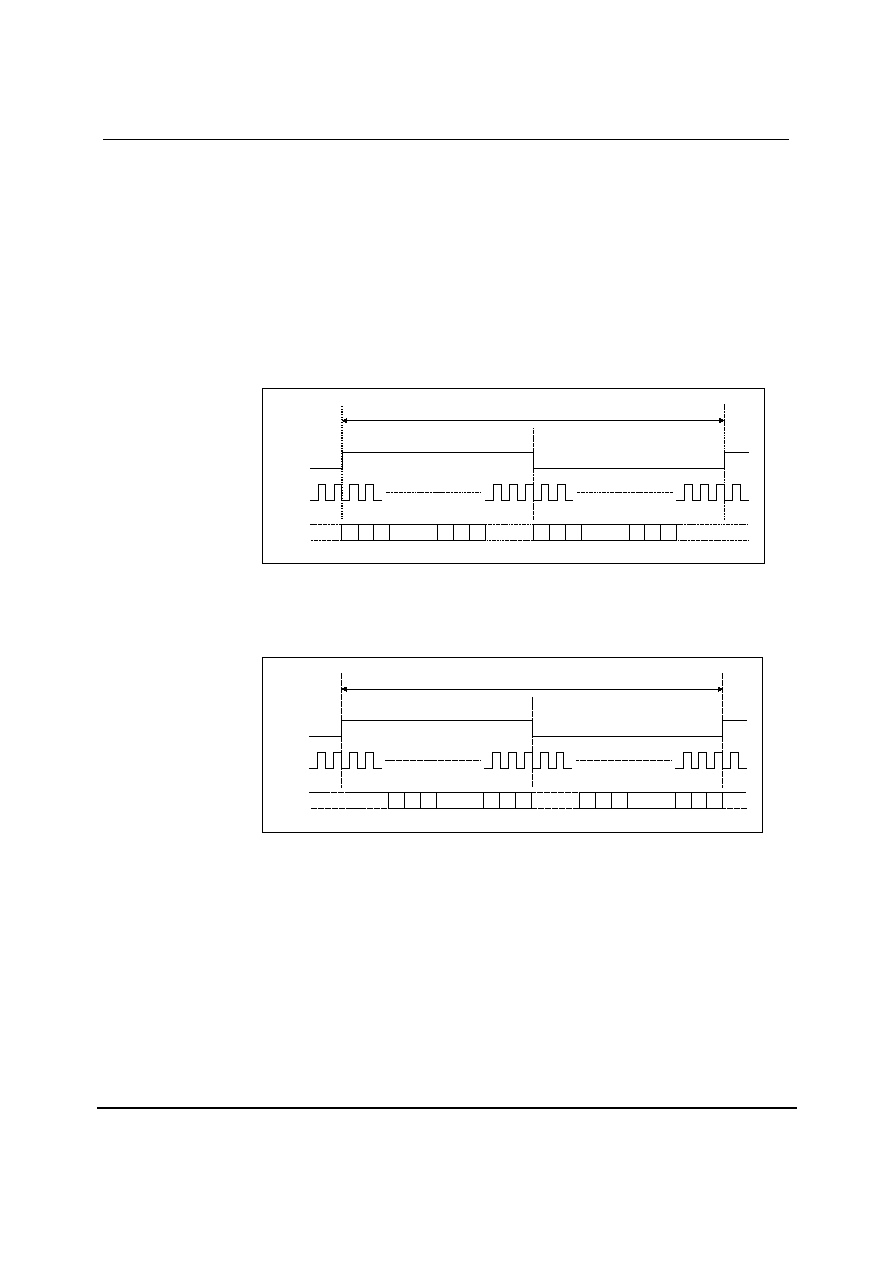
MASTER CLOCK TIMING
XTI
t
XTIL
t
XTIH
t
XTIY
Figure 1 Master Clock Timing Requirements
Test Conditions
AVDD, DVDD = 5V, AGND, DGND = 0V, T
A
= +25
o
C, fs = 48kHz, XTI = 256fs unless otherwise stated.
PARAMETER
SYMBOL
TEST CONDITIONS
MIN
TYP
MAX
UNIT
Master Clock Timing Information
XTI Master clock pulse widthhigh
t
XTIH
13
ns
XTI Master clock pulse widthlow
t
XTIL
13
ns
XTI Master clock cycle time
t
XTIY
26
ns
XTI Duty cycle
40:60
60:40
DIGITAL AUDIO INTERFACE
BCKIN
LRCIN
t
BCH
t
BCL
t
BCY
DIN
t
LRSU
t
DS
t
LRH
t
DH
Figure 2 Digital Audio Data Timing
Test Conditions
AVDD, DVDD = 5V, AGND, DGND = 0V, T
A
= +25
o
C, fs = 48kHz, XTI = 256fs unless otherwise stated.
PARAMETER
SYMBOL
TEST CONDITIONS
MIN
TYP
MAX
UNIT
Audio Data Input Timing Information
BCKIN cycle time
t
BCY
40
ns
BCKIN pulse widthhigh
t
BCH
16
ns
BCKIN pulse widthlow
t
BCL
16
ns
LRCIN set-up time to
BCKIN rising edge
t
LRSU
8
ns
LRCIN hold time from
BCKIN rising edge
t
LRH
8
ns
DIN set-up time to BCKIN
rising edge
t
DS
8
ns
DIN h old time from BCKIN
rising edge
t
DH
8
ns

WM8706
Production Data
w
PD Rev 3.0 November 2002
8
MPU INTERFACE TIMING
MLIIS
MCDM1
MDDM0
t
CSL
t
DHO
t
DSU
t
CSH
t
SCY
t
SCH
t
SCL
t
SCS
LSB
t
CSS
CSBIWO
t
CSSH
t
CSSU
Figure 3 Program Register Input Timing - 3-Wire Serial Control Mode
Test Conditions
AVDD, DVDD = 5V, AGND, DGND = 0V, T
A
= +25
o
C, fs = 48kHz, XTI = 256fs unless otherwise stated.
PARAMETER
SYMBOL
TEST CONDITIONS
MIN
TYP
MAX
UNIT
Program Register Input Information
MCDM1 rising edge to MLIIS
rising edge
t
SCS
40
ns
MCDM1 pulse cycle time
t
SCY
80
ns
MCDM1 pulse widthlow
t
SCL
20
ns
MCDM1 pulse widthhigh
t
SCH
20
ns
MDDM0 to MCDM1 set-up time
t
DSU
20
ns
MCDM1 to MDDM0 h old time
t
DHO
20
ns
MLIIS pulse widthlow
t
CSL
20
ns
MLIIS pulse widthhigh
t
CSH
20
ns
MLIIS rising to SCLK rising
t
CSS
20
ns
CSBIWO to MLIIS set-up time
t
CSSU
20
Ns
MLIIS to CSBIWO hold time
t
CSSH
20
ns

WM8706
Production Data
w
PD Rev 3.0 November 2002
9
DEVICE DESCRIPTION
INTRODUCTION
The WM8706 is a high performance DAC designed for digital consumer audio applications. Its
range of features make it ideally suited for use in DVD players, AV receivers and other high end
consumer audio equipment.
The WM8706 is a complete 2-channel stereo audio digital-to-analogue converter, including
digital interpolation filter, multi-bit sigma delta with dither, and switched capacitor multi-bit
stereo DAC and output smoothing filters. The WM8706 includes an on-board digital volume
control, configurable digital audio interface and a 3 wire MPU control interface. It is fully
compatible and an ideal partner for a range of industry standard microprocessors, controllers
and DSPs.
Control of internal functionality of the device is by either hardware control (pin programmed) or
software control (3-wire serial control interface). The MODE pin selects between hardware and
software control. The software control interface may be asynchronous to the audio data
interface. Control data will be re-synchronised to the audio processing internally.
Operation using master clocks of 256fs, 384fs, 512fs or 768fs is provided, selection between
clock rates being automatically controlled in hardware mode, or serial controlled when in
software mode. Sample rates (fs) from less than 8ks/s to 96ks/s are allowed, provided the
appropriate master clock is input. Support is also provided for up to 192ks/s using a master
clock of 128fs or 192fs.
The audio data interface supports right, left and I
2
S (Philips left justified, one bit delayed)
interface formats along with a highly flexible DSP serial port interface. When in hardware mode,
the three serial interface pins become control pins to allow selection of input data format type
(I
2
S or right justified), input word length (16, 20, or 24-bit) and de-emphasis functions.
The device is packaged in a small 28-pin SSOP and is a pin-compatible alternative to the
WM8716.
CLOCKING SCHEMES
In a typical digital audio system there is only one central clock source producing a reference
clock to which all audio data processing is synchronised. This clock is often referred to as the
audio system's Master Clock. The external master system clock can be applied directly through
the XTI input pin with no software configuration necessary for sample rate selection.
Note that on the WM8706, XTI is used to derive clocks for the DAC path. The DAC path
consists of DAC sampling clock, DAC digital filter clock and DAC digital audio interface timing.
In a system where there are a number of possible sources for the reference clock it is
recommended that the clock source with the lowest jitter be used to optimise the performance
of the DAC.
DIGITAL AUDIO INTERFACE
Audio data is applied to the internal DAC filters via the Digital Audio Interface. 5 popular
interface formats are supported:
�
Left Justified mode
�
Right Justified mode
�
I
2
S mode
�
DSP Early mode
�
DSP Late mode
All 5 formats send the MSB first and support word lengths of 16, 20, 24 and 32 bits. The
exception is that 32 bit data is not supported in right justified mode. DIN and LRCIN are
sampled on the rising, or falling edge of BCKIN depending on the format selected.
In left justified, right justified and I
2
S modes, the digital audio interface receives data on the DIN
input. Audio Data is time multiplexed with LRCIN indicating whether the left or right channel is
present. LRCIN is also used as a timing reference to indicate the beginning or end of the data
words.
WM8706
Production Data
w
PD Rev 3.0 November 2002
10
In left justified, right justified and I
2
S modes, the minimum number of BCKINs per LRCIN period
is 2 times the selected word length. LRCIN must be high for a minimum of word length BCKINs
and low for a minimum of word lengthBCKINs. Any mark to space ratio on LRCIN is
acceptable provided the above requirements are met. The WM8706 will automatically detect
when data with a LRCIN period of exactly 32 is sent, and select 16 bit mode - overriding any
previously programmed word length. Word length will revert to the previously programmed
value when a LRCIN period other than 32 is detected. (see Figure 4, Figure 5 and Figure 6).
In DSP early or DSP late mode, the data is time multiplexed onto DIN. LRCIN is used as a
frame sync signal to identify the MSB of the first word. The minimum number of BCKINs per
LRCIN period is 2 times the selected word length. Any mark to space ratio is acceptable on
LRCIN provided the rising edge is correctly positioned (see Figure 7 and Figure 8).
LEFT JUSTIFIED MODE
In left justified mode, the MSB is sampled on the first rising edge of BCKIN following a LRCIN
transition. LRCIN is high during the left samples and low during the right samples.
LEFT CHANNEL
RIGHT CHANNEL
LRCIN
BCKIN
DIN
1/fs
n
3
2
1
n-2 n-1
LSB
MSB
n
3
2
1
n-2 n-1
LSB
MSB
Figure 4 Left Justified Mode Timing Diagram
RIGHT JUSTIFIED MODE
In right justified mode, the LSB is sampled on the rising edge of BCKIN preceding a LRCIN
transition. LRCIN is high during the left samples and low during the right samples.
LEFT CHANNEL
RIGHT CHANNEL
LRCIN
BCKIN
DIN
1/fs
n
3
2
1
n-2 n-1
LSB
MSB
n
3
2
1
n-2 n-1
LSB
MSB
Figure 5 Right Justified Mode Timing Diagram

WM8706
Production Data
w
PD Rev 3.0 November 2002
11
I
2
S MODE
In I
2
S mode, the MSB is sampled on the second rising edge of BCKIN following a LRCIN
transition. LRCIN is low during the left samples and high during the right samples.
LEFT CHANNEL
RIGHT CHANNEL
LRCIN
BCKIN
DIN
1/fs
n
3
2
1
n-2 n-1
LSB
MSB
n
3
2
1
n-2 n-1
LSB
MSB
1 BCKIN
1 BCKIN
Figure 6 I
2
S Mode Timing Diagram
DSP EARLY MODE
In DSP early mode, the first bit is sampled on the BCKIN rising edge following the one which
detects a low to high transition on LRCIN. No BCKIN edges are allowed between the data
words. The word order is DIN left, DIN right.
LRCIN
BCKIN
DIN
Input Word Length(IWO)
1/fs
LEFT CHANNEL
n
2
1
n-1
LSB
MSB
n
2
1
n-1
RIGHT CHANNEL
NO VALID DATA
1 BCKIN
1 BCKIN
Figure 7 DSP Early Mode Timing Diagram
DSP LATE MODE
In DSP late mode, the first bit is sampled on the BCKIN rising edge which detects a low to high
transition on LRCIN. No BCKIN edges are allowed between the data words. The word order is
DIN left, DIN right.
LRCIN
BCKIN
DIN
Input Word Length(IWO)
1/fs
LEFT CHANNEL
n
2
1
n-1
LSB
MSB
n
2
1
n-1
RIGHT CHANNEL
NO VALID DATA
1
Figure 8 DSP Late Mode Timing Diagram

WM8706
Production Data
w
PD Rev 3.0 November 2002
12
AUDIO DATA SAMPLING RATES
The master clock for WM8706 supports audio sampling rates from 128fs to 768fs, where fs is
the audio sampling frequency (LRCIN) typically 32kHz, 44.1kHz, 48kHz, 96kHz or 192kHz. The
master clock is used to operate the digital filters and the noise shaping circuits.
The WM8706 has a master clock detection circuit that automatically determines the relation
between the master clock frequency and the sampling rate (to within +/- 32 master clocks). If
there is a greater than 8 clocks error, the interface shuts down the DAC and mutes the output.
The master clock should be synchronised with LRCIN, although the WM8706 is tolerant of
phase differences or jitter on this clock.
MASTER CLOCK FREQUENCY (MHZ) (XTI)
SAMPLING
RATE
(LRCIN)
128fs
192fs
256fs
384fs
512fs
768fs
32kHz
4.096
6.144
8.192
12.288
16.384
24.576
44.1kHz
5.6448
8.467
11.2896
16.9340
22.5792
33.8688
48kHz
6.114
9.216
12.288
18.432
24.576
36.864
96kHz
12.288
18.432
24.576
36.864
Unavailable
Unavailable
192kHz
24.576
36.864
Unavailable
Unavailable
Unavailable
Unavailable
Table 1 Typical Relationships Between System Frequency and Sampling Rates.
HARDWARE CONTROL MODES
When the MODE pin is held low, the following hardware modes of operation are available.
MUTE AND AUTOMUTE OPERATION
In bothhardware and software modes, pin 25 (MUTEB) controls selection of MUTE directly, and
can be used to enable and disable the automute function, or as an output of the automuted signal.
MUTEB PIN
DESCRIPTION
0
Mute DAC channels
1
Normal Operation
Floating
Enable IZD, MUTEB becomes an output to indicate when IZD occurs.
Table 2 Mute and Automute Control
Figure 9 shows the application and release of MUTE whilst a full amplitude sinusoid is being
played at 48kHz sampling rate. When MUTE (lower trace) is asserted, the output (upper trace)
begins to decay exponentially from the DC level of the last input sample. The output will decay
towards V
MID
witha time constant of approximately 64 input samples. Wh
en MUTE is de-
asserted, the output will restart almost immediately from the current input sample.

WM8706
Production Data
w
PD Rev 3.0 November 2002
13
-2.5
-2
-1.5
-1
-0.5
0
0.5
1
1.5
0
0.001
0.002
0.003
0.004
0.005
0.006
Time(s)
Figure 9 Applicationand Release of Soft Mute
The MUTEB pin is an input to select mute or not mute. MUTEB is active low; taking the pin low
causes the filters to soft mute, ramping down the audio signal over a few milliseconds. Taking
MUTEB high again allows data into the filter.
The automute function detects a series of zero value audio samples of 1024 samples long
being applied to bothch
annels. After suchan event, a latchis set wh
ose output
(AUTOMUTED) is wire OR'ed through a 10kohm resistor to the MUTEB pin. Thus if the
MUTEB pin is not being driven, the automute function will assert mute.
If MUTEB is tied high, AUTOMUTE is overridden and will not mute unless the IZD register bit is
set. If MUTEB is driven from a bi-directional source, then both MUTE and automute functions
are available. If MUTEB is not driven, AUTOMUTED appears as a weak output (10k source
impedance) so can be used to drive external mute circuits. Automute will be removed as soon
as any channel receives a non-zero input.
A diagram showing how the various Mute modes interact is shown below in Figure 10.
IZD (Register Bit)
AUTOMUTED
(Internal Signal)
10k
MUT (Register Bit)
SOFTMUTE
(Internal
Signal)
MUTEB
PIN
Figure 10 SelectionLogic for MUTE Modes
WM8706
Production Data
w
PD Rev 3.0 November 2002
14
INPUT FORMAT SELECTION
In hardware mode, MLIIS (pin 28) and CSBIWO (pin 23) become input controls for selection of
input data format type and input data word length.
MLIIS
CSBIWO
INPUT DATA MODE
0
0
24-bit right justified**
0
1
20-bit right justified
1
0
16-bit I
2
S
1
1
24-bit I
2
S
Table 3 Input Format Selection
Note:
In 24 bit I
2
S mode, any width of 24 bits or less is supported provided that LRCIN is high for a
minimum of 24 BCKINs and low for a minimum of 24 BCKINs.
** This mode differs from the WM8716 which does 16-bit right justified in this mode.
The
previous mode is still available by using exactly 32 BCKIN per LRCIN cycle, 16 for left and
right. This mode is automatically detected within the hardware and overrides the data width
specified but not the format.
DE-EMPHASIS CONTROL
In hardware mode, MCDM1 (pin 27) and MDDM0 (pin 26) become input controls for selection
of de-emphasis filtering to be applied.
MCDM1
MDDM0
DE-EMPHASIS**
0
0
Off
0
1
48kHz
1
0
44.1kHz
1
1
32kHz
Table 4 De-emphasis Control
Note:
** The actual de-emphasis within the WM8706 is the same for all data rates. This differs from
WM8716 which has a different response for each sample rate.
SOFTWARE CONTROL INTERFACE
SELECTION OF CONTROL MODE
The WM8706 may be programmed to operate in hardware or software control modes. This is
achieved by setting the state of the MODE pin.
MODE
INTERFACE FORMAT
0
Hardware Control Mode
1
Software Control Mode
Table 5 Control Interface Mode Selection

WM8706
Production Data
w
PD Rev 3.0 November 2002
15
3-WIRE (SPI COMPATIBLE) SERIAL CONTROL MODE
The WM8706 can be controlled using a 3-wire serial interface. MDDM0 is used for the program
data, MCDM1 is used to clock in the program data and MLIIS is used to latch in the program
data. The 3-wire interface protocol is shown in Figure 11.
MLIIS
MCDM1
MDDM0
B15
B6
B7
B8
B9
B10
B11
B12
B13
B14
B1
B2
B3
B4
B5
B0
Figure 11 3-Wire Serial Interface
Notes:
1.
B[15:9] are Control Address Bits
2.
B[8:0] are Control Data Bits
REGISTER MAP
WM8706 uses a total of 4 programme registers, which are 16-bits long. These registers are all
loaded through input pin MDDM0. After the 16 data bits are clocked in, MLIIS is used to latch in
the data to the appropriate register. Table 6 shows the complete mapping of the
4 registers.
B15
B14
B13
B12
B11
B10
B9
B8
B7
B6
B5
B4
B3
B2
B1
B0
M0
0
0
0
0
0
0
0
UPDATEL
LAT7
LAT6
LAT5
LAT4
LAT3
LAT2
LAT1
LAT0
M1
0
0
0
0
0
0
1
UPDATER
RAT7
RAT6
RAT5
RAT4
RAT3
RAT2
RAT1
RAT0
M2
0
0
0
0
0
1
0
0
0
0
IW2
IW1
IW0
PWRDN DEEMPH
MUT
M3
0
0
0
0
0
1
1
IZD
SF1
SF0
BCP
REV
0
ATC
LRP
I
2
S
ADDRESS
DATA
Table 6 Mapping of Program Registers

WM8706
Production Data
w
PD Rev 3.0 November 2002
16
REGISTER
ADDRESS
A2, A1, A0
BITS
LABEL
DEFAULT
DESCRIPTION
[7:0]
LAT[7:0]
11111111 (0dB)
Attenuation data for left channel in 0.5dB steps.
000
A2, A1, A0
DACL
Attenuation
8
UPDATEL
0
Attenuation data load control for left channel.
0: Store DACL in intermediate latch(no change to output)
1: Store DACL and update attenuation on all channels.
[7:0]
RAT[7:0]
11111111 (0dB)
Attenuation data for right channel in 0.5dB steps.
001
DACR
Attenuation
8
UPDATER
0
Attenuation data load control for right channel.
0: Store DACR in intermediate latch(no change to output)
1: Store DACR and update attenuation on all channels.
0
MUT
0
Left and right DACs soft mute control.
0: No mute
1: Mute
1
DEEMPH
0
De-emphasis control.
0: De-emphasis off
1: De-emphasis on
2
PWDN
0
Left and Right DACs Power-down Control
0: All DACs running, output is active
1: All DACs in power saving mode, output muted
010
DAC Control
[5:3]
IW[2:0]
000
Audio data format select.
0
I
2
S
0
Audio data format select.
1
LRP
0
Polarity select for LRCIN/DSP mode select.
0: normal LRCIN polarity/DSP late mode
1: inverted LRCIN polarity/DSP early mode
2
ATC
0
Attenuator Control.
0: All DACs use attenuations as programmed.
1: Right channel DACs use corresponding left DAC
attenuations
4
REV
0
Output phase reverse.
5
BCP
0
BCKIN Polarity
0 : normal BCKIN polarity
1: inverted BCKIN polarity
[7:6]
SF[1:0]
00
De-Emphasis sample rate select.
011
Interface
Control
8
IZD
0
Infinite zero detection circuit control and automute control
0: Infinite zero detect disabled
1: Infinite zero detect enabled
Table 7 Register Bit Descriptions

WM8706
Production Data
w
PD Rev 3.0 November 2002
17
ATTENUATION CONTROL
Each DAC channel can be attenuated digitally before being applied to the digital filter. Attenuation is 0dB by default but can be
set between 0 and 127.5dB in 0.5dB steps using the 8 Attenuation control bits. All attenuation registers are double latched
allowing new values to be pre-latched to both channels before being updated synchronously. Setting the UPDATE bit on any
attenuation write will cause all pre-latched values to be immediately applied to the DAC channels.
REGISTER
ADDRESS
A2, A1, A0
BIT
LABEL
DEFAULT
DESCRIPTION
7:0
LAT[7:0]
11111111
(0dB)
Attenuation data for Left channel DACL in 0.5dB steps.
000
DACL
Attenuation
8
UPDATEL
0
Controls simultaneous update of all Attenuation Latches
0: Store DACL in intermediate latch(no change to output)
1: Store DACL and update attenuation on all channels.
7:0
RAT[7:0]
11111111
(0dB)
Attenuation data for Right channel DACR in 0.5dB steps.
001
DACR
Attenuation
8
UPDATER
0
Controls simultaneous update of all Attenuation Latches
0: Store DACR in intermediate latch(no change to output)
1: Store DACR and update attenuation on all channels.
Table 8 Attenuation Register Map
Note:
1.
The UPDATE bit is not latched. If UPDATE=0, the Attenuation value will be written to the pre-latch but not applied to the
relevant DAC. If UPDATE=1, all pre-latched values will be applied from the next input sample.
2.
Care should be used in reducing the attenuation as rapid large volume changes can introduce zipper noise.
DAC OUTPUT ATTENUATION
Registers LAT and RAT control the left and right channel attenuation. Table 9 shows how the
attenuation levels are selected from the 8-bit words.
XAT[7:0]
ATTENUATION LEVEL
00(hex)
dB (mute)
01(hex)
127.5dB
:
:
:
:
:
:
FE(hex)
0.5dB
FF(hex)
0dB
Table 9 Attenuation Control Levels
MUTE MODES
Setting the MUT register bit will apply a 'soft' mute to the input of the digital filters:
REGISTER ADDRESS
BIT
LABEL
DEFAULT
DESCRIPTION
010
DAC Control
0
MUT
0
Soft Mute select
0 : Normal Operation
1: Soft mute all channels
Table 10 Mute Control
DE-EMPHASIS MODE
Setting the DEEMPH register bit puts the all the digital filters into de-emphasis mode:
REGISTER ADDRESS
BIT
LABEL
DEFAULT
DESCRIPTION
010
DAC Control
1
DEEMPH
0
De-emphasis mode select:
0 : De-emphasis Off
1: De-emphasis On
Table 11 De-emphasis Control

WM8706
Production Data
w
PD Rev 3.0 November 2002
18
POWERDOWN MODE
Setting the PWDN register bit immediately connects all outputs to V
MID
and selects a low power
mode. All trace of the previous input samples is removed, and all register settings are cleared.
When PWDN is cleared again the first 16 input samples will be ignored as the FIR will repeat
it's power-on initialisation sequence.
REGISTER ADDRESS
BIT
LABEL
DEFAULT
DESCRIPTION
010
DAC Control
2
PWDN
0
Power Down Mode Select:
0 : Normal Mode
1: Power Down Mode
Table 12 PowerdownControl
DIGITAL AUDIO INTERFACE CONTROL REGISTERS
The WM8706 has a fully featured digital audio interface that is a superset of that contained in
the WM8716. Interface format is selected via the IW[2:0] register bits in register M2 and the I
2
S
register bit in M3.
REGISTER ADDRESS
BIT
LABEL
DEFAULT
DESCRIPTION
010
DAC Control
5:3
IW[2:0]
000
Interface format Select
Table 13 Interface Format Controls
REGISTER ADDRESS
BIT
LABEL
DEFAULT
DESCRIPTION
011
Interface Control
0
I
2
S
0
Interface format Select
Table 14 Interface Format Control
IW2
I
2
S
IW1
IW0
AUDIO INTERFACE DESCRIPTION **
0
0
0
0
16 bit right justified mode
0
0
0
1
20 bit right justified mode
0
0
1
0
24 bit right justified mode
0
0
1
1
24 bit left justified mode
0
1
0
0
16 bit I
2
S mode
0
1
0
1
24 bit I
2
S mode
0
1
1
0
20 bit I
2
S mode
0
1
1
1
20 bit left justified (MSB first) mode
1
0
0
0
16 bit DSP mode
1
0
0
1
20 bit DSP mode
1
0
1
0
24 bit DSP mode
1
0
1
1
32 bit DSP mode
1
1
0
0
16 bit left justified mode
Table 15 Audio Data Input Format
Note:
** In all modes, the data is signed 2's complement. The digital filters always input 24-bit data. If
the DAC is programmed to receive 16 or 20 bit data, the WM8706 pads the unused LSBs with
zeros. If the DAC is programmed into 32 bit mode, the 4 LSBs are ignored.
SELECTION OF LRCIN POLARITY
In left justified, right justified or I
2
S modes, the LRP register bit controls the polarity of LRCIN. If
this bit is set high, the expected polarity of LRCIN will be the opposite of that shown in Figure 4,
Figure 5 and Figure 6. Note that if this feature is used as a means of swapping the left and
right channels, a 1 sample phase difference will be introduced.
REGISTER ADDRESS
BIT
LABEL
DEFAULT
DESCRIPTION
011
Interface Control
1
LRP
0
LRCIN Polarity (normal)
0 : normal LRCIN polarity
1: inverted LRCIN polarity
Table 16 LRCIN Polarity Control

WM8706
Production Data
w
PD Rev 3.0 November 2002
19
In DSP modes, the LRCIN register bit is used to select between early and late modes:
REGISTER ADDRESS
BIT
LABEL
DEFAULT
DESCRIPTION
011
Interface Control
1
LRP
0
DSP Format (DSP modes)
0 : Early DSP mode
1: Late DSP mode
Table 17 DSP Format Control
In DSP early mode, the first bit is sampled on the BCKIN rising edge following the one that
detects a low to high transition on LRCIN. In DSP late mode, the first bit is sampled on the
BCKIN edge, which detects a low to high transition on LRCIN. No BCKIN rising edges are
allowed between the data words. The word order is DIN left, DIN right.
ATTENUATOR CONTROL MODE
Setting the ATC register bit causes the left channel attenuation settings to be applied to both
left and right channel DACs from the next audio input sample. No update to the attenuation
registers is required for ATC to take effect.
REGISTER ADDRESS
BIT
LABEL
DEFAULT
DESCRIPTION
011
Interface Control
2
ATC
0
Attenuate Control Mode:
0 : Right channels use Right
attenuation
1:
Right Channels use Left
Attenuation
Table 18 Attenuation Control Select
OUTPUT PHASE REVERSAL
The REV register bit controls the phase of the output signal. Setting the REV bit causes the
phase of the output signal to be inverted.
REGISTER ADDRESS
BIT
LABEL
DEFAULT
DESCRIPTION
011
Interface Control
4
REV
0
Analogue Output Phase
0: Normal
1: Inverted
Table 19 Output Phase Control
BCKIN POLARITY
By default, LRCIN and DIN are sampled on the rising edge of BCKIN and should ideally change
on the falling edge. Data sources which change LRCIN and DIN on the rising edge of BCKIN
can be supported by setting the BCP register bit. Setting BCP to 1 inverts the polarity of BCKIN
to the inverse of that shown in Figure 4, Figure 5, Figure 6, Figure 7 and Figure 8.
REGISTER ADDRESS
BIT
LABEL
DEFAULT
DESCRIPTION
011
Interface Control
5
BCP
0
BCKIN Polarity
0 : normal BCKIN polarity
1: inverted BCKIN polarity
Table 20 BCKIN Polarity Control
DE-EMPHASIS SAMPLE RATE SELECTION
The SF[1:0] bits are used to select the de-emphasis rate.
REGISTER ADDRESS
BIT
LABEL
DEFAULT
DESCRIPTION **
0011
Interface Control
7:6
SF[1:0]
00
De-Emphasis Sample Rate Selection
00 : De-Emphasis Off
01: 48kHz
10: 44.1kHz
11: 32kHz
Table 21 De-emphasis Control
Note:
** There is only one internal de-emphasis mode optimised for 44.1kHz. This is in contrast to
WM8716 whichis individually optimised for eachsample rate.

WM8706
Production Data
w
PD Rev 3.0 November 2002
20
INFINITE ZERO DETECTION
Setting the IZD register bit determines whether the device is automuted when a sequence of
more than 1024 zeros is detected.
REGISTER ADDRESS
BIT
LABEL
DEFAULT
DESCRIPTION
011
Interface Control
8
IZD
0
Infinite zero detection circuit control
and automute control
0: Infinite zero detect disabled
1: Infinite zero detect enabled
Table 22 IZD Control
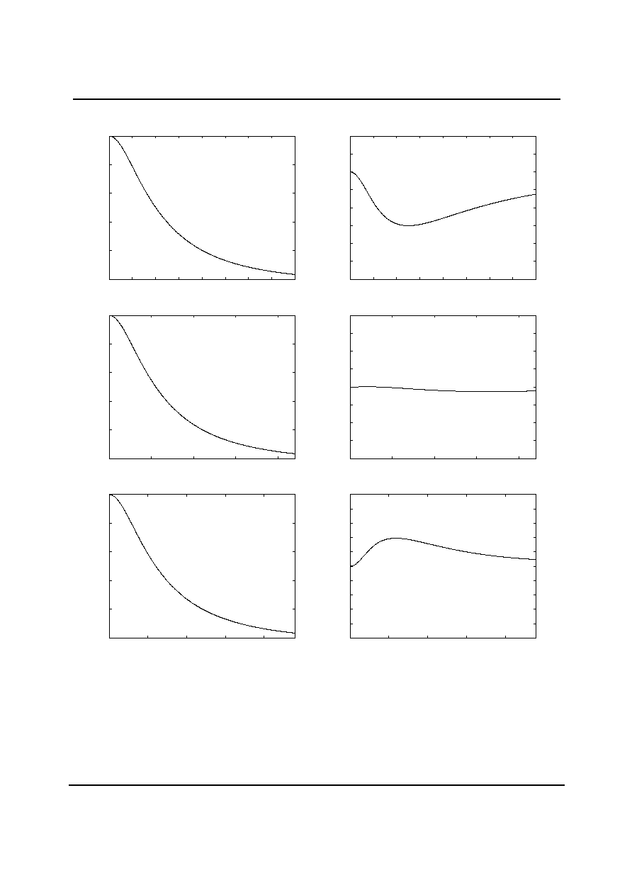
DIGITAL FILTER CHARACTERISTICS
PARAMETER
SYMBOL
TEST CONDITIONS
MIN
TYP
MAX
UNIT
Passband Edge
-3dB
0.487fs
Passband Ripple
f < 0.444fs
�
0.05
dB
Stopband Attenuation
f > 0.555fs
-60
dB
Table 23 Digital Filter Characteristics
DAC FILTER RESPONSES
-120
-100
-80
-60
-40
-20
0
0
0.5
1
1.5
2
2.5
3
Response (dB)
Frequency (Fs)
Figure 12 DAC Digital Filter Frequency Response
- 44.1, 48 and 96kHz
-0.2
-0.15
-0.1
-0.05
0
0.05
0.1
0.15
0.2
0
0.05
0.1
0.15
0.2
0.25
0.3
0.35
0.4
0.45
0.5
Response (dB)
Frequency (Fs)
Figure 13 DAC Digital Filter Ripple - 44.1, 48 and 96kHz
-80
-60
-40
-20
0
0
0.2
0.4
0.6
0.8
1
Response (dB)
Frequency (Fs)
Figure 14 DAC Digital Filter Frequency Response
- 192kHz
-1
-0.8
-0.6
-0.4
-0.2
0
0.2
0
0.05
0.1
0.15
0.2
0.25
0.3
0.35
0.4
0.45
0.5
Response (dB)
Frequency (Fs)
Figure 15 DAC Digital Filter Ripple - 192kHz
WM8706
Production Data
w
PD Rev 3.0 November 2002
21
DIGITAL DE-EMPHASIS CHARACTERISTICS
-10
-8
-6
-4
-2
0
0
2
4
6
8
10
12
14
16
Response (dB)
Frequency (kHz)
Figure 16 De-Emphasis Frequency Response (32kHz)
-3
-2.5
-2
-1.5
-1
-0.5
0
0.5
1
0
2
4
6
8
10
12
14
16
Response (dB)
Frequency (kHz)
Figure 17 De-Emphasis Error (32kHz)
-10
-8
-6
-4
-2
0
0
5
10
15
20
Response (dB)
Frequency (kHz)
Figure 18 De-Emphasis Frequency Response (44.1kHz)
-0.4
-0.3
-0.2
-0.1
0
0.1
0.2
0.3
0.4
0
5
10
15
20
Response (dB)
Frequency (kHz)
Figure 19 De-Emphasis Error (44.1kHz)
-10
-8
-6
-4
-2
0
0
5
10
15
20
Response (dB)
Frequency (kHz)
Figure 20 De-Emphasis Frequency Response (48kHz)
-1
-0.8
-0.6
-0.4
-0.2
0
0.2
0.4
0.6
0.8
1
0
5
10
15
20
Response (dB)
Frequency (kHz)
Figure 21 De-Emphasis Error (48kHz)

WM8706
Production Data
w
PD Rev 3.0 November 2002
22
RECOMMENDED EXTERNAL COMPONENTS
28
DVDD
DGND
MLIIS
AGND
AVDD
VMID
C
9
C
8
AGND
8
7
Software I/F or
Hardware Control
WM8706
Notes:
1. AGND and DGND should be connected as close to the WM8706 as possible.
2. C
2
, C
3
, C
4
and C
8
should be positioned as close to the WM8706 as possible.
3. Capacitor types should be carefully chosen. Capacitors with very low ESR are
recommended for optimum performance.
VREFP
VREFN
C
3
C
4
C
5
C
2
DVDD
C
1
27
MCDM1
26
MDDM0
VOUTR
16
C
6
VOUTL
C
7
AC-Coupled
VOUTR/L
to External LPF
24
MODE
25
MUTEB
13
AVDD
5
XTI
3
BCKIN
2
DIN
Audio Serial Data I/F
DGND
AGND
1
LRCIN
15
20
14
19
+
+
+
18
+
+
Software/hardware
control mode select
21
ZERO
23
CSBIWO
Figure 22 External Components Diagram
RECOMMENDED EXTERNAL COMPONENT VALUES
COMPONENT
REFERENCE
SUGGESTED
VALUE
DESCRIPTION
C1 and C5
10
�
F
De-coupling for DVDD and AVDD/VREFP
C2 to C4
0.1
�
F
De-coupling for DVDD and AVDD/VREFP
C6 and C7
10
�
F
Output AC coupling caps to remove midrail DC level from outputs.
C8
0.1
�
F
C9
10
�
F
Reference de-coupling capacitors for VMID pin.
Table 24 External Components Description

WM8706
Production Data
w
PD Rev 3.0 November 2002
23
RECOMMENDED ANALOGUE LOW PASS FILTER (OPTIONAL)
+
_
+
+VS
-VS
10uF
51
7.5K
680pF
1.8k
47k
4.7k
4.7k
1.0nF
Figure 23 Recommended Low Pass Filter (Optional)
WM8706
Production Data
w
PD Rev 3.0 November 2002
24
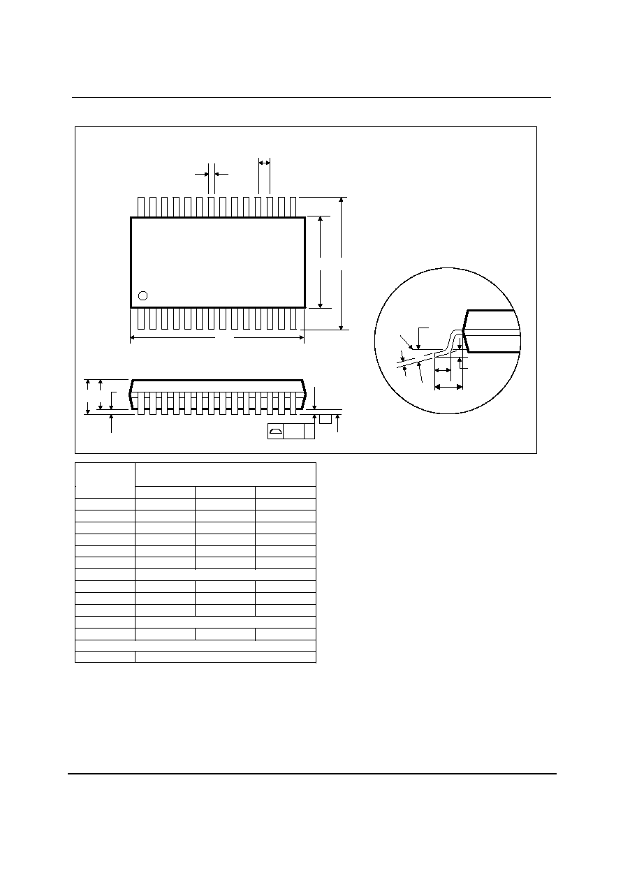
PACKAGE DIMENSIONS
NOTES:
A. ALL LINEAR DIMENSIONS ARE IN MILLIMETERS.
B. THIS DRAWING IS SUBJECT TO CHANGE WITHOUT NOTICE.
C. BODY DIMENSIONS DO NOT INCLUDE MOLD FLASH OR PROTRUSION, NOT TO EXCEED 0.20MM.
D. MEETS JEDEC.95 MO-150, VARIATION = AH. REFER TO THIS SPECIFICATION FOR FURTHER DETAILS.
DM007.D
DS: 28 PIN SSOP (10.2 x 5.3 x 1.75 mm)
Symbols
Dimensions
(mm)
MIN
NOM
MAX
A
-----
-----
2.0
A
1
0.05
-----
0.25
A
2
1.65
1.75
1.85
b
0.22
0.30
0.38
c
0.09
-----
0.25
D
9.90
10.20
10.50
e
E
7.40
7.80
8.20
5.00
5.30
5.60
L
0.55
0.75
0.95
A A2
A1
14
1
15
28
E1
E
c
L
GAUGE
PLANE
0.25
e
b
D
SEATING PLANE
-C-
0.10 C
REF:
JEDEC.95, MO-150
E
1
L
1
0.125 REF
0.65 BSC
L
1
0
o
4
o
8
o

WM8706
Production Data
w
PD Rev 3.0 November 2002
25
IMPORTANT NOTICE
Wolfson Microelectronics plc (WM) reserve the right to make changes to their products or to discontinue any product or service
without notice, and advise customers to obtain the latest version of relevant information to verify, before placing orders, that
information being relied on is current. All products are sold subject to the WM terms and conditions of sale supplied at the time
of order acknowledgement, including those pertaining to warranty, patent infringement, and limitation of liability.
WM warrants performance of its products to the specifications applicable at the time of sale in accordance with WM's standard
warranty. Testing and other quality control techniques are utilised to the extent WM deems necessary to support this warranty.
Specific testing of all parameters of eachdevice is not necessarily performed, except th
ose mandated by government
requirements.
In order to minimise risks associated withcustomer applications, adequate design and operating safeguards must be used by
the customer to minimise inherent or procedural hazards.
WM assumes no liability for applications assistance or customer product design. WM does not warrant or represent that any
license, either express or implied, is granted under any patent right, copyright, mask work right, or other intellectual property
right of WM covering or relating to any combination, machine, or process in which such products or services might be or are
used. WM's publication of information regarding any third party's products or services does not constitute WM's approval,
license, warranty or endorsement thereof.
Reproduction of information from the WM web site or datasheets is permissable only if reproduction is without alteration and is
accompanied by all associated warranties, conditions, limitations and notices. Representation or reproduction of this information
withalteration voids all warranties provided for an associated WM product or service, is an unfair and deceptive business
practice, and WM is not responsible nor liable for any suchuse.
Resale of WM's products or services withstatements different from or beyond the parameters stated by WM for that product or
service voids all express and any implied warranties for the associated WM product or service, is an unfair and deceptive
business practice, and WM is not responsible nor liable for any suchuse.
ADDRESS:
Wolfson Microelectronics plc
20 Bernard Terrace
Edinburgh
EH8 9NX
United Kingdom
Tel :: +44 (0)131 272 7000
Fax :: +44 (0)131 272 7001
Email ::
sales@wolfsonmicro.com