Document Outline
- WM8716
- High Performance 24-bit, 192kHz Stereo DAC
- Production Data, April 2001, Rev 3.1
- DESCRIPTION
- FEATURES
- APPLICATIONS
- BLOCK DIAGRAM
- PIN CONFIGURATION
- ORDERING INFORMATION
- ABSOLUTE MAXIMUM RATINGS
- RECOMMENDED OPERATING CONDITIONS
- ELECTRICAL CHARACTERISTICS
- PIN DESCRIPTION
- DEVICE DESCRIPTION
- SYSTEM CLOCK
- AUDIO DATA INTERFACE
- NORMAL SAMPLE RATE
- 8 X FS INPUT SAMPLE RATE
- MODES OF OPERATION
- HARDWARE CONTROL MODES
- SOFTWARE CONTROL INTERFACE
- REGISTER MAP
- MUTE MODES
- FILTER RESPONSES
- RECOMMENDED EXTERNAL COMPONENTS
- RECOMMENDED EXTERNAL COMPONENTS VALUES
- PACKAGE DIMENSIONS
WM8716
High Performance 24-bit, 192kHz Stereo DAC
Production Data, April 2001, Rev 3.1
WOLFSON MICROELECTRONICS LTD
Lutton Court, Bernard Terrace, Edinburgh, EH8 9NX, UK
Tel: +44 (0) 131 667 9386
Fax: +44 (0) 131 667 5176
Email: sales@wolfson.co.uk
www.wolfsonmicro.com
Production Data Datasheets contain final
specifications current on publication date.
Supply of products conforms to Wolfson
Microelectronics' Terms and Conditions.
2001 Wolfson Microelectronics Ltd
.
DESCRIPTION
The WM8716 is a high performance stereo DAC designed
for audio applications such as CD, DVD, home theatre
systems, set top boxes and digital TV. The WM8716
supports data input word lengths from 16 to 24-bits and
sampling rates up to 192kHz. The WM8716 consists of a
serial interface port, digital interpolation filter, multi-bit sigma
delta modulator and stereo DAC in a small 28-pin SSOP
package. The WM8716 also includes a digitally controllable
mute and attenuator function on each channel.
The internal digital filter has two selectable roll-off
characteristics. A sharp or slow roll-off can be selected
dependent on application requirements. Additionally, the
internal digital filter can be by-passed and the WM8716
used with an external digital filter.
The WM8716 supports two connection schemes for audio
DAC control. The SPI-compatible serial control port
provides access to a wide range of features including on-
chip mute, attenuation and phase reversal. A hardware
controllable interface is also available.
FEATURES
�
112dB SNR (`A' weighted @ 48kHz), THD: -97dB @
-1dB FS
�
Sampling frequency: 8kHz to 192kHz
�
Selectable digital filter roll-off
�
Optional interface to industry standard external filters
�
Differential mono mode
�
Input data word: 16 to 24-bit
�
Hardware or SPI compatible serial port control modes:
-
Hardware mode: mute, de-emphasis, audio format
control
-
Serial mode: mute, de-emphasis, attenuation (256
steps), phase reversal
�
Compatible upgrade to PCM1716
APPLICATIONS
�
CD, DVD audio
�
Home theatre systems
�
Set top boxes
�
Digital
TV
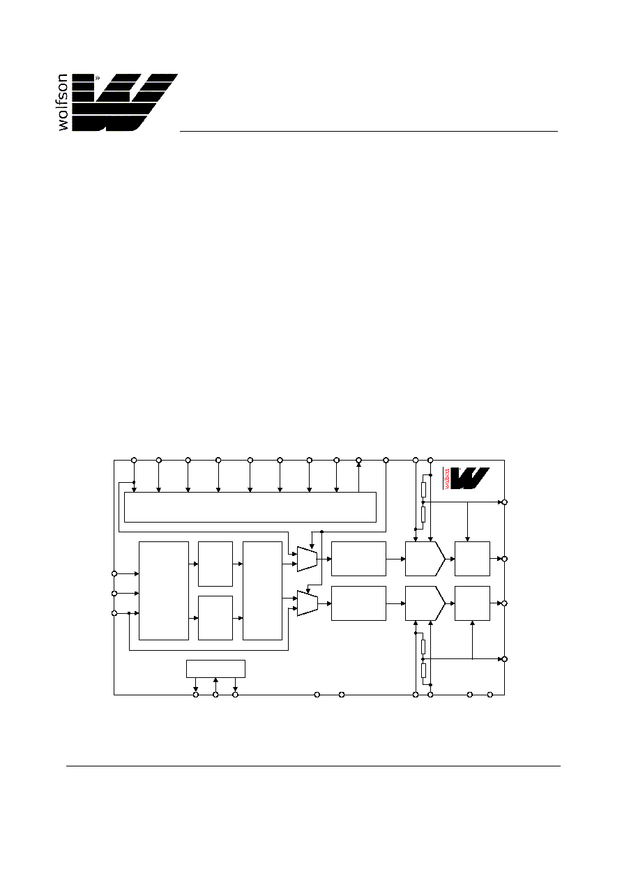
BLOCK DIAGRAM
SERIAL
INTERFACE
MUTE/
ATTEN
CONTROL INTERFACE
BCKIN (3)
(16) VOUTL
(13) VOUTR
SIGMA
DELTA
MODULATOR
LRCIN (1)
DIN (2)
AGNDR
(10)
AVDDR
(9)
MUTE/
ATTEN
SIGMA
DELTA
MODULATOR
DIGITAL
FILTERS
MODE8X
(12)
(5)
XTI
(6)
XTO
(4)
CLKO
MUX
(8)
DVDD
(15)
AVDD
(14)
AGND
(7)
DGND
MUTEB
(25)
DIFFHW
(17)
MD/DM0
(26)
MC/DM1
(27)
ML/I2S
(28)
MODE
(24)
CSBIWO
(23)
RSTB
(22)
ZERO
(21)
LOW
PASS
FILTER
LOW
PASS
FILTER
(11) VMIDR
MUX
(18) VMIDL
CRYSTAL/OSC
RIGHT
DAC
LEFT
DAC
(19)
AGNDL
(20)
AVDDL
.
WM8716
WM8716
Production Data
WOLFSON MICROELECTRONICS LTD
PD Rev 3.1 April 2001
2
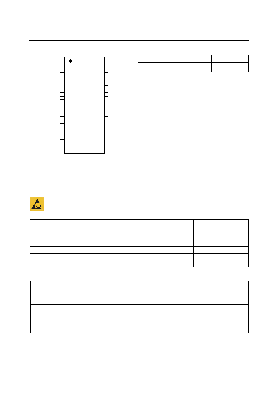
PIN CONFIGURATION
ORDERING INFORMATION
DEVICE
TEMP. RANGE
PACKAGE
WM8716EDS
-25 to +85
�
C
28-pin SSOP
16
15
14
20
19
18
17
5
6
7
1
2
3
4
13
12
11
8
9
10
BCKIN
VOUTR
VOUTL
LRCIN
DIN
ZERO
MUTEB
MODE
RSTB
CSBIWO
MD/DM0
MC/DM1
ML/I2S
VMIDR
VMIDL
XTI
XTO
CLKO
AGNDR
AGNDL
AVDDR
DVDD
AVDDL
DGND
21
22
23
24
25
26
27
28
MODE8X
AGND
DIFFHW
AVDD
ABSOLUTE MAXIMUM RATINGS
Absolute Maximum Ratings are stress ratings only. Permanent damage to the device may be caused by continuously operating at
or beyond these limits. Device functional operating limits and guaranteed performance specifications are given under Electrical
Characteristics at the test conditions specified.
ESD Sensitive Device. This device is manufactured on a CMOS process. It is therefore generically susceptible
to damage from excessive static voltages. Proper ESD precautions must be taken during handling and storage
of this device.
CONDITION
MIN
MAX
Supply voltage
-0.3V
+7.0V
Reference input
VDD + 0.3V
Operating temperature range, T
A
-25
�
C
+85
�
C
Storage temperature
-65
�
C
+150
�
C
Package body temperature (soldering, 10 seconds)
+240
�
C
Package body temperature (soldering, 2 minutes)
+183
�
C
RECOMMENDED OPERATING CONDITIONS
PARAMETER
SYMBOL
TEST CONDITIONS
MIN
TYP
MAX
UNIT
Digital supply range
DVDD
-10%
3.3 to 5
+10%
V
Analogue supply range
AVDD
-10%
3.3 to 5
+10%
V
Ground
AGND, DGND
0
V
Difference DGND to AGND
-0.3
0
+0.3
V
Analogue supply current
AVDD = 5V
26
40
mA
Digital supply current
DVDD = 5V
22
35
mA
Analogue supply current
AVDD = 3.3V
25
mA
Digital supply current
DVDD = 3.3V
13
mA
Production Data
WM8716
WOLFSON MICROELECTRONICS LTD
PD Rev 3.1 April 2001
3
ELECTRICAL CHARACTERISTICS
TEST CONDITIONS
AVDD, DVDD = 5V, AGND, DGND = 0V, T
A
= +25
o
C, fs = 48kHz, SCKI = 256fs unless otherwise stated.
PARAMETER
SYMBOL
TEST CONDITIONS
MIN
TYP
MAX
UNIT
DAC Circuit Specifications
SNR (See Notes 1 and 2)
105
112
dB
THD (full-scale)
0dB FS
-92
dB
(See Note 2)
-1dB FS
-97
dB
Dynamic range
(See Note 2)
THD @ -60dB FS
105
112
dB
Filter Characteristics (Sharp Roll-off)
Passband
�
0.0012 dB
0.4535fs
dB
Stopband
-3dB
0.491fs
Passband ripple
�
0.0012
dB
Stopband Attenuation
f > 0.5465fs
-82
dB
Delay time
30/fs
s
Filter Characteristics (Slow Roll-off)
Passband
�
0.001dB
0.274fs
Stopband
-3dB
0.459fs
Passband ripple
�
0.001
dB
Stopband Attenuation
f > 0.732fs
-82
dB
Delay time
9/fs
s
Internal Analogue Filter
Bandwidth
-3dB
195
kHz
Passband edge response
20kHz
-0.043
dB
Digital Logic Levels
Input LOW level
V
IL
0.8
Input HIGH level
(See Note 3)
V
IH
2.0
V
Output LOW level
V
OL
I
OL
= 2mA
AVSS + 0.3V
V
Output HIGH level
V
OH
I
OH
= 2mA
AVDD - 0.3V
Notes:
1.
Ratio of output level with 1kHz full scale input, to the output level with all zeros into the digital input, measured `A'
weighted over a 20Hz to 20kHz bandwidth.
2.
All performance measurements done with 20kHz low pass filter. Failure to use such a filter will result in higher THD+N and
lower SNR and Dynamic Range readings than are found in the Electrical Characteristics. The low pass filter removes out
of band noise; although it is not audible it may affect dynamic specification values.
3.
Except for Pin 12 (MODE8X) and Pin 17 (DIFFHW), where V
IH
= 2.6V min.
TERMINOLOGY
1.
Signal-to-noise ratio (dB) (SNR) is a measure of the difference in level between the full-scale output and the output with no
signal applied.
2.
Dynamic range (dB) (DNR) is a measure of the difference between the highest and lowest portions of a signal. Normally a
THD+N measurement at 60dB below full scale. The measured signal is then corrected by adding the 60dB to it. (eg
THD+N @ -60dB= -32dB, DR= 92dB).
3.
THD+N (dB) is a ratio of the r.m.s. values, of (Noise + Distortion)/Signal.
4.
Stop band attenuation (dB) is the degree to which the frequency spectrum is attenuated (outside audio band).
5.
Channel Separation (dB) (also known as Cross-Talk) is a measure of the amount one channel is isolated from the other.
Normally measured by sending a full-scale signal down one channel and measuring the other.
6.
Pass-Band Ripple - Any variation of the frequency response in the pass-band region.
WM8716
Production Data
WOLFSON MICROELECTRONICS LTD
PD Rev 3.1 April 2001
4
TEST CONDITIONS
AVDD, DVDD = 5V, AGND, DGND = 0V, T
A
= +25
o
C, fs = 48kHz, SCKI = 256fs unless otherwise stated.
PARAMETER
SYMBOL
TEST CONDITIONS
MIN
TYP
MAX
UNIT
Analogue Output Levels
Into 10kohm, full scale 0dB,
(5V supply)
1.1
V
RMS
Output level
Into 10kohm, full scale 0dB,
(3.3V supply)
0.72
V
RMS
To midrail or AC coupled
(5V supply)
1
kohms
Minimum resistance load
To midrail or AC coupled
(3.3V supply)
600
ohms
Maximum capacitance load
5V or 3.3V
100
pF
Output DC level
AVDD/2
V
Gain mismatch channel to
channel
0.5
2
%FSR
Reference Levels
Potential divider resistance
AVDD to VMIDL/VMIDR and
VMIDL/VMIDR to AGND
10
kohms
Voltage at VMIDL/VMIDR
AVSS/2
POR
POR threshold
2.5V
V
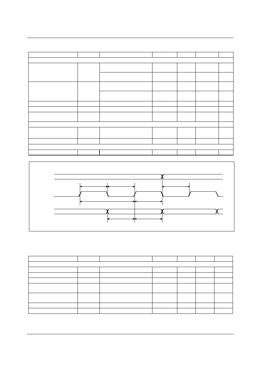
BCKIN
DIN
LRCIN
t
BCH
t
BCL
t
BL
t
LB
t
BCY
t
DS
t
DH
Figure 1 Audio Data Input Timing
TEST CONDITIONS
AVDD, DVDD = 5V, AGND, DGND = 0V, T
A
= +25
o
C, fs = 48kHz, SCKI = 256fs unless otherwise stated.
PARAMETER
SYMBOL
TEST CONDITIONS
MIN
TYP
MAX
UNIT
Audio Data Input Timing Information
BCKIN pulse cycle time
t
BCY
100
ns
BCKIN pulse width high
t
BCH
50
ns
BCKIN pulse width low
t
BCL
50
ns
BCKIN rising edge
to LRCIN edge
t
BL
30
ns
LRCIN rising edge
to BCKIN rising edge
t
LB
30
ns
DIN setup time
t
DS
30
ns
DIN hold time
t
DH
30
ns
Production Data
WM8716
WOLFSON MICROELECTRONICS LTD
PD Rev 3.1 April 2001
5
SCKI
t
SCKIL
t
SCKIH
Figure 2 System Clock Timing Requirements
TEST CONDITIONS
AVDD, DVDD = 5V, AGND, DGND = 0V, T
A
= +25
o
C, fs = 48kHz, SCKI = 256fs unless otherwise stated.
PARAMETER
SYMBOL
TEST CONDITIONS
MIN
TYP
MAX
UNIT
System Clock Timing Information
SCKI System clock pulse width high
t
SCKIH
13
ns
SCKI System clock pulse width low
t
SCKIL
13
ns
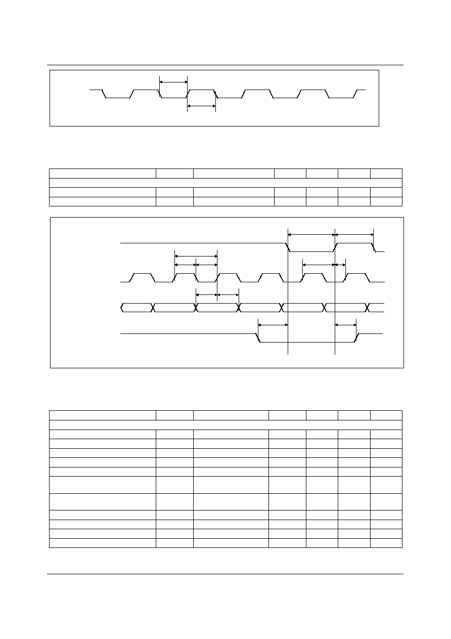
ML/I2S (PIN 28)
MC/DM1 (PIN 27)
MD/DM0 (PIN 26)
CSBIWO (PIN 23)
t
MLL
t
MHH
t
MLH
t
MCY
t
MCH
t
MCL
t
MDS
t
MDH
t
CSML
t
MLCS
LSB
t
MLS
Figure 3 Program Register Input Timing
TEST CONDITIONS
AVDD, DVDD = 5V, AGND, DGND = 0V, T
A
= +25
o
C, fs = 48kHz, SCKI = 256fs unless otherwise stated.
PARAMETER
SYMBOL
TEST CONDITIONS
MIN
TYP
MAX
UNIT
Program Register Input Information
MC/DM1 Pulse cycle time
t
MCY
100
ns
MC/DM1 Pulse width LOW
t
MCL
40
ns
MC/DM1 Pulse width HIGH
t
MCH
40
ns
MD/DM0 Hold time
t
MDH
40
ns
MD/DM0 Set-up time
t
MDS
40
ns
ML/I2S Low level time
(See Note 3)
t
MLL
40 +
1SYSCLK
ns
ML/I2S High level time
(See Note 3)
t
MHH
40 +
1SYSCLK
ns
ML/I2S Hold time
t
MLH
40
ns
ML/I2S Set-up time
t
MLS
40
ns
CSBIWO Low to ML/I2S low time
t
CSML
10
ns
ML/I2S High to CSBIWO high time
t
MLCS
10
ns
Note:
3.
System clock cycle.