Document Outline
- WM8718
- 24 Bit Differential Stereo DAC with Volume Control
- DESCRIPTION
- FEATURES
- APPLICATIONS
- BLOCK DIAGRAM
- PIN CONFIGURATION
- ORDERING INFORMATION
- PIN DESCRIPTION
- ABSOLUTE MAXIMUM RATINGS
- DC ELECTRICAL CHARACTERISTICS
- ELECTRICAL CHARACTERISTICS
- TERMINOLOGY
- MASTER CLOCK TIMING
- DIGITAL AUDIO INTERFACE TIMINGS
- 3-WIRE SERIAL CONTROL INTERFACE TIMING
- DEVICE DESCRIPTION
- INTRODUCTION
- CLOCKING SCHEMES
- DIGITAL AUDIO INTERFACE
- AUDIO DATA SAMPLING RATES
- SOFTWARE CONTROL INTERFACE
- REGISTER MAP
- DIGITAL FILTER CHARACTERISTICS
- DAC FILTER RESPONSES
- DIGITAL DE-EMPHASIS CHARACTERISTICS
- TYPICAL PERFORMANCE
- RECOMMENDED EXTERNAL COMPONENTS
- RECOMMENDED EXTERNAL COMPONENTS VALUES
- RECOMMENDED ANALOGUEUE LOW PASS FILTER FOR PCM DATA FORMAT (OPTIONAL)
- PACKAGE DIMENSIONS
- IMPORTANT NOTICE

WM8718
24 Bit Differential Stereo DAC with Volume Control
WOLFSON MICROELECTRONICS plc
www.wolfsonmicro.com
Product Preview, January 2003, Rev 1.7
Copyright
2003 Wolfson Microelectronics plc
DESCRIPTION
The WM8718 is a high performance differential stereo DAC
designed for audio applications such as DVD, home theatre
systems and digital TV. The WM8718 supports PCM data
input word lengths from 16 to 32-bits and sampling rates up
to 192kHz. The WM8718 consists of a serial interface port,
digital interpolation filters, multi-bit sigma delta modulators
and differential stereo DAC in a small 20-pin SSOP
package.
The WM8718 includes a digitally controllable
mute, an attenuate function and zero flag output for each
channel.
The 3-wire serial control port provides access to a wide
range of features including on-chip mute, attenuation and
phase reversal.
The WM8718 is an ideal device to interface to AC-3
•,
DTS
•, and MPEG audio decoders for surround sound
applications, or for use in DVD players including those
supporting DVD-A.
FEATURES
∑
24 bit Stereo DAC
∑
Fully Differential Voltage Outputs
∑
Audio Performance
-
111dB SNR (`A' weighted @ 48kHz) DAC
-
-100dB THD
∑
DAC Sampling Frequency: 8kHz - 192kHz
∑
3 Wire Serial Control Interface
∑
Programmable Audio Data Interface Modes
-
I
2
S, Left, Right Justified, DSP
-
16/20/24/32 bit Word Lengths
∑
Independent Digital Volume Control on Each Channel with
127.5dB Range in 0.5dB Steps
∑
Independent Zero Flag Outputs
∑
3.0V - 5.5V Supply Operation
∑
20-pin SSOP Package
APPLICATIONS
∑
CD, DVD, and DVD-Audio Players
∑
Home theatre systems
∑
Professional mixing desks
BLOCK DIAGRAM
AUDIO
INTERFACE
ATT/
MUTE
CONTROL
INTERFACE
BCKIN
VOUTLN
VOUTRN
SIGMA
DELTA
MODULATOR
LRCIN
DIN
ATT/
MUTE
SIGMA
DELTA
MODULATOR
DIGITAL
FILTERS
MCLK
SC
LK
SD
IN
LAT
C
H
VMID
DAC
DAC
VR
E
F
N
VR
E
F
P
VOUTRP
VOUTLP
ZEROFL
ZEROFR
AG
N
D
AV
D
D
DG
ND
DV
D
D
W
WM8718

WM8718
Product Preview
w
PP Rev 1.7 January 2003
2
PIN CONFIGURATION
ORDERING INFORMATION
DEVICE
TEMP. RANGE
PACKAGE
WM8718EDS
-25 to +85
o
C
20-pin SSOP
WM8718SEDS
-25 to +85
o
C
20-pin SSOP
(lead free)
WM8718EDS/R
-25 to +85
o
C
20-pin SSOP
(tape and reel)
WM8718SEDS/R
-25 to +85
o
C
20-pin SSOP
(lead free, tape
and reel)
SCLK
SDIN
ZEROFR
DIN
AGND
DGND
LRCIN
VOUTLP
VOUTLN
LATCH
VOUTRN
WM8718
16
15
14
20
19
18
17
5
6
7
1
2
3
4
VMID
VREFP
AVDD
DVDD
13
12
11
8
9
10
VOUTRP
MCLK
BCKIN
VREFN
ZEROFL
Note:
Reel quantity = 2,000
PIN DESCRIPTION
PIN
NAME
TYPE
DESCRIPTION
1
LRCIN
Digital Input
PCM DAC Sample Rate Clock Input
2
DVDD
Supply
Positive Digital Supply
3
DGND
Supply
Ground Digital Supply
4
AVDD
Supply
Positive Analogue Supply
5
VREFP
Supply
Positive DAC reference Supply
6
VREFN
Supply
Negative DAC reference Supply
7
AGND
Supply
Ground Analogue Supply
8
VMID
Analogue Output
Mid Rail Decoupling Point
9
VOUTRN
Analogue Output
Right Channel DAC Output Negative
10
VOUTRP
Analogue Output
Right Channel DAC Output Positive
11
VOUTLP
Analogue Output
Left Channel DAC Output Positive
12
VOUTLN
Analogue Output
Left Channel DAC Output Negative
13
LATCH
Digital Input P.U.
Serial Control Load Input
14
SDIN
Digital Input
Serial Control Data Input
15
SCLK
Digital Input P.D.
Serial Control Data Input Clock
16
ZEROFR
Digital Output (Open drain) P.D.
Infinite ZERO Detect Flag for Right Channel
17
ZEROFL
Digital Output (Open drain) P.D.
Infinite ZERO Detect Flag for Left Channel
18
MCLK
Digital Input
Master Clock Input
19
BCLKIN
Digital Input
PCM Audio Data Bit Clock Input
20
DIN
Digital Input
PCM Serial Audio Data Input
Note:
Digital input pins have Schmitt trigger input buffers. Pins marked `P.U.` or `P.D.` have an internal pull-up or pull-down resistor.

WM8718
Product Preview
w
PP Rev 1.7 January 2003
3
ABSOLUTE MAXIMUM RATINGS
Absolute Maximum Ratings are stress ratings only. Permanent damage to the device may be caused by continuously operating at
or beyond these limits. Device functional operating limits and guaranteed performance specifications are given under Electrical
Characteristics at the test conditions specified.
ESD Sensitive Device. This device is manufactured on a CMOS process. It is therefore generically susceptible
to damage from excessive static voltages. Proper ESD precautions must be taken during handling and storage
of this device.
The WM8718 has been classified as MSL1, which has an unlimited floor life at <30
o
C / 85% Relative Humidity and therefore will
not be supplied in moisture barrier bags.
CONDITION
MIN
MAX
Digital supply voltage (DVDD)
-0.3V
+7V
Analogue supply voltage (AVDD)
-0.3V
+7V
Voltage range digital inputs
DGND -0.3V
VDD +0.3V
Master Clock Frequency
37MHz
Operating temperature range, T
A
-25
∞
C
+85
∞
C
Storage temperature prior to soldering
30
∞
C max / 85% RH max
Storage temperature after soldering
-65
∞
C
+150
∞
C
Package body temperature (soldering 10 seconds)
+260
∞
C
Package body temperature (soldering 2 minutes)
+183
∞
C
WM8718
Product Preview
w
PP Rev 1.7 January 2003
4
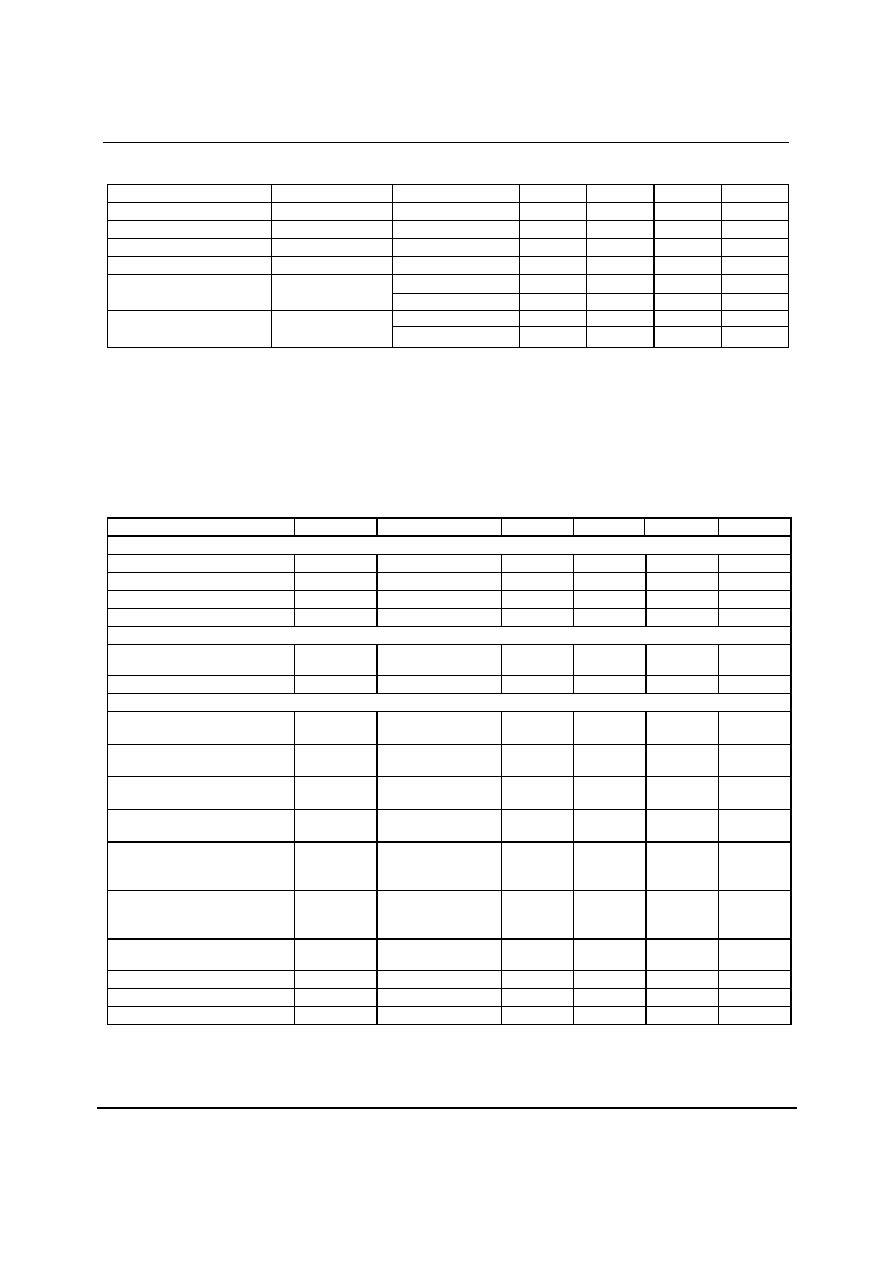
DC ELECTRICAL CHARACTERISTICS
PARAMETER
SYMBOL
TEST CONDITIONS
MIN
TYP
MAX
UNIT
Digital supply range
DVDD
3.0
5.5
V
Analogue supply range
AVDD
3.0
5.5
V
Ground
AGND, DGND
0
V
Difference DGND to AGND
-0.3
0
+0.3
V
AVDD = 3.3V
0.191
a
19
mA
Supply current
AVDD = 5V
0.191
a
22
mA
DVDD = 3.3V
160 uA
7.1
mA
Supply current
DVDD = 5V
160 uA
8.3
mA
Notes:
1.
This value represents the current usage when there are no switching digital inputs, MCLK is applied and the chip is in
power down mode
2.
Digital supply DVDD must never be more than 0.3V greater than AVDD.
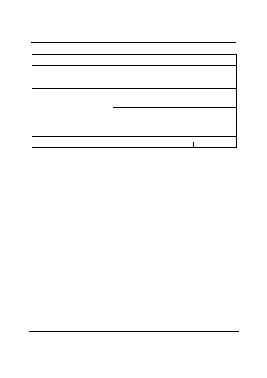
ELECTRICAL CHARACTERISTICS
Test Conditions
AVDD = 5V, DVDD = 3.3V, AGND, DGND = 0V, T
A
= +25
o
C, fs = 48kHz, MCLK = 256fs unless otherwise stated.
PARAMETER
SYMBOL
TEST CONDITIONS
MIN
TYP
MAX
UNIT
Digital Logic Levels (TTL Levels)
Input LOWlevel
V
IL
0.8
V
Input HIGH level
V
IH
2.0
V
Output LOWV
OL
I
OL
= 1mA
AGND + 0.3V
V
Output HIGH
V
OH
I
OH
= 1mA
DVDD ≠ 0.3V
V
Analogue Reference Levels
Reference voltage
VMID
AVDD/2 -
50mV
AVDD/2
AVDD/2 +
50mV
V
Potential divider resistance
R
VMID
8.7k
Ohms
DAC Output (Load = 10k ohms. 50pF)
0dBFs Full scale output voltage
At DAC outputs
2 x
AVDD/5
Vrms
SNR (Note 1,2,3)
A-weighted,
@ fs = 48kHz
106
111
dB
SNR (Note 1,2,3)
A-weighted
@ fs = 96kHz
109
dB
SNR (Note 1,2,3)
A-weighted
@ fs = 192kHz
109
dB
SNR (Note 1,2,3)
A-weighted,
@ fs = 48kHz
AVDD = 3.3V
105
dB
SNR (Note 1,2,3)
A-weighted
@ fs = 96kHz
AVDD = 3.3V
102
dB
SNR (Note 1,2,3)
Non `A' weighted @ fs
= 48kHz
108
dB
THD (Note 1,2,3)
1kHz, 0dBFs
-90
-100
dB
THD+N (Dynamic range, Note 2)
1kHz, -60dBFs
100
111
dB
DAC channel separation
100
dB
WM8718
Product Preview
w
PP Rev 1.7 January 2003
5
Test Conditions
AVDD = 5V, DVDD = 3.3V, AGND, DGND = 0V, T
A
= +25
o
C, fs = 48kHz, MCLK = 256fs unless otherwise stated.
PARAMETER
SYMBOL
TEST CONDITIONS
MIN
TYP
MAX
UNIT
Analogue Output Levels
Load = 10k Ohms,
0dBFS
2.2
V
RMS
Differential Output level
Load = 10k Ohms,
0dBFS,
(AVDD = 3.3V)
1.45
V
RMS
Gain mismatch
channel-to-channel
±1
%FSR
To midrail or a.c.
coupled
1
kohms
Minimum resistance load
To midrail or a.c.
coupled
(AVDD = 3.3V)
600
ohms
Maximum capacitance load
5V or 3.3V
100
pF
Output d.c. level
(AVDD-
GND)/2
V
Power On Reset (POR)
POR threshold
2.0
V
Notes:
1.
Ratio of output level with 1kHz full scale input, to the output level with all ZEROS into the digital input, over a 20Hz to
20kHz bandwidth.
2.
All performance measurements done with 20kHz low pass filter, and where noted an A-weight filter. Failure to use such a
filter will result in higher THD+N and lower SNR and Dynamic Range readings than are found in the Electrical
Characteristics. The low pass filter removes out of band noise; although it is not audible it may affect dynamic specification
values.
3.
VMID decoupled with 10uF and 0.1uF capacitors (smaller values may result in reduced performance).
TERMINOLOGY
1.
Signal-to-noise ratio (dB) - SNR is a measure of the difference in level between the full-scale output and the output with a
ZERO signal applied. (No Auto-ZERO or Automute function is employed in achieving these results).
2.
Dynamic range (dB) - DNR is a measure of the difference between the highest and lowest portions of a signal. Normally a
THD+N measurement at 60dB below full scale. The measured signal is then corrected by adding the 60dB to it. (e.g.
THD+N @ -60dB= -32dB, DR= 92dB).
3.
THD+N (dB) - THD+N is a ratio, of the rms values, of (Noise + Distortion)/Signal.
4.
Stop band attenuation (dB) - Is the degree to which the frequency spectrum is attenuated (outside audio band).
5.
Channel Separation (dB) - Also known as Cross Talk. This is a measure of the amount one channel is isolated from the
other. Normally measured by sending a full-scale signal down one channel and measuring the other.
6.
Pass-Band Ripple ≠ Any variation of the frequency response in the pass-band region.