Document Outline
- WM8719
- 24 Bit Differential Stereo DAC with Volume Control
- DESCRIPTION
- FEATURES
- APPLICATIONS
- BLOCK DIAGRAM
- TABLE OF CONTENTS
- PIN CONFIGURATION
- ORDERING INFORMATION
- PIN DESCRIPTION
- ABSOLUTE MAXIMUM RATINGS
- DC ELECTRICAL CHARACTERISTICS
- ELECTRICAL CHARACTERISTICS
- MASTER CLOCK TIMING
- PCM DIGITAL AUDIO INTERFACE TIMINGS
- DSD AUDIO INTERFACE TIMINGS
- MPU 3-WIRE INTERFACE TIMING
- DEVICE DESCRIPTION
- INTRODUCTION
- CLOCKING SCHEMES
- DSD MODE
- DSD <->PCM MODE SWITCHING
- PCM DIGITAL AUDIO INTERFACE
- AUDIO DATA SAMPLING RATES
- SOFTWARE CONTROL INTERFACE
- REGISTER MAP
- DIGITAL FILTER CHARACTERISTICS
- SACD FILTER CHARACTERISTICS
- DAC FILTER RESPONSES
- DIGITAL DE-EMPHASIS CHARACTERISTICS
- DSD MODE CHARACTERISTICS
- TYPICAL PERFORMANCE
- APPLICATIONS INFORMATION
- RECOMMENDED EXTERNAL COMPONENTS (PCM/DSD SLAVE MODE)
- RECOMMENDED EXTERNAL COMPONENTS VALUES
- RECOMMENDED EXTERNAL COMPONENTS (PCM/DSD MASTER MODE)
- RECOMMENDED EXTERNAL COMPONENTS VALUES
- RECOMMENDED ANALOGUE LOW PASS FILTER FOR PCM DATA FORMAT (OPTIONAL)
- PACKAGE DIMENSIONS
- IMPORTANT NOTICE

WM8719
24 Bit Differential Stereo DAC with Volume Control
WOLFSON MICROELECTRONICS plc
www.wolfsonmicro.com
Preliminary Technical Data, August 2003, Rev2.0
Copyright
2003 Wolfson Microelectronics plc
DESCRIPTION
The WM8719 is a high performance differential stereo DAC
designed for audio applications such as SACD, DVD, home
theatre systems, and digital TV. The WM8719 supports
PCM data input word lengths from 16 to 32-bits and
sampling rates up to 192kHz. Additionally 64x DSD
bitstream support is offered on both channels. The WM8719
consists of a serial interface port, digital interpolation filters,
multi-bit sigma delta modulators and differential stereo DAC
in a small 28-pin SSOP package. The WM8719 also
includes a digitally controllable mute and attenuate function
for each channel, accessible during PCM mode. A MUX is
provided to select between PCM and DSD audio data input
formats.
The 3 wire MPU serial port provides access to a wide range
of features including on-chip mute, attenuation and phase
reversal.
The WM8719 is an ideal device to interface to AC-3
,
DTS
, and MPEG audio decoders for surround sound
applications, or for use in DVD players including those
supporting DVD-A and SACD formats.
FEATURES
�
24 bit Stereo DAC
�
Fully Differential Voltage Outputs
�
Audio Performance
-
111dB SNR (`A' weighted @ 48kHz) DAC
-
-100dB THD
�
DAC Sampling Frequency: 8kHz - 192kHz
�
3 Wire Serial Control Interface
�
Programmable PCM Audio Data Interface Modes
-
I
2
S, Left, Right Justified, DSP
-
16/20/24/32 bit Word Lengths
�
Independent Digital Volume Control on Each Channel with
127.5dB Range in 0.5dB Steps (in PCM mode)
�
Independent Zero Flag Outputs
�
On board MUX to select between PCM and DSD inputs
�
Master or slave operation with Normal or Phase modulated
method of DSD data transfer
�
3.0V - 5.5V Supply Operation
�
28-pin SSOP Package
APPLICATIONS
�
CD, SACD, DVD, DVD-Audio and DVD `Universal' Players
�
Home theatre systems
�
Professional mixing desks
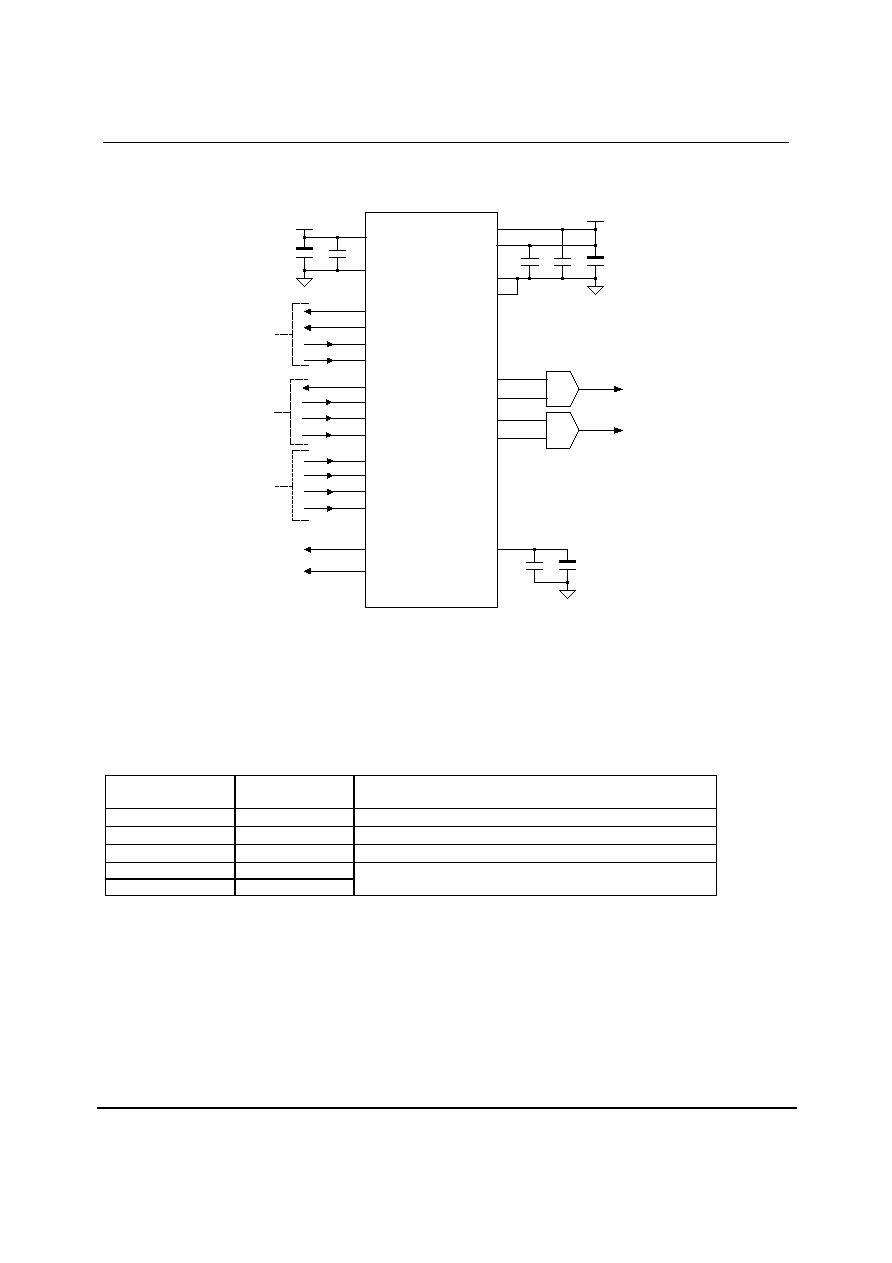
BLOCK DIAGRAM
SERIAL
INTERFACE
MUTE
CONTROL
INTERFACE
BCKIN
VOUTLN
VOUTRN
SIGMA
DELTA
MODULATOR
LRCIN
DIN
MUTE
SIGMA
DELTA
MODULATOR
DIGITAL
FILTERS
MCLK
SCLK
SDIN
LATCH
VMID
RIGHT
DAC
LEFT
DAC
VREFP
VREFP
WM8719
VOUTRP
VOUTLP
ZEROFL
ZEROFR
MUX
MUX
PCM/DSD
PCM/DSD
DSD DATA
INTERFACE
DSDCLK64
DSDCLK128
DSDL
DSDR
AGND
DGND
DVDD
AVDD
W
SDOUT

WM8719
Preliminary Technical Data
w
PTD Rev 2.0 August 2003
2
TABLE OF CONTENTS
DESCRIPTION............................................................................................................1
FEATURES..................................................................................................................1
APPLICATIONS ..........................................................................................................1
BLOCK DIAGRAM ......................................................................................................1
PIN CONFIGURATION................................................................................................3
ORDERING INFORMATION .......................................................................................3
PIN DESCRIPTION .....................................................................................................4
ABSOLUTE MAXIMUM RATINGS ..............................................................................5
DC ELECTRICAL CHARACTERISTICS .....................................................................6
ELECTRICAL CHARACTERISTICS ...........................................................................6
TERMINOLOGY ................................................................................................................. 7
MASTER CLOCK TIMING .................................................................................................. 8
PCM DIGITAL AUDIO INTERFACE TIMINGS.................................................................... 8
DSD AUDIO INTERFACE TIMINGS................................................................................... 9
MPU 3-WIRE INTERFACE TIMING ..................................................................................11
DEVICE DESCRIPTION............................................................................................12
INTRODUCTION ...............................................................................................................12
CLOCKING SCHEMES .....................................................................................................12
DSD MODE .......................................................................................................................13
DSD <-> PCM MODE SWITCHING...................................................................................13
PCM DIGITAL AUDIO INTERFACE ..................................................................................14
AUDIO DATA SAMPLING RATES.....................................................................................17
SOFTWARE CONTROL INTERFACE...............................................................................17
REGISTER MAP ...............................................................................................................19
DIGITAL FILTER CHARACTERISTICS.............................................................................26
SACD FILTER CHARACTERISTICS.................................................................................26
DAC FILTER RESPONSES...............................................................................................26
DIGITAL DE-EMPHASIS CHARACTERISTICS ........................................................27
DSD MODE CHARACTERISTICS.....................................................................................28
TYPICAL PERFORMANCE.......................................................................................29
APPLICATIONS INFORMATION ..............................................................................30
RECOMMENDED EXTERNAL COMPONENTS (PCM/DSD SLAVE MODE) ....................30
RECOMMENDED EXTERNAL COMPONENTS VALUES .................................................30
RECOMMENDED EXTERNAL COMPONENTS (PCM/DSD MASTER MODE) .................31
RECOMMENDED EXTERNAL COMPONENTS VALUES .................................................31
RECOMMENDED ANALOGUE LOW PASS FILTER FOR PCM DATA FORMAT
(OPTIONAL)......................................................................................................................32
PACKAGE DIMENSIONS .........................................................................................33
IMPORTANT NOTICE ...............................................................................................34
ADDRESS: ........................................................................................................................34
WM8719
Preliminary Technical Data
w
PTD Rev 2.0 August 2003
3
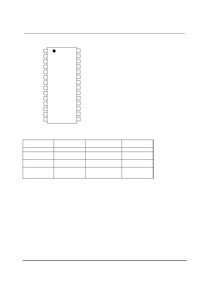
PIN CONFIGURATION
WM8719
1
LRCLK
2
VOUTLP
3
BCLK
4
MCLK
5
DIN
6
VOUTLN
7
8
SDOUT
9
10
DSDCLK128
DSDL
DSDCLK64
DSDR
15
VREFP
ZEROFL
DVSS
AVDD
SCLK
SDIN
LATCH
DVDD
AVSS
ZEROFR
VREFN
VMID
VOUTRN
VOUTRP
11
12
13
14
16
17
18
19
20
21
22
23
24
25
28
27
26
NC
NC
NC
ORDERING INFORMATION
DEVICE
TEMP. RANGE
PACKAGE
MOISTURE
SENSITIVITY LEVEL
WM8719EDS
-25 to +85
o
C
28-pin SSOP
MSL1
WM8719SEDS
-25 to +85
o
C
28-pin SSOP
(lead free)
MSL1
WM8719EDS/R
-25 to +85
o
C
28-pin SSOP
(tape and reel)
MSL1
WM8719SEDS/R
-25 to +85
o
C
28-pin SSOP
(lead free, tape
and reel)
MSL1
Note:
Reel quantity = 2,000

WM8719
Preliminary Technical Data
w
PTD Rev 2.0 August 2003
4
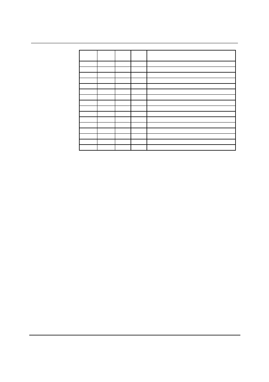
PIN DESCRIPTION
PIN
NAME
TYPE
DESCRIPTION
1
LRCIN
Digital Input
PCM DAC Sample Rate Clock Input
2
LATCH
Digital Input P.U.
Serial Control Load Input
3
SCLK
Digital Input P.D.
Serial Control Data Input Clock
4
SDIN
Digital
Serial Control Data Input
5
DVDD
Supply
Digital Positive Supply
6
DGND
Supply
Digital Ground Supply
7
AVDD
Supply
Analog Ground Supply
8
VREFP
Supply
DAC Positive Reference
9
VREFN
Supply
DAC Negative Reference
10
AGND
Supply
Analog Ground Supply
11
VMID
Analogue Output
Mid Rail Decoupling Point
12
ZEROFR
Digital Output (Open drain) P.D. Infinite ZERO Detect Flag for Right Channel
13
VOUTRN
Analogue Output
Right Channel DAC Output Positive
14
VOUTRP
Analogue Output
Right Channel DAC Output Negative
15
VOUTLP
Analogue Output
Left Channel DAC Output Positive
16
VOUTLN
Analogue Output
Left Channel DAC Output Negative
17
ZEROFL
Digital Output (Open drain) P.D. Infinite ZERO Detect Flag for Right Channel
18
NC
19
NC
20
DSDR
Digital Input
Right channel DSD Bitstream input
21
DSDL
Digital Input
Left channel DSD Bitstream input
22
DSDCLK64
Digital Bi-directional P.D.
DSD format clock at 64fs.
23
DSDCLK128
Digital Bi-directional P.D.
DSD format clock at 128fs. (Optional for DSD Bi-phase mode)
24
NC
25
SDOUT
Digital Output
Serial Control Data Output
26
MCLK
Digital Input
Master Clock Input
27
BCLKIN
Digital Input
PCM Audio Data Bit Clock Input
28
DIN
Digital Input
PCM Serial Audio Data Input
Note:
1.
Digital input pins have Schmitt trigger input buffers. Pins marked `P.U.` or `P.D.` have a internal pull-up or pull-down.
WM8719
Preliminary Technical Data
w
PTD Rev 2.0 August 2003
5
ABSOLUTE MAXIMUM RATINGS
Absolute Maximum Ratings are stress ratings only. Permanent damage to the device may be caused by continuously operating at
or beyond these limits. Device functional operating limits and guaranteed performance specifications are given under Electrical
Characteristics at the test conditions specified.
ESD Sensitive Device. This device is manufactured on a CMOS process. It is therefore generically susceptible
to damage from excessive static voltages. Proper ESD precautions must be taken during handling and storage
of this device.
Wolfson tests its package types according to IPC/JEDEC J-STD-020A for Moisture Sensitivity to determine acceptable storage
conditions prior to surface mount assembly. These levels are:
MSL1 = unlimited floor life at <30
�
C / 85% Relative Humidity. Not normally stored in moisture barrier bag.
MSL2 = out of bag storage for 1 year at <30
�
C / 60% Relative Humidity. Supplied in moisture barrier bag.
MSL3 = out of bag storage for 168 hours at <30
�
C / 60% Relative Humidity. Supplied in moisture barrier bag.
The Moisture Sensitivity Level for each package type is specified in Ordering Information.
CONDITION
MIN
MAX
Digital supply voltage (DVDD)
-0.3V
+7V
Analogue supply voltage (AVDD)
-0.3V
+7V
Voltage range digital inputs
DGND -0.3V
VDD +0.3V
Master Clock Frequency
37MHz
Operating temperature range, T
A
-25
�
C
+85
�
C
Storage temperature
-65
�
C
+150
�
C
Package body temperature (soldering 10 seconds), Pb and Pb free
+260
�
C
Package body temperature (soldering 2 minutes)
+183
�
C

WM8719
Preliminary Technical Data
w
PTD Rev 2.0 August 2003
6
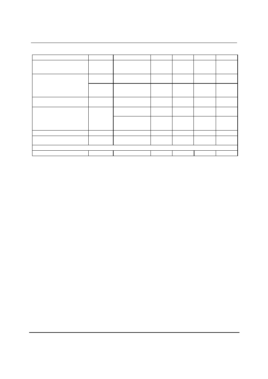
DC ELECTRICAL CHARACTERISTICS
PARAMETER
SYMBOL
TEST CONDITIONS
MIN
TYP
MAX
UNIT
Digital supply range
DVDD
3.0
5.5
V
Analogue supply range
AVDD
3.0
5.5
V
Ground
AGND, DGND
0
V
Difference DGND to AGND
-0.3
0
+0.3
V
AVDD = 3.3
16
mA
Supply current
AVDD = 5V
19
mA
DVDD = 3.3V
16
mA
Supply current
DVDD = 5V
30
mA
Notes:
1.
This value represents the current usage when there are no switching digital inputs, MCLK is applied and the chip is in
power down mode
2.
Digital supply DVDD must never be more than 0.3V greater than AVDD.
ELECTRICAL CHARACTERISTICS
Test Conditions
AVDD = 5V, DVDD = 3.3V, AGND, DGND = 0V, T
A
= +25
o
C, fs = 48kHz, MCLK = 256fs unless otherwise stated.
PARAMETER
SYMBOL
TEST CONDITIONS
MIN
TYP
MAX
UNIT
Digital Logic Levels (TTL Levels)
Input LOW level
V
IL
0.8
V
Input HIGH level
V
IH
2.0
V
Output LOW
V
OL
I
OL
= 1mA
AGND + 0.3V
V
Output HIGH
V
OH
I
OH
= 1mA
DVDD � 0.3V
V
Analogue Reference Levels
Reference voltage
VMID
AVDD/2 -
50mV
AVDD/2
AVDD/2 +
50mV
V
Potential divider resistance
R
VMID
8.7k
Ohms
DAC Output (Load
= 10k ohms. 50pF)
0dBFs Full scale output voltage
At DAC outputs
2 x
AVDD/5
Vrms
SNR (Note 1,2,3)
A-weighted,
@ fs = 48kHz
105
111
dB
SNR (Note 1,2,3)
A-weighted
@ fs = 96kHz
109
dB
SNR (Note 1,2,3)
A-weighted
@ fs = 192kHz
109
dB
SNR (Note 1,2,3)
A-weighted,
@ fs = 48kHz
AVDD = 3.3V
105
dB
SNR (Note 1,2,3)
A-weighted
@ fs = 96kHz
AVDD = 3.3V
102
dB
SNR (Note 1,2,3)
Non `A' weighted @ fs
= 48kHz
108
dB
THD (Note 1,2,3)
1kHz, 0dBFs
-80
-100
dB
THD+N (Dynamic range, Note 2)
1kHz, -60dBFs
105
111
dB
DAC channel separation
100
dB
Analogue Output Levels
Differential Output level (PCM)
Load = 10k Ohms,
0dBFS
2.2
V
RMS
WM8719
Preliminary Technical Data
w
PTD Rev 2.0 August 2003
7
Test Conditions
AVDD = 5V, DVDD = 3.3V, AGND, DGND = 0V, T
A
= +25
o
C, fs = 48kHz, MCLK = 256fs unless otherwise stated.
PARAMETER
SYMBOL
TEST CONDITIONS
MIN
TYP
MAX
UNIT
Load = 10k Ohms,
0dBFS,
(AVDD = 3.3V)
1.45
V
RMS
Load = 10k Ohms,
0dBFS
1.6
V
RMS
Differential Output level (DSD)
Load = 10k Ohms,
0dBFS,
(AVDD = 3.3V)
0.96
V
RMS
Gain mismatch
channel-to-channel
�1
%FSR
To midrail or a.c.
coupled
1
kohms
Minimum resistance load
To midrail or a.c.
coupled
(AVDD = 3.3V)
600
ohms
Maximum capacitance load
5V or 3.3V
100
pF
Output d.c. level
(AVDD-
GND)/2
V
Power On Reset (POR)
POR threshold
2.0
V
Notes:
1.
Ratio of output level with 1kHz full scale input, to the output level with all ZEROS into the digital input, over a 20Hz to
20kHz bandwidth.
2.
All performance measurements done with 20kHz low pass filter, and where noted an A-weight filter. Failure to use such a
filter will result in higher THD+N and lower SNR and Dynamic Range readings than are found in the Electrical
Characteristics. The low pass filter removes out of band noise; although it is not audible it may affect dynamic specification
values.
3.
VMID decoupled with 10uF and 0.1uF capacitors (smaller values may result in reduced performance).
TERMINOLOGY
2.
Signal-to-noise ratio (dB) - SNR is a measure of the difference in level between the full-scale output and the output with a
ZERO signal applied. (No Auto-ZERO or Automute function is employed in achieving these results).
3.
Dynamic range (dB) - DNR is a measure of the difference between the highest and lowest portions of a signal. Normally a
THD+N measurement at 60dB below full scale. The measured signal is then corrected by adding the 60dB to it. (e.g.
THD+N @ -60dB= -32dB, DR= 92dB).
4.
THD+N (dB) - THD+N is a ratio, of the rms values, of (Noise + Distortion)/Signal.
5.
Stop band attenuation (dB) - Is the degree to which the frequency spectrum is attenuated (outside audio band).
6.
Channel Separation (dB) - Also known as Cross Talk. This is a measure of the amount one channel is isolated from the
other. Normally measured by sending a full-scale signal down one channel and measuring the other.
7.
Pass-Band Ripple � Any variation of the frequency response in the pass-band region.

WM8719
Preliminary Technical Data
w
PTD Rev 2.0 August 2003
8
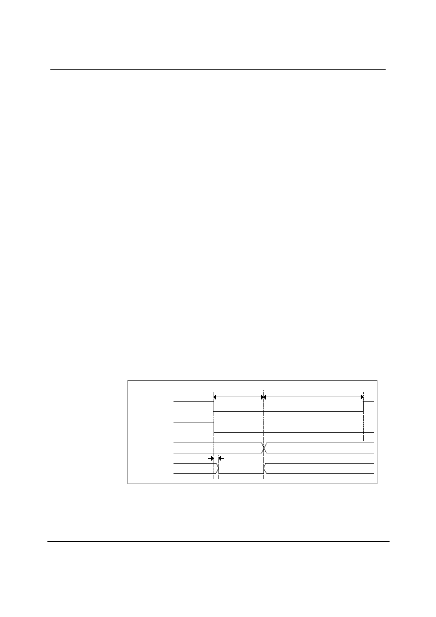
MASTER CLOCK TIMING
MCLK
t
MCLKL
t
MCLKH
t
MCLKY
Figure 1 Master Clock Timing Requirements
Test Conditions
AVDD = DVDD = 5V, AGND = DGND = 0V, T
A
= +25
o
C, fs = 48kHz, MCLK = 256fs unless otherwise stated.
PARAMETER
SYMBOL
TEST CONDITIONS
MIN
TYP
MAX
UNIT
Master Clock Timing Information
MCLK Master clock pulse width high
t
MCLKH
13
ns
MCLK Master clock pulse width low
t
MCLKL
13
ns
MCLK Master clock cycle time
t
MCLKY
26
ns
MCLK Duty cycle
40:60
60:40
PCM DIGITAL AUDIO INTERFACE TIMINGS
BCKIN
LRCIN
t
BCH
t
BCL
t
BCY
DIN
t
LRSU
t
DS
t
LRH
t
DH
Figure 2 Digital Audio Data Timing
Test Conditions
AVDD = DVDD = 5V, AGND = DGND = 0V, T
A
= +25
o
C, fs = 48kHz, MCLK = 256fs unless otherwise stated.
PARAMETER
SYMBOL
TEST CONDITIONS
MIN
TYP
MAX
UNIT
Audio Data Input Timing Information
BCKIN cycle time
t
BCY
40
ns
BCKIN pulse width high
t
BCH
16
ns
BCKIN pulse width low
t
BCL
16
ns
LRCIN set-up time to
BCKIN rising edge
t
LRSU
8
ns
LRCIN hold time from
BCKIN rising edge
t
LRH
8
ns
DIN set-up time to BCKIN
rising edge
t
DS
8
ns
DIN hold time from BCKIN
rising edge
t
DH
8
ns

WM8719
Preliminary Technical Data
w
PTD Rev 2.0 August 2003
9
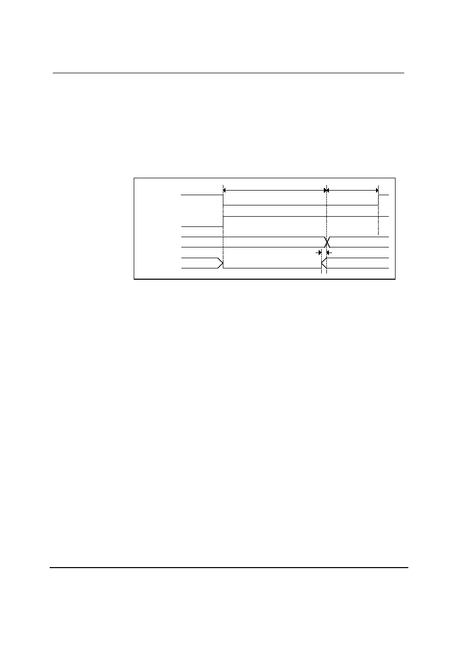
DSD AUDIO INTERFACE TIMINGS
DSDCLK64
DSD[0:1]
t
DH
t
DS
t
64L
t
64H
t
64CY
t
DC
D[n]
D[n-1]
D[n+1]
MCLK
Figure 3 DSD Audio Timing - Normal Mode Without MCLK
DSDCLK64
DSD[0:1]
MCLK/
DSDCLK128
t
DH
t
DS
t
64L
t
64H
t
64CY
t
MCLKL
t
MCLKH
t
DIFF
t
MCLKY
t
DC
D[n]
D[n-1]
D[n+1]
Figure 4 DSD Audio Timing - Normal Mode With MCLK
DSDCLK64
DSD[0:1]
MCLK/
DSDCLK128
t
DH
t
DS
t
64L
t
64H
t
64CY
t
PCLKL
t
PCLKH
t
DIFF
t
PCLKY
t
DC
D[n]
D[n-1]
D[n+1]
Inverse D[n]
Figure 5 DSD Audio Timing - Phase Modulated Mode

WM8719
Preliminary Technical Data
w
PTD Rev 2.0 August 2003
10
DSDCLK128
DSD[0:1]
D(n)
inverse D(n)
DSDCLK64
inverse D(n-1)
Figure 6 DSD Audio Timing - Master Mode Timing
Test Conditions
AVDD = DVDD = 5V, AGND = DGND = 0V, T
A
= +25
o
C, fs = 48kHz, SCKI = 256fs unless otherwise stated.
PARAMETER
SYMBOL
TEST CONDITIONS
MIN
TYP
MAX
UNIT
Audio Data Input Timing Information
DSDCLK64 cycle time
t
64CY
354.4
ns
DSDCLK128 cycle time
t
PCLKY
177.2
ns
DSDCLK64 pulse width high
t
64H
140
ns
DSDCLK64 pulse width low
t
64L
140
ns
DSD[0:1] set-up time to
DSDCLK64 rising edge
t
DSN
20
ns
DSD[0:1] hold time from
DSDCLK64 rising edge
t
DHN
20
ns
Difference in edge timing of
DSD[0:1] to DSDCLK64
t
DC
-10
10
ns
DSD[0:1] set-up time to
MCLK/DSDCLK128 falling
edge.
t
DS
20
ns
DSD[0:1] hold-up time from
MCLK/DSDCLK128 falling
edge.
t
DH
20
ns
MCLK/DSDCLK128 first
falling edge to DSDCLK64
rising edge.
t
DIFF
7
ns
Phase modulation Clock
pulse width low.
t
PCLKL
13
ns
Phase modulation Clock
pulse width high.
t
PCLKH
13
ns
Phase modulation Clock
Cycle Time
t
PCLKY
26
ns
MCLK Clock pulse width low
t
MCLKY
13
MCLK Clock pulse width
high
t
MCLKY
13
MCLK Clock Cycle Time
t
MCLKY
26
ns
WM8719
Preliminary Technical Data
w
PTD Rev 2.0 August 2003
11
MPU 3-WIRE INTERFACE TIMING
LATCH
SCLK
SDIN
t
CSL
t
DHO
t
DSU
t
CSH
t
SCY
t
SCH
t
SCL
t
SCS
D0
t
CSS
D0*
SDOUT
D15*
D14*
D15
D14
D13*
D13
Figure 7 Program Register Input Timing - 3-Wire Serial Control Mode
Test Conditions
AVDD = DVDD = 5V, AGND = DVDD = 0V, T
A
= +25
o
C, fs = 48kHz, MCLK = 256fs unless otherwise stated.
PARAMETER
SYMBOL
TEST CONDITIONS
MIN
TYP
MAX
UNIT
Program Register Input Information
SCLK rising edge to LATCH
rising edge
t
SCS
40
ns
SCLK pulse cycle time
t
SCY
80
ns
SCLK pulse width low
t
SCL
20
ns
SCLK pulse width high
t
SCH
20
ns
SDIN to SCLK set-up time
t
DSU
20
ns
SCLK to SDIN hold time
t
DHO
20
ns
LATCH pulse width low
t
CSL
20
ns
LATCH pulse width high
t
CSH
20
ns
LATCH rising to SCLK rising
t
CSS
20
ns

WM8719
Preliminary Technical Data
w
PTD Rev 2.0 August 2003
12
DEVICE DESCRIPTION
INTRODUCTION
The WM8719 is a high performance DAC designed for digital consumer audio applications. Its
range of features makes it ideally suited for use in DVD players, AV receivers and other high-end
consumer audio equipment.
WM8719 is a complete 2-channel differential stereo audio digital-to-analogue converter, including
digital interpolation filter, multi-bit sigma delta with dither, switched capacitor multi-bit stereo DAC.
The WM8719 includes an on-chip digital volume control, configurable digital audio interface and a
3 wire MPU control interface. It is fully compatible and an ideal partner for a range of industry
standard microprocessors, controllers and DSPs.
The software control interface may be asynchronous to the audio data interface. In which case
control data will be re-synchronised to the audio processing internally.
Operation using a master clock of 128fs, 192fs, 256fs, 384fs, 512fs or 768fs is provided, selection
between clock rates being automatically controlled in hardware mode, or serial controlled when in
software mode. Sample rates (fs) from less than 8ks/s to 96ks/s are allowed, provided the
appropriate master clock is input. Support is also provided for up to 192ks/s using a master clock
of 128fs or 192fs.
In normal PCM mode, the audio data interface supports right justified, left justified and I
2
S (Philips
left justified, one bit delayed) interface formats along with a highly flexible DSP serial port
interface.
In DSD mode, DSDL and DSDR are the bitstream data input pins for the left and right channels,
respectively, plus DSDCLK64 for the 64fs data clock. Additionally in DSD mode, a Phase
Modulation scheme is supported, where the audio data is transmitted as a Manchester type, bi-
phase encoded bitstream. This has the advantage of removing the significant spectral audio
spectral energy from the bitstream, so minimizing digital signal corruption of the analogue
outputs. In order to simplify decoding of this phase modulated data, a 128fs or multiple,
DSDCLK128 or MCLK, is used to sample the incoming data.
In DSD mode, clocks for the DAC can either be inputs (WM8719 in SLAVE mode) or outputs
(WM8719 in MASTER mode). When the clocks are outputs, MCLK remains an input, the lower
rates derived by dividing this master clock signal. The 64fs clock is outputted on the DSDCLK64
pin and the 128fs clock is outputted on the DSDCLK128 pin for the DSD decoding. Depending
upon the DSDCKISEL register bit, a master clock of 256fs, 384fs, 512fs and 768fs may be used
as the input, from which the DSD clocks will be derived appropriately.
The device is packaged in a small 28-pin SSOP.
CLOCKING SCHEMES
In a typical digital audio system there is only one central clock source producing a reference clock
to which all audio data processing is synchronised. This clock is often referred to as the audio
system's Master Clock. The external master system clock can be applied directly through the
MCLK input pin with no software configuration necessary for sample rate selection.
Note that on the WM8719, MCLK is used to derive clocks for the DAC path in PCM mode. The
DAC path consists of DAC sampling clock, DAC digital filter clock and DAC digital audio interface
timing. In a system where there are a number of possible sources for the reference clock it is
recommended that the clock source with the lowest jitter be used to optimise the performance of
the DAC.
WM8719
Preliminary Technical Data
w
PTD Rev 2.0 August 2003
13
DSD MODE
When the DSDMODE registry bit is set, the device is reconfigured to operate in DSD mode or
`bitstream' compatible DAC. In this mode the internal digital filters are bypassed, and the already
modulated bitstream data is applied directly to the Switched Capacitor DAC filter where it is
converted and lowpass filtered.
The WM8719 supports this mode when run at 64x the oversampling rate. That is, the data is
supplied at a rate of 64 bits per normal word clock. Of course no word clock is provided, and the
actual spectral content of the data is determined by the noise shaping that was used to create the
bitstream. The WM8719 supports 2 channels of bitstream or DSD audio. Data bitstreams and the
64fs clock are supplied to pins 20,21 and 22 respectively. The DSDMODE register bit controls the
mulitplexor, which switches the input signal to the DAC's from the audio interface (PCM) to the
DSD on the pins.
In DSD bi-phase mode the data supplied is Manchester encoded, requiring a 128fs or multiple
clock to be present on pin 23.
In DSD mode operation, the entire digital filter on the WM8719 is disabled, and the bitstream data
is applied directly to the multi-bit switched capacitor DAC's in the analogue part of the device.
It is normally desirable to use an external analogue post-DAC filter, particularly in the case of DSD
operation due to the presence of high frequency energy as a result of the aggressive high order
noise shaping used in the creation of the modulated DSD datastream.
DSD <-> PCM MODE SWITCHING
The WM8719 is designed so that its' mode of operation can be changed via the DSDMODE
registry bit. During the transition time the zero flag pins will go low so that any external muting
circuitry can mute the output while the WM8719 is changed from one mode of operation to
another.
DSD TO PCM SWITCHING
When the DSDMODE registry bit is changed from DSD mode to PCM mode, the zero flag pins
will go low. At this point any DSD data feed into the WM8719 is ignored, instead an internal
midrail signal is generated ramping the output to midrail. After 1024 periods of the DSDCLK64
Clock the WM8719 will change modes and start accepting data from the PCM data pins. If no
PCM data is provided the WM8719 will default to 768fs mode and LRCIN will be derived from the
SCLK rate. After 512 LRCIN periods the zero flag pins will go high indicating the change has
taken place. At the same time if the chip had been in DSD master mode the DSDCLK64 and
DSDCLK128 clocks will stop being outputted.
Zero Flags
DSDMODE bit
INPUT DATA
DSD DATA
PCM DATA
MODE
DSD MODE
PCM MODE
512 * LRCLK
1024 * DSDCLK64
0
Figure 8 DSD to PCM Switching Timing
WM8719
Preliminary Technical Data
w
PTD Rev 2.0 August 2003
14
PCM TO DSD SWITCHING
When the DSDMODE registry bit is changed from PCM mode to DSD mode, the zero flag pins
will go low. At this point any PCM data feed into the WM8719 is ignored, instead an internal
midrail signal is generated ramping the output down to midrail. At the same time if DSD master
mode has been selected the 64fs and 128fs clocks will be outputted, whose timing is shown in
Figure 6. If there is a 128fs clock present on pin 23 this clock will be used instead of MCLK.
Before the internal circuitry changes modes DSD data must be present on the respectable pins,
so that the transition is as smooth as possible, failure to do so will cause the output to there
respective extremes. The chip will internally change modes after 512 LRCIN periods, the LRCIN
period is determined from that last PCM data input before the zero flags go low and internally
derived off SCLK. After 1024 periods of the DSDCLK64 Clock the zero flags will go high indicating
the change has taken place.
DSD MODE
DSDMODE bit
ZEROFR pin
INPUT DATA
PCM DATA
DSD DATA
MODE
PCM MODE
1024 * DSDCLK64
512 * LRCLK
0
Figure 9 PCM to DSD Switching Timing
Note:
1. From the time that the registry write is made to change the WM8719's mode of operation both
MCLK and DSDCK64, (unless in master mode), must be present on the relevant pins until the
zero flags go high to indicate the end of the mode change over, when only the Clock(s) needed
for that mode of operation need to be present on the relevant pins. The timing diagram Figure
4 shows the relationship between MCLK and DSDCLK64 during a mode change Figure 3 show
the timing when in DSD normal mode with no MCLK running. Figure 5 show the timing for DSD
Phase modulated mode.
2. Before and during the change over of the WM8719's mode of operation it is recommended that
audio input signal should be a midrail value. This ensures that there is minimum distortion
seen on the output when the mode of the WM8719 is changed.
PCM DIGITAL AUDIO INTERFACE
Audio data is applied to the internal DAC filters via the Digital Audio Interface. Five popular
interface formats are supported:
�
Left Justified mode
�
Right Justified mode
�
I
2
S mode
�
DSP Early mode
�
DSP Late mode
All five formats send the MSB first and support word lengths of 16, 20, 24 and 32 bits with the
exception that 32 bit data is not supported in right justified mode. DIN and LRCIN maybe
configured to be sampled on the rising or falling edge of BCKIN.
WM8719
Preliminary Technical Data
w
PTD Rev 2.0 August 2003
15
In left justified, right justified and I
2
S modes, the digital audio interface receives data on the DIN
input. Audio Data is time multiplexed with LRCIN indicating whether the left or right channel is
present. LRCIN is also used as a timing reference to indicate the beginning or end of the data
words. The minimum number of BCKINs per LRCIN period is 2 times the selected word length.
LRCIN must be high for a minimum of word length BCKINs and low for a minimum of word length
BCKINs. Any mark to space ratio on LRCIN is acceptable provided the above requirements are
met
The WM8719 will automatically detect when data with a LRCIN period of exactly 32 BCKINs is
sent, and select 16-bit mode - overriding any previously programmed word length. Word length
will revert to a programmed value only if a LRCIN period other than 32 BCKINs is detected.
In DSP early or DSP late mode, the data is time multiplexed onto DIN. LRCIN is used as a frame
sync signal to identify the MSB of the first word. The minimum number of BCKINs per LRCIN
period is 2 times the selected word length. Any mark to space ratio is acceptable on LRCIN
provided the rising edge is correctly positioned. (See Figure 13 and Figure 14)
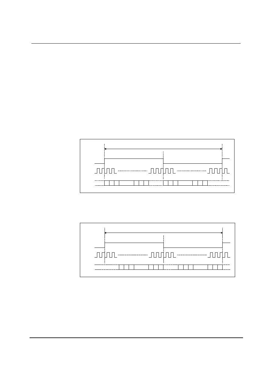
LEFT JUSTIFIED MODE
In left justified mode, the MSB is sampled on the first rising edge of BCKIN following a LRCIN
transition. LRCIN is high during the left data word and low during the right data word.
LEFT CHANNEL
RIGHT CHANNEL
LRCIN
BCKIN
DIN
1/fs
n
3
2
1
n-2 n-1
LSB
MSB
n
3
2
1
n-2 n-1
LSB
MSB
Figure 10 Left Justified Mode Timing Diagram
RIGHT JUSTIFIED MODE
In right justified mode, the LSB is sampled on the rising edge of BCKIN preceding a LRCIN
transition. LRCIN is high during the left data word and low during the right data word.
LEFT CHANNEL
RIGHT CHANNEL
LRCIN
BCKIN
DIN
1/fs
n
3
2
1
n-2 n-1
LSB
MSB
n
3
2
1
n-2 n-1
LSB
MSB
Figure 11 Right Justified Mode Timing Diagram
WM8719
Preliminary Technical Data
w
PTD Rev 2.0 August 2003
16
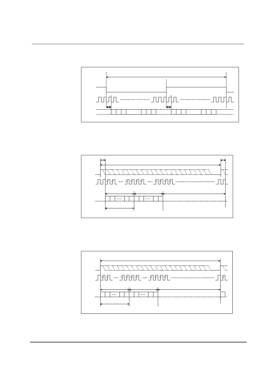
I
2
S MODE
In I
2
S mode, the MSB is sampled on the second rising edge of BCKIN following a LRCIN
transition. LRCIN is low during the left data word and high during the right data word.
LEFT CHANNEL
RIGHT CHANNEL
LRCIN
BCKIN
DIN
1/fs
n
3
2
1
n-2 n-1
LSB
MSB
n
3
2
1
n-2 n-1
LSB
MSB
1 BCKIN
1 BCKIN
Figure 12 I
2
S Mode Timing Diagram
DSP EARLY MODE
In DSP early mode, the first bit is sampled on the BCKIN rising edge following the one that
detects a low to high transition on LRCIN. No BCKIN edges are allowed between the data words.
The word order is DIN left, DIN right.
LRCIN
BCKIN
DIN
Input Word Length (IWL)
1/fs
LEFT CHANNEL
n
2
1
n-1
LSB
MSB
n
2
1
n-1
RIGHT CHANNEL
NO VALID DATA
1 BCKIN
1 BCKIN
Figure 13 DSP Early Mode Timing Diagram
DSP LATE MODE
In DSP late mode, the first bit is sampled on the BCKIN rising edge, which detects a low to high
transition on LRCIN. No BCKIN edges are allowed between the data words. The word order is
DIN left, DIN right.
LRCIN
BCKIN
DIN
Input Word Length (IWL)
1/fs
LEFT CHANNEL
n
2
1
n-1
LSB
MSB
n
2
1
n-1
RIGHT CHANNEL
NO VALID DATA
1
Figure 14 DSP Late Mode Timing Diagram
WM8719
Preliminary Technical Data
w
PTD Rev 2.0 August 2003
17
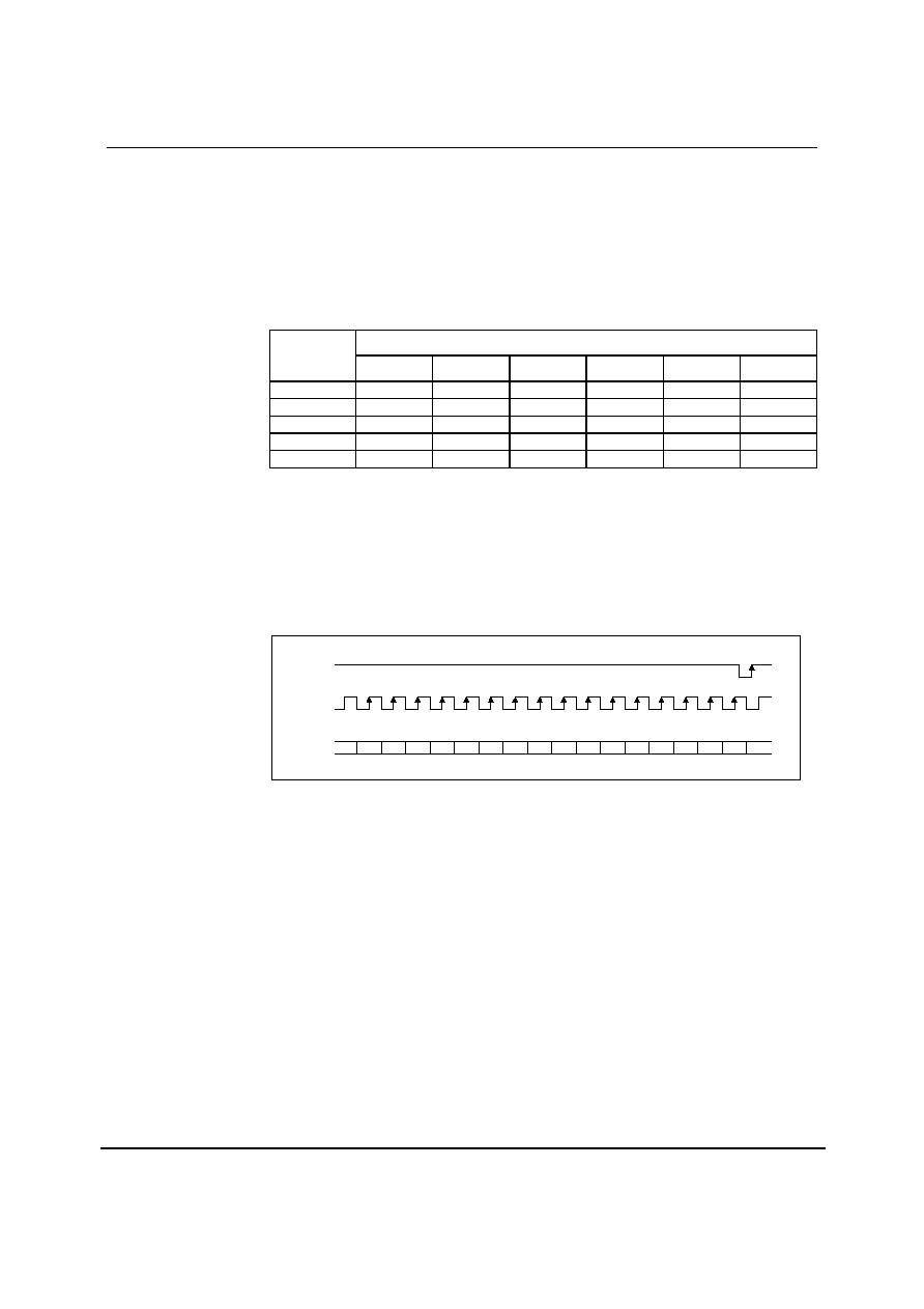
AUDIO DATA SAMPLING RATES
The master clock for WM8719 can range from 128fs to 768fs, where fs is the audio sampling
frequency (LRCIN) typically 32kHz, 44.1kHz, 48kHz, 96kHz or 192kHz. The master clock is used
to operate the digital filters and the noise shaping circuits.
The WM8719 has a master clock detection circuit that automatically determines the relationship
between the master clock frequency and the sampling rate (to within +/- 32 system clocks). If
there is a greater than 32 clocks error, the system will default to 768fs. The master clock should
be synchronised with LRCIN, although the WM8719 is tolerant of phase differences or jitter on
this clock. See Table 1.
MASTER CLOCK FREQUENCY (MHZ) (MCLK)
SAMPLING
RATE
(LRCIN)
128fs
192fs
256fs
384fs
512fs
768fs
32kHz
4.096
6.144
8.192
12.288
16.384
24.576
44.1kHz
5.6448
8.467
11.2896
16.9340
22.5792
33.8688
48kHz
6.144
9.216
12.288
18.432
24.576
36.864
96kHz
12.288
18.432
24.576
36.864
Unavailable Unavailable
192kHz
24.576
36.864
Unavailable Unavailable Unavailable Unavailable
Table 1 Typical Relationships Between Master Clock Frequency and Sampling Rate
SOFTWARE CONTROL INTERFACE
The software control interface may be operated using a 3-wire (SPI-compatible) interface.
3-WIRE (SPI COMPATIBLE) SERIAL CONTROL MODE
In this mode, SDIN is used for the program data, SCLK is used to clock in the program data and
LATCH is used to latch in the program data. The 3-wire interface protocol is shown in Figure 15.
LATCH
SCLK
SDIN
A6
D6
D7
D8
A0
A1
A2
A3
A4
A5
D1
D2
D3
D4
D5
D0
Figure 15 3-Wire Serial Interface
Notes:
1.
A[6:0] are Control Address Bits
2.
D[8:0] are Control Data Bits
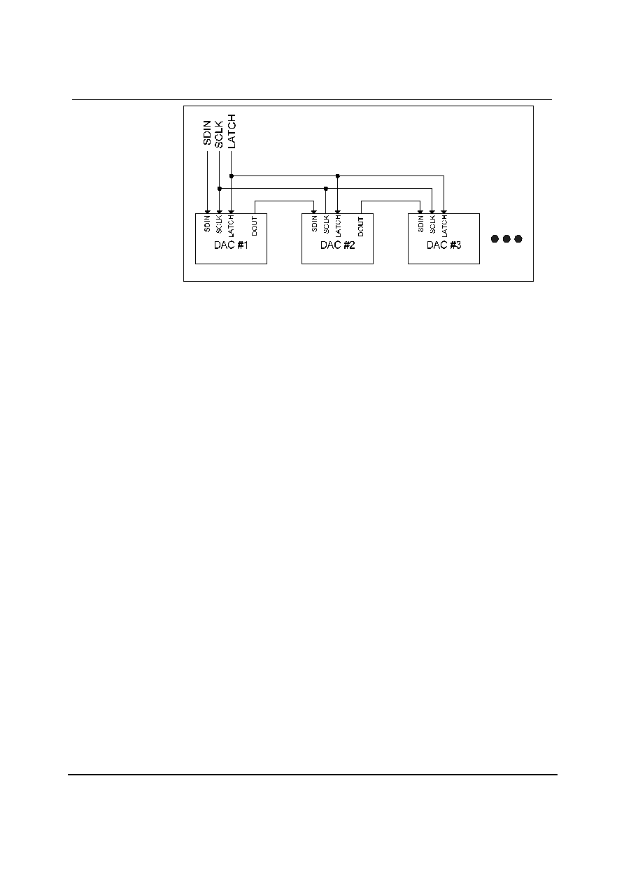
DAISY CHAINING MULTIPLE DEVICES
The DOUT pin 25 provides data sampled on DIN with a delay of 16 clock cycles. This signal can
be used to control another WM8719 or similar device in a daisy-chain type circuit. In this
configuration the LATCH signal should only go high once the correct number of SCLK's and
SDIN's to match the number of DAC in the daisy chain has been achieved. To write to a single
device in the chain a complete sequence needs to be written to all the devices with the ones that
are not to have any registry changes done to them to be feed an all 1 pattern.
WM8719
Preliminary Technical Data
w
PTD Rev 2.0 August 2003
18
Figure 16 Daisy Chain Scheme for Multiple Devices
WM8719
Preliminary Technical Data
w
PTD Rev 2.0 August 2003
19
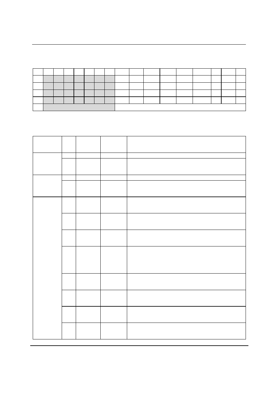
REGISTER MAP
WM8719 uses a total of 4 program registers, which are 16-bits long. These registers are all
loaded through input pin SDIN, using the 3-wire serial control mode as shown in Figure 7.
A6
A5
A4
A3
A2
A1
A0
D8
D7
D6
D5
D4
D3
D2
D1
D0
M0
0
0
0
0
0
0
0
UPDATEL
LAT7
LAT6
LAT5
LAT4
LAT3
LAT2
LAT1
LAT0
M1
0
0
0
0
0
0
1
UPDATER
RAT7
RAT6
RAT5
RAT4
RAT3
RAT2
RAT1
RAT0
M2
0
0
0
0
0
1
0
ZCDINIT ZEROFLR DSDMSLV DSDMODE DSDCLK[1]
DSDCLK[0] PWDN DEEMPH
MUT
M3
0
0
0
0
0
1
1
0
1
REV
BCP
ATC
LRP
FMT[1]
FMT[0]
IWL[1}
IWL[0]
ADDRESS
DATA
Table 2 Mapping of Program Registers
Note:
This register bit must be written as 0 otherwise device function can not be guaranteed
REGISTER
ADDRESS
(A3,A2,A1,A0)
BITS
NAME
DEFAULT
DESCRIPTION
[7:0]
LAT[7:0]
11111111 (0dB) Attenuation data for left channel in 0.5dB steps, see Table 5
0000
DACL
Attenuation
8
UPDATEL
0
Attenuation data load control for left channel.
0: Store DACL in intermediate latch (no change to output)
1: Store DACL and update attenuation on both channels.
[7:0]
RAT[7:0]
11111111 (0dB) Attenuation data for right channel in 0.5dB steps, see Table 5
0001
DACR
Attenuation
8
UPDATER
0
Attenuation data load control for right channel.
0: Store DACR in intermediate latch (no change to output)
1: Store DACR and update attenuation on both channels.
0
MUT
0
Left and right DACs soft mute control.
0: No mute
1: Mute
1
DEEMPH
0
De-emphasis control.
0: De-emphasis off
1: De-emphasis on
2
PWDN
0
Left and Right DACs Power-down Control
0: All DACs running, output is active
1: All DACs in power saving mode, output muted
4:3
DSDCLK
00
DSD master mode clock division:
00: DSDCLK128 = MCLK/2; DSDCLK64= MCLK/4
01: DSDCLK128 = MCLK/3; DSDCLK64= MCLK/6
10: DSDCLK128 = MCLK/4; DSDCLK64= MCLK/8
11: DSDCLK128 = MCLK/6; DSDCLK64= MCLK/12
5
DSDMODE
0
DSD/PCM mode select.
0: PCM mode
1: DSD mode
6
DSDMSLV
0
DSD mode master/slave selection.
0: Slave mode operation
1: Master mode operation
7
ZEROFLR
0
Zero flag pin control.
0: Channel independent
1: AND of both channels on ZEROFL output pin
0010
Mode Control
8
ZCDINIT
0
Zero cross detect Control.
0: Zero cross detect enabled
1: Zero cross detect disabled
WM8719
Preliminary Technical Data
w
PTD Rev 2.0 August 2003
20
REGISTER
ADDRESS
(A3,A2,A1,A0)
BITS
NAME
DEFAULT
DESCRIPTION
[1:0]
IWL[1:0]
10
Input Word Length.
00: 16-bit mode
01: 20-bit mode
10: 24-bit mode
11: 32-bit mode(not supported in right justified mode)
[3:2]
FMT[1:0]
10
Audio data format select.
00: right justified mode
01: left justified mode
10: I2S mode
11: DSP mode
4
LRP
0
Polarity select for LRCIN/DSP mode select.
0: normal LRCIN polarity/DSP late mode
1: inverted LRCIN polarity/DSP early mode
5
ATC
0
Attenuator Control.
0: All DACs use attenuation as programmed.
1: Right channel DACs use corresponding left DAC
attenuation
6
BCP
0
BCKIN, DSDCK64 Polarity
0: normal polarity
1: inverted polarity
0011
Format
Control
7
REV
0
Output phase reversal.
Table 3 Register Bit Descriptions
ATTENUATION CONTROL
Each DAC channel can be attenuated digitally before being applied to the digital filter.
Attenuation is 0dB by default but can be set between 0 and 127.5dB in 0.5dB steps using the 8
Attenuation control bits. All attenuation registers are double latched allowing new values to be
pre-latched to both channels before being updated synchronously. Setting the UPDATE bit on any
attenuation write will cause all pre-latched values to be immediately applied to the DAC channels.
REGISTER
ADDRESS
BITS
LABEL
DEFAULT
DESCRIPTION
[7:0]
LAT[7:0]
11111111 (0dB)
Attenuation data for Left channel DACL in 0.5dB steps.
0000
Attenuation
DACL
8
UPDATEL
0
Controls simultaneous update of all Attenuation Latches
0: Store DACL in intermediate latch (no change to output)
1: Store DACL and update attenuation on all channels.
[7:0]
RAT[7:0]
11111111 (0dB)
Attenuation data for Right channel DACR in 0.5dB steps.
0001
Attenuation
DACR
8
UPDATER
0
Controls simultaneous update of all Attenuation Latches
0: Store DACR in intermediate latch (no change to output)
1: Store DACR and update attenuation on all channels.
Table 4 Attenuation Register Map
Notes:
1.
The UPDATE bit is not latched. If UPDATE=0, the Attenuation value will be written to the pre-latch but not applied to the
relevant DAC. If UPDATE=1, all pre-latched values and the current value being written will be applied on the next input
sample.
2.
Care should be used in reducing the attenuation as rapid large volume changes can introduce zipper noise if the ZCDINIT
register bit has been set, (disabled).
WM8719
Preliminary Technical Data
w
PTD Rev 2.0 August 2003
21
DAC OUTPUT ATTENUATION
Registers DACR and DACL control the left and right channel attenuation. Table 9 shows how the
attenuation levels are selected from the 8-bit words.
DACX[7:0]
ATTENUATION LEVEL
00(hex)
dB (mute)
01(hex)
127.5dB
:
:
:
:
:
:
FE(hex)
0.5dB
FF(hex)
0dB
Table 5 Attenuation Control Levels
MUTE MODES
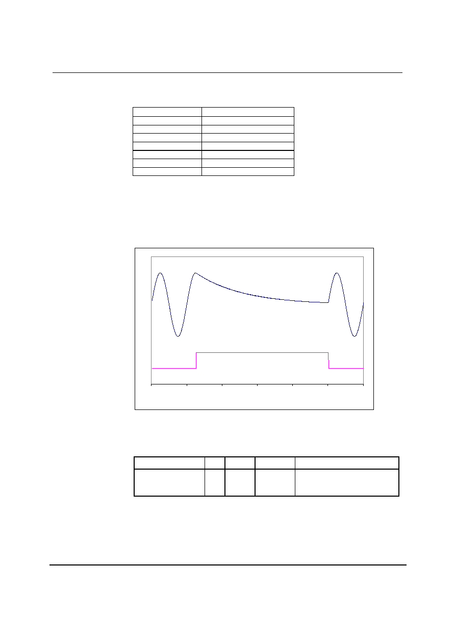
Figure 17 shows the application and release of MUTE whilst a full amplitude sinusoid is being
played at 48kHz sampling rate. When MUTE (lower trace) is asserted, the output (upper trace)
begins to decay exponentially from the DC level of the last input sample. The output will decay
towards V
MID
with a time constant of approximately 64 input samples. When MUTE is de-
asserted, the output will restart almost immediately from the current input sample.
-2.5
-2
-1.5
-1
-0.5
0
0.5
1
1.5
0
0.001
0.002
0.003
0.004
0.005
0.006
Time(s)
Figure 17 Application and Release of Soft Mute
Setting the MUT register bit will apply a 'soft' mute to the input of the digital filters:
REGISTER ADDRESS
BIT
LABEL
DEFAULT
DESCRIPTION
0010
Mode Control
0
MUT
0
Soft Mute select
0: Normal Operation
1: Soft mute both channels
WM8719
Preliminary Technical Data
w
PTD Rev 2.0 August 2003
22
DE-EMPHASIS MODE
Setting the DEEMPH register bit puts the digital filters into de-emphasis mode:
REGISTER ADDRESS
BIT
LABEL
DEFAULT
DESCRIPTION
0010
Mode Control
1
DEEMPH
0
De-emphasis mode select:
0: De-emphasis Off
1: De-emphasis On
POWERDOWN MODE
Setting the PWDN register bit immediately connects all outputs to V
MID
and selects a low power
mode. All trace of the previous input samples is removed, but all control register settings are
preserved. When PWDN is cleared in PCM mode again the first 16 input samples will be ignored,
as the FIR will repeat it's power-on initialisation sequence. The PWDN bit can also be used to
allow fast switching between PCM and DSD mode. By setting the PWDN bit during a mode
change the WM8719 will jump straight into the desired mode of operation, however this can
cause clicks on the output.
REGISTER ADDRESS
BIT
LABEL
DEFAULT
DESCRIPTION
0010
Mode Control
2
PWDN
0
Power Down Mode Select:
0: Normal Mode
1: Power Down Mode
DSD MASTER MODE CLOCK SELECT
The DSDCLISEL register bit controls the how the SCLK is divided to create the DSDCLK64 and
DSDCLK128 clocks, by selecting the appropriate input SCLK speed. 4 modes are supported.
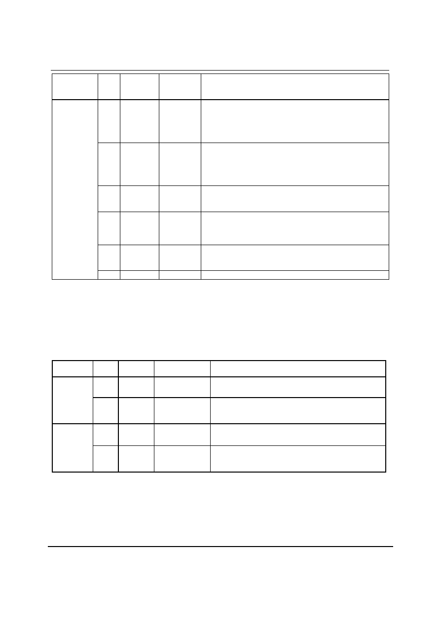
REGISTER ADDRESS
BIT
LABEL
DEFAULT
DESCRIPTION
0010
Mode Control
4:3
DSDCKISEL
00
DSD master mode clock division:
00: DSDCLK128 = MCLK/2;
DSDCLK64= MCLK/4
01: DSDCLK128 = MCLK/3;
DSDCLK64= MCLK/6
10: DSDCLK128 = MCLK/4;
DSDCLK64= MCLK/8
11: DSDCLK128 = MCLK/6;
DSDCLK64= MCLK/12
DSD MODE SELECTION
The DSDMODE register bit determines what mode the WM8719 is in. When in DSD mode only
bits 2, 3, 4, 5 and 7 of the Mode control register are used to control the chip, all other settings can
be changed but there effects will only take effect when the chip is put back into PCM mode.
REGISTER ADDRESS
BIT
LABEL
DEFAULT
DESCRIPTION
0010
Mode Control
5
DSDMODE
0
DSD/PCM mode select:
0: WM8719 is in PCM mode.
1: WM8719 is in DSD mode.
DSD MASTER SLAVE SELECTION
In DSD mode the DSDMLSV register bit controls whether the chip is working in DSD master
mode, (DSDCLK64, DSDCLk128 as an output), or in DSD slave mode, (DSDCLK64,
DSDCLK128 as an inputs). When in Master mode the selection of the DSDCKISEL bit determines
the division of MCLK need to create the 64fs and 128fs clocks. This register bit can be changed at
anytime however its effect will only take place on the next mode change from PCM to DSD.
WM8719
Preliminary Technical Data
w
PTD Rev 2.0 August 2003
23
REGISTER ADDRESS
BIT
LABEL
DEFAULT
DESCRIPTION
0010
Mode Control
6
DSDMSLV
0
DSD master/slave selection:
0: Slave mode.
1: Master mode.
ZERO FLAG OUTPUTS
The WM8719 has two zero flag outputs pins. The WM8719 asserts a low on the corresponding
zero flag pin when a sequence of more than 1024 midrail signal is inputted into the chip. The
user can use the zero flag pins to control external muting circuits if required. To simplify external
circuitry there is an option to have both zero flag output's ANDed internally and outputed on both
pins.
REGISTER
ADDRESS
BIT
LABEL
DEFAULT
DESCRIPTION
0010
Mode
Control
7
ZEROFLR
0
ZERO Flag outputs:
0: Both pins enabled.
1: AND of both channels to both pins.
ZERO CROSS DETECT
When the WM8719 receives updates to the volume levels it will, by default, wait for the signal to
pass through midrail for each channel before applying the update for that particular channel. This
ensures that there is minimum distortion seen on the output when the volume is changed.
REGISTER ADDRESS
BIT
LABEL
DEFAULT
DESCRIPTION
0010
Mode Control
8
ZCDINIT
0
Zero cross detect control:
0: Enabled
1: Disabled
SELECTION OF LRCIN POLARITY
In left justified, right justified or I
2
S modes, the LRP register bit controls the polarity of LRCIN. If
this bit is set high, the expected polarity of LRCIN will be the opposite of that shown in Figure 10,
Figure 11 and Figure 12. Note that if this feature is used as a means of swapping the left and right
channels, a 1 sample phase difference will be introduced.
REGISTER ADDRESS
BIT
LABEL
DEFAULT
DESCRIPTION
0011
Format Control
4
LRP
0
LRCIN Polarity (normal)
0: normal LRCIN polarity
1: inverted LRCIN polarity
In DSP modes, the LRCIN register bit is used to select between early and late modes (see Figure
13 and Figure 14.
REGISTER ADDRESS
BIT
LABEL
DEFAULT
DESCRIPTION
0011
Format Control
4
LRP
0
DSP Format (DSP modes)
0: Late DSP mode
1: Early DSP mode
In DSP early mode, the first bit is sampled on the BCKIN rising edge following the one that
detects a low to high transition on LRCIN. In DSP late mode, the first bit is sampled on the BCKIN
rising edge, which detects a low to high transition on LRCIN. No BCKIN edges are allowed
between the data words. The word order is DIN left, DIN right.
WM8719
Preliminary Technical Data
w
PTD Rev 2.0 August 2003
24
ATTENUATOR CONTROL MODE
Setting the ATC register bit causes the left channel attenuation settings to be applied to both left
and right channel DACs from the next audio input sample. No update to the attenuation registers
is required for ATC to take effect. (The right channels registry settings are preserved.)
REGISTER ADDRESS
BIT
LABEL
DEFAULT
DESCRIPTION
0011
PCM Control
5
ATC
0
Attenuator Control Mode:
0: Right channels use Right
attenuation
1: Right Channels use Left
Attenuation
BCKIN, DSDCLK64, DSDCLK128 POLARITY
By default in PCM mode, LRCIN and DIN are sampled on the rising edge of BCKIN and should
ideally change on the falling edge. Data sources which change LRCIN and DIN on the rising edge
of BCKIN can be supported by setting the BCP register bit. Setting BCP to 1 inverts the polarity
of BCKIN to the inverse of that shown in Figure 10, Figure 11, Figure 12, Figure 13 and Figure 14.
By default in DSD mode, DSDL and DSDR are sampled on the rising edge of DSCLK64, and a
multiple of the 64fs clock, 128fs, if operating in biphase mode, and should ideally changed on the
falling edge of DSDCLK64, or a multiple of the 64fs clock, 128fs, if in biphase mode. By using the
BCP registry bit the clocks can be reversed, so that the data is sampled on the falling edge.
REGISTER ADDRESS
BIT
LABEL
DEFAULT
DESCRIPTION
0011
PCM Control
6
BCP
0
BCKIN, DSDCLK64, DSDCLK128
0: normal polarity
1: inverted polarity
OUTPUT PHASE REVERSAL
The REV register bit controls the phase of the output signal. Setting the REV bit causes the
phase of the output signal to be inverted.
REGISTER ADDRESS
BIT
LABEL
DEFAULT
DESCRIPTION
0011
PCM Control
7
REV
0
Analogue Output Phase
0: Normal
1: Inverted
PCM DIGITAL AUDIO INTERFACE CONTROL REGISTERS
The WM8719 has a fully featured PCM digital audio interface whose interface format is selected
via the FMT [1:0] and IWL[1:0] register bits in register M3.
REGISTER ADDRESS
BIT
LABEL
DEFAULT
DESCRIPTION
0010
Format Control
1:0
IWL[1:0]
00
Interface format Select
0010
Format Control
3:2
FMT[1:0]
00
Interface format Select
WM8719
Preliminary Technical Data
w
PTD Rev 2.0 August 2003
25
FMT[1]
FMT[0]
IWL[1]
IWL[0]
AUDIO INTERFACE DESCRIPTION
(NOTE 1)
0
0
0
0
16 bit right justified mode
0
0
0
1
20 bit right justified mode
0
0
1
0
24 bit right justified mode
0
0
1
1
Not available
0
1
0
0
16 bit left justified mode
0
1
0
1
20 bit left justified mode
0
1
1
0
24 bit left justified mode
0
1
1
1
32 bit left justified mode
1
0
0
0
16 bit I
2
S mode
1
0
0
1
20 bit I
2
S mode
1
0
1
0
24 bit I
2
S mode
1
0
1
1
32 bit I
2
S mode
1
1
0
0
16 bit DSP mode
1
1
0
1
20 bit DSP mode
1
1
1
0
24 bit DSP mode
1
1
1
1
32 bit DSP mode
Table 6 Audio Data Input Format
Note:
In all modes, the data is signed 2's complement. The digital filters always input 24-bit data. If the
DAC is programmed to receive 16 or 20 bit data, the WM8719 pads the unused LSBs with
ZEROS. If the DAC is programmed into 32-bit mode, the 8 LSBs are treated as zero.
WM8719
Preliminary Technical Data
w
PTD Rev 2.0 August 2003
26
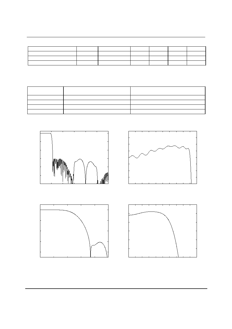
DIGITAL FILTER CHARACTERISTICS
PARAMETER
SYMBOL
TEST CONDITIONS
MIN
TYP
MAX
UNIT
Passband Edge
-3dB
0.487fs
Passband Ripple
f < 0.444fs
�
0.05
dB
Stopband Attenuation
f > 0.555fs
-60
dB
Table 7 Digital Filter Characteristics
SACD FILTER CHARACTERISTICS
With 64fs DSD data where fs = 44.1ks/s.
RESPONSE
FILTER RESPONSE WITHOUT POST-
FILTER
FILTER RESPONSE WITH 3
RD
ORDER
BUTTERWORTH POST-FILTER (-3DB AT 55KHZ)
Pass band peak ripple
0.017dB
0.017dB
Attenuation at 20kHz
-0.012dB
-0.021dB
Attenuation at 50kHz
-2.3dB
-3.9dB
Attenuation at 100kHz
-15.5dB
-31dB
Table 8 Overall Frequency Response in SCAD Mode
DAC FILTER RESPONSES
-120
-100
-80
-60
-40
-20
0
0
0.5
1
1.5
2
2.5
3
Response (dB)
Frequency (Fs)
Figure 18 DAC Digital Filter Frequency Response
-44.1, 48 and 96kHz
-0.2
-0.15
-0.1
-0.05
0
0.05
0.1
0.15
0.2
0
0.05
0.1
0.15
0.2
0.25
0.3
0.35
0.4
0.45
0.5
Response (dB)
Frequency (Fs)
Figure 19 DAC Digital Filter Ripple
-44.1, 48 and 96kHz
-80
-60
-40
-20
0
0
0.2
0.4
0.6
0.8
1
Response (dB)
Frequency (Fs)
Figure 20 DAC Digital Filter Frequency Response
-192kHz
-1
-0.8
-0.6
-0.4
-0.2
0
0.2
0
0.05
0.1
0.15
0.2
0.25
0.3
0.35
0.4
0.45
0.5
Response (dB)
Frequency (Fs)
Figure 21 DAC Digital Filter Ripple
-192kHz
WM8719
Preliminary Technical Data
w
PTD Rev 2.0 August 2003
27
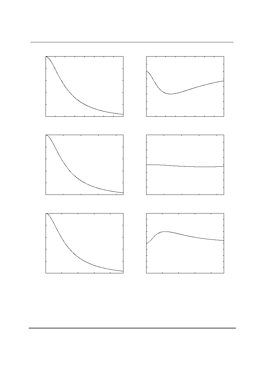
DIGITAL DE-EMPHASIS CHARACTERISTICS
-10
-8
-6
-4
-2
0
0
2
4
6
8
10
12
14
16
Response (dB)
Frequency (kHz)
Figure 22 De-Emphasis Frequency Response (32kHz)
-3
-2.5
-2
-1.5
-1
-0.5
0
0.5
1
0
2
4
6
8
10
12
14
16
Response (dB)
Frequency (kHz)
Figure 23 De-Emphasis Error (32kHz)
-10
-8
-6
-4
-2
0
0
5
10
15
20
Response (dB)
Frequency (kHz)
Figure 24 De-Emphasis Frequency Response (44.1kHz)
-0.4
-0.3
-0.2
-0.1
0
0.1
0.2
0.3
0.4
0
5
10
15
20
Response (dB)
Frequency (kHz)
Figure 25 De-Emphasis Error (44.1kHz)
-10
-8
-6
-4
-2
0
0
5
10
15
20
Response (dB)
Frequency (kHz)
Figure 26 De-Emphasis Frequency Response (48kHz)
-1
-0.8
-0.6
-0.4
-0.2
0
0.2
0.4
0.6
0.8
1
0
5
10
15
20
Response (dB)
Frequency (kHz)
Figure 27 De-Emphasis Error (48kHz)

WM8719
Preliminary Technical Data
w
PTD Rev 2.0 August 2003
28
DSD MODE CHARACTERISTICS
The following filter responses show the DAC output frequency response in SACD or DSD mode, with and without an external 3
rd
order Lowpass filter. Table 8 gives details of the attenuation versus frequency of the two cases.
-0.25
-0.2
-0.15
-0.1
-0.05
0
0.05
0
5000
10000
15000
20000
25000
Gain (dB)
Frequency (Hz)
Chip output
Output and 3rd order Butterworth filter
Figure 28 DSD Mode Frequency Response � to 25kHz
-10
-8
-6
-4
-2
0
0
10000
20000
30000
40000
50000
60000
Gain (dB)
Frequency (Hz)
Chip output
Output and 3rd order Butterworth filter
Figure 29 DSD Mode Frequency Response � to 60kHz
-50
-40
-30
-20
-10
0
10
0
20000
40000
60000
80000
100000
120000
Gain (dB)
Frequency (Hz)
Chip output
Output and 3rd order Butterworth filter
Figure 30 DSD Mode Frequency Response - to 120kHz
-140
-120
-100
-80
-60
-40
-20
0
20
0
200000
400000
600000
800000
1e+06
Gain (dB)
Frequency (Hz)
Chip output
Output and 3rd order Butterworth filter
Figure 31 DSD Mode Frequency Response � to 1MHz

WM8719
Preliminary Technical Data
w
PTD Rev 2.0 August 2003
29
TYPICAL PERFORMANCE
Figure 32 THD+N versus Input Amplitude (@ 1kHz, 'A' weighted)
Figure 33 THD+N versus Frequency (@ 1kHz, 'A' weighted)
WM8719
Preliminary Technical Data
w
PTD Rev 2.0 August 2003
30
APPLICATIONS INFORMATION
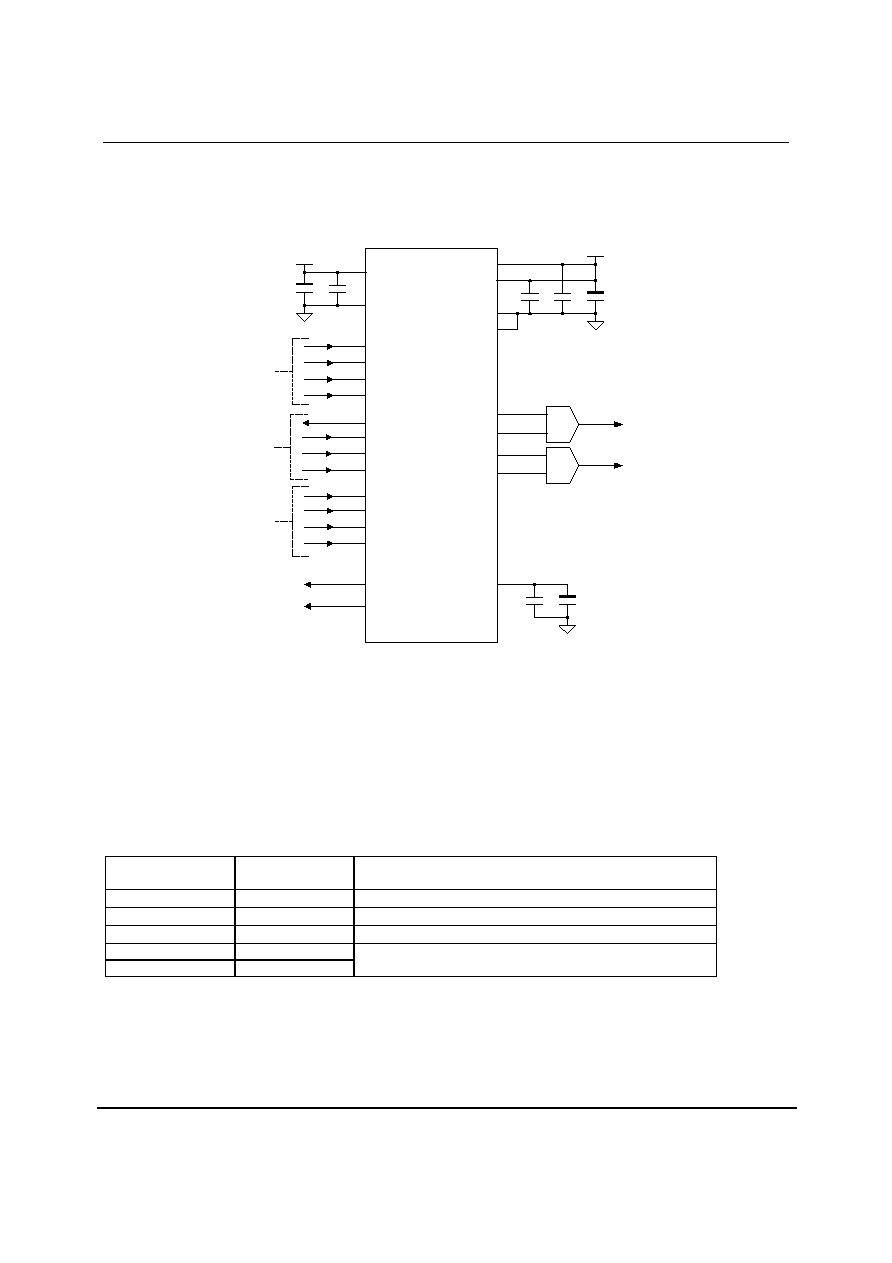
RECOMMENDED EXTERNAL COMPONENTS (PCM/DSD SLAVE MODE)
2
LATCH
AGND
AVDD
VMID
C
7
C
6
GND
25
21
Software I/F Control
WM8719
C
4
C
5
3
SCLK
4
SDIN
AVDD
26
MCLK
27
BCKIN
28
DIN
PCM Audio Serial Data I/F
AGND
1
LRCIN
7
10
+
11
+
12
ZEROFR
17
ZEROFL
VOUTRN
VOUTRP
-
-
+
+
13
14
LEFT AUDIO
OUTPUT
RIGHT AUDIO
OUTPUT
VOUTLP
15
VOUTLN
16
22
20
DSD Audio Serial Data I/F
SDOUT
DSDCLK64
DSDL
DSDR
VREFP
8
VREFN
9
C
3
DVDD
DGND
5
6
+
C
1
C
2
23
DSDCLK128
NOTES:
1. AGND and DGND should be connected as close to the WM8719 as possible.
2. C
1
, C
2
, C
5
and C
6
should be positioned as close to the WM8719 as possible.
3. Capacitor types should be carefully chosen. Capacitors with very low ESR are
recommended for optimum performance.
DVDD
DGND
Figure 34 External Components Diagram � Slave Mode
RECOMMENDED EXTERNAL COMPONENTS VALUES
COMPONENT
REFERENCE
SUGGESTED
VALUE
DESCRIPTION
C1 and C5
10
�
F
De-coupling for DVDD and AVDD
C2 and C4
0.1
�
F
De-coupling for DVDD and AVDD
C3
0.1uF
De-coupling for VREFP positive DAC reference supply
C6
0.1
�
F
C7
10
�
F
Reference de-coupling capacitors for VMID pin.
Table 9 External Components Description
WM8719
Preliminary Technical Data
w
PTD Rev 2.0 August 2003
31
RECOMMENDED EXTERNAL COMPONENTS (PCM/DSD MASTER MODE)
2
LATCH
AGND
AVDD
VMID
C
7
C
6
GND
25
21
Software I/F Control
WM8719
C
4
C
5
3
SCLK
4
SDIN
AVDD
26
MCLK
27
BCKIN
28
DIN
PCM Audio Serial Data I/F
AGND
1
LRCIN
7
10
+
11
+
12
ZEROFR
17
ZEROFL
VOUTRN
VOUTRP
-
-
+
+
13
14
LEFT AUDIO
OUTPUT
RIGHT AUDIO
OUTPUT
VOUTLP
15
VOUTLN
16
22
20
DSD Audio Serial Data I/F
SDOUT
DSDCLK64
DSDL
DSDR
VREFP
8
VREFN
9
C
3
DVDD
DGND
5
6
+
C
1
C
2
23
DSDCLK128
NOTES:
1. AGND and DGND should be connected as close to the WM8719 as possible.
2. C
1
, C
2
, C
5
and C
6
should be positioned as close to the WM8719 as possible.
3. Capacitor types should be carefully chosen. Capacitors with very low ESR are
recommended for optimum performance.
DGND
DVDD
Figure 35 External Components Diagram � Master Mode
RECOMMENDED EXTERNAL COMPONENTS VALUES
COMPONENT
REFERENCE
SUGGESTED
VALUE
DESCRIPTION
C1 and C5
10
�
F
De-coupling for DVDD and AVDD
C2 and C4
0.1
�
F
De-coupling for DVDD and AVDD
C3
0.1uF
De-coupling for VREFP positive DAC reference supply
C6
0.1
�
F
C7
10
�
F
Reference de-coupling capacitors for VMID pin.
WM8719
Preliminary Technical Data
w
PTD Rev 2.0 August 2003
32
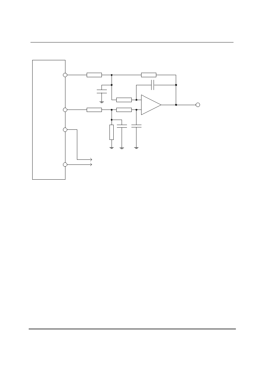
RECOMMENDED ANALOGUE LOW PASS FILTER FOR PCM DATA FORMAT
(OPTIONAL)
WM8719
LOUTN
LOUTP
R1 2K7
R2 2K7
R3 3K
R5
R4
R6
2K7
2K7
3K
C1
680pF
C2
220pF
C3
680pF
C4
220pF
-
+
OP
Left
ROUTN
ROUTP
other
channel
Right
Figure 36 Recommended Low Pass Filter (Optional)
WM8719
Preliminary Technical Data
w
PTD Rev 2.0 August 2003
33
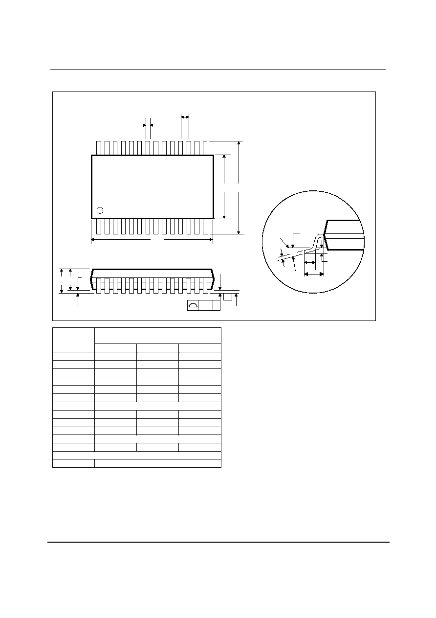
PACKAGE DIMENSIONS
NOTES:
A. ALL LINEAR DIMENSIONS ARE IN MILLIMETERS.
B. THIS DRAWING IS SUBJECT TO CHANGE WITHOUT NOTICE.
C. BODY DIMENSIONS DO NOT INCLUDE MOLD FLASH OR PROTRUSION, NOT TO EXCEED 0.20MM.
D. MEETS JEDEC.95 MO-150, VARIATION = AH. REFER TO THIS SPECIFICATION FOR FURTHER DETAILS.
DM007.D
DS: 28 PIN SSOP (10.2 x 5.3 x 1.75 mm)
Symbols
Dimensions
(mm)
MINN
OM
MAX
A
-----
-----
2.0
A
1
0.05
-----
0.25
A
2
1.65
1.75
1.85
b
0.22
0.30
0.38
c
0.09
-----
0.25
D
9.90
10.20
10.50
e
E
7.40
7.80
8.20
5.00
5.30
5.60
L
0.55
0.75
0.95
A A2
A1
14
1
15
28
E1
E
c
L
GAUGE
PLANE
0.25
e
b
D
SEATING PLANE
-C-
0.10 C
REF:
JEDEC.95, MO-150
E
1
L
1
0.125 REF
0.65 BSC
L
1
0
o
4
o
8
o

WM8719
Preliminary Technical Data
w
PTD Rev 2.0 August 2003
34
IMPORTANT NOTICE
Wolfson Microelectronics plc (WM) reserve the right to make changes to their products or to discontinue any product or service
without notice, and advise customers to obtain the latest version of relevant information to verify, before placing orders, that
information being relied on is current. All products are sold subject to the WM terms and conditions of sale supplied at the time
of order acknowledgement, including those pertaining to warranty, patent infringement, and limitation of liability.
WM warrants performance of its products to the specifications applicable at the time of sale in accordance with WM's standard
warranty. Testing and other quality control techniques are utilised to the extent WM deems necessary to support this warranty.
Specific testing of all parameters of each device is not necessarily performed, except those mandated by government
requirements.
In order to minimise risks associated with customer applications, adequate design and operating safeguards must be used by
the customer to minimise inherent or procedural hazards. Wolfson products are not authorised for use as critical components in
life support devices or systems without the express written approval of an officer of the company. Life support devices or
systems are devices or systems that are intended for surgical implant into the body, or support or sustain life, and whose failure
to perform when properly used in accordance with instructions for use provided, can be reasonably expected to result in a
significant injury to the user. A critical component is any component of a life support device or system whose failure to perform
can be reasonably expected to cause the failure of the life support device or system, or to affect its safety or effectiveness.
WM assumes no liability for applications assistance or customer product design. WM does not warrant or represent that any
license, either express or implied, is granted under any patent right, copyright, mask work right, or other intellectual property
right of WM covering or relating to any combination, machine, or process in which such products or services might be or are
used. WM's publication of information regarding any third party's products or services does not constitute WM's approval,
license, warranty or endorsement thereof.
Reproduction of information from the WM web site or datasheets is permissible only if reproduction is without alteration and is
accompanied by all associated warranties, conditions, limitations and notices. Representation or reproduction of this information
with alteration voids all warranties provided for an associated WM product or service, is an unfair and deceptive business
practice, and WM is not responsible nor liable for any such use.
Resale of WM's products or services with statements different from or beyond the parameters stated by WM for that product or
service voids all express and any implied warranties for the associated WM product or service, is an unfair and deceptive
business practice, and WM is not responsible nor liable for any such use.
ADDRESS:
Wolfson Microelectronics plc
20 Bernard Terrace
Edinburgh
EH8 9NX
United Kingdom
Tel :: +44 (0)131 272 7000
Fax :: +44 (0)131 272 7001
Email ::
sales@wolfsonmicro.com