Document Outline
- WM8720
- 24-bit, 96kHz Stereo DAC with Volume Control
- Production Data, November 2000, Rev 3.0
- DESCRIPTION
- FEATURES
- APPLICATIONS
- BLOCK DIAGRAM
- PIN CONFIGURATION
- ORDERING INFORMATION
- PIN DESCRIPTION
- ABSOLUTE MAXIMUM RATINGS
- RECOMMENDED OPERATING CONDITIONS
- ELECTRICAL CHARACTERISTICS
- DEVICE DESCRIPTION
- SYSTEM CLOCK
- AUDIO DATA INTERFACE
- MODES OF OPERATION
- HARDWARE CONTROL MODES
- SOFTWARE CONTROL INTERFACE
- REGISTER MAP
- RECOMMENDED EXTERNAL COMPONENTS
- RECOMMENDED EXTERNAL COMPONENTS VALUES
- PACKAGE DIMENSIONS
WM8720
24-bit, 96kHz Stereo DAC with Volume Control
Production Data, November 2000, Rev 3.0
WOLFSON MICROELECTRONICS LTD
Lutton Court, Bernard Terrace, Edinburgh, EH8 9NX, UK
Tel: +44 (0) 131 667 9386
Fax: +44 (0) 131 667 5176
Email: sales@wolfson.co.uk
http://www.wolfson.co.uk
Production Data Datasheets contain final
specifications current on publication date.
Supply of products conforms to Wolfson
Microelectronics' Terms and Conditions.
2000 Wolfson Microelectronics Ltd
.
DESCRIPTION
The WM8720 is a high performance stereo DAC designed
for audio applications such as CD, DVD, home theatre
systems, set top boxes and digital TV. The WM8720
supports data input word lengths from 16 to 24-bits and
sampling rates up to 96kHz. The WM8720 consists of a
serial interface port, digital interpolation filter, multi-bit
sigma delta modulator and stereo DAC in a small 20-pin
SSOP package. The WM8720 also includes a digitally
controllable mute and attenuator function on each channel.
The WM8720 supports a variety of connection schemes for
audio DAC control. The SPI-compatible serial control port
provides access to a wide range of features including on-
chip mute, attenuation and phase reversal. A hardware
controllable interface is also available.
The programmable data input port supports a variety of
glueless interfaces to popular DSPs, audio decoders and
S/PDIF and AES/EBU receivers.
FEATURES
�
Performance:
-
102dB SNR (`A' weighted @48kHz),
-
THD: -95dB @ 0dB FS
�
5V or 3.3V supply operation
�
Sampling frequency: 8kHz to 96kHz
�
Input data word: 16 to 24-bit
�
Hardware or SPI compatible serial port control modes:
-
Hardware mode: system clock, reset, mute,
de-emphasis
-
Serial control mode: mute, de-emphasis, digital
attenuation (256 steps), zero mute, phase reversal,
power down
�
Compatible with PCM1720
APPLICATIONS
�
CD, DVD audio
�
Home theatre systems
�
Set top boxes
�
Digital
TV
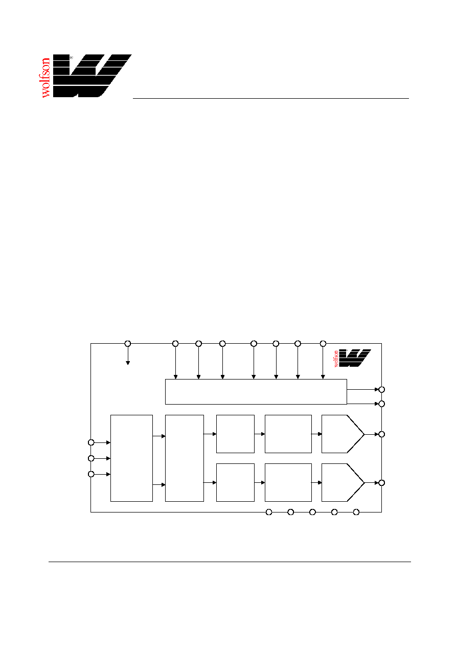
BLOCK DIAGRAM
SERIAL
INTERFACE
DIGITAL
FILTERS
CONTROL INTERFACE
BCKIN (14)
(9) VOUTR
(12) VOUTL
SIGMA
DELTA
MODULATOR
MUTE/
ATTEN
(20)
DGND
(10)
AGND
(13)
CAP
(11)
AVDD
(19)
DVDD
LRCIN (16)
DIN (15)
(3) TEST
(8) ZERO
256fs/384fs
MUTE
(17)
MODE
(18)
RSTB
(7)
PWDN
(1)
MD/DM
(6)
MC/IWL
(5)
ML/I2S
(4)
SCKI
(2)
DAC
SIGMA
DELTA
MODULATOR
MUTE/
ATTEN
DAC
WM8720
WM8720
Production Data
WOLFSON MICROELECTRONICS LTD
PD Rev 3.0 November 2000
2
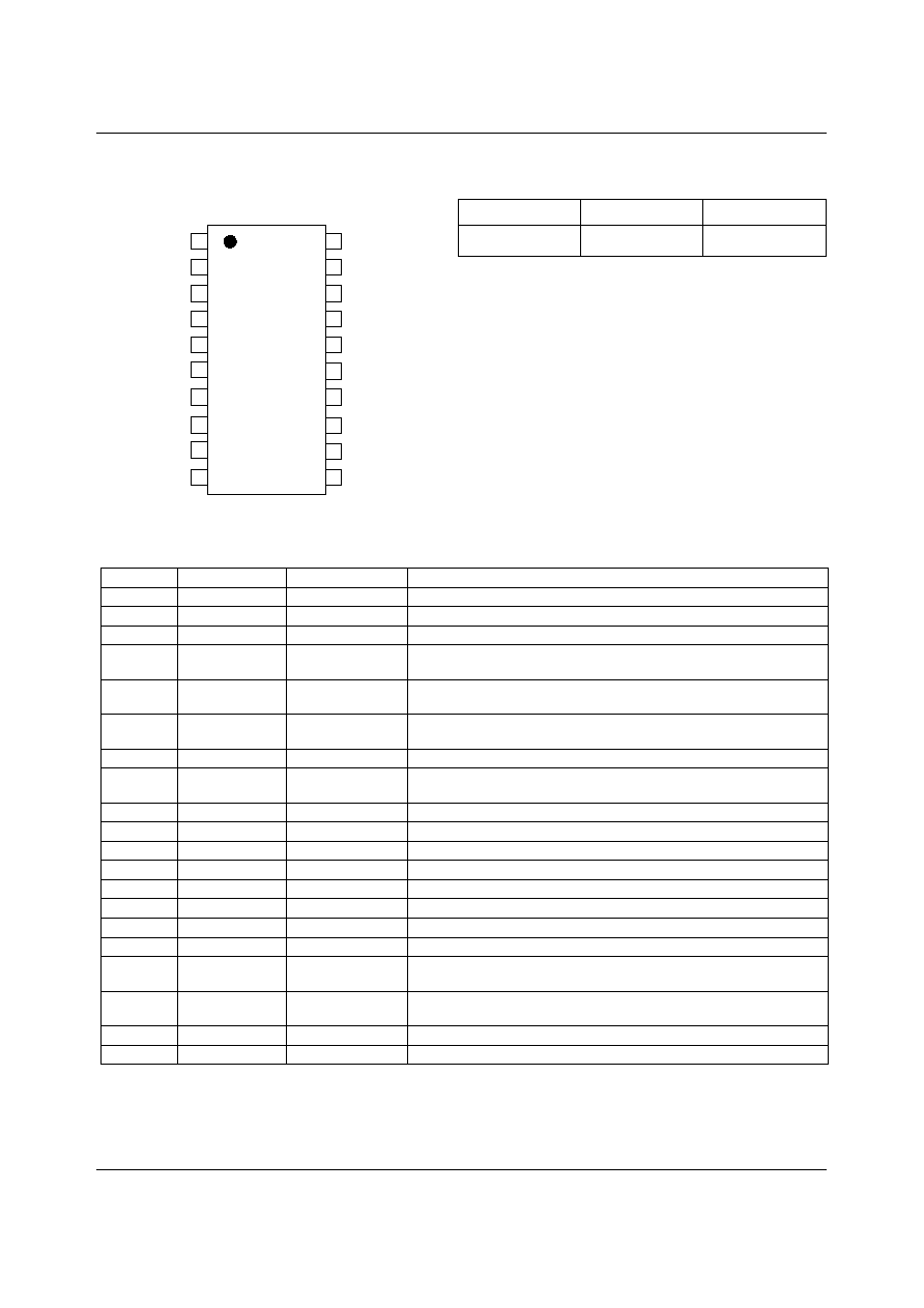
PIN CONFIGURATION
ORDERING INFORMATION
DEVICE
TEMP. RANGE
PACKAGE
WM8720EDS
-25 to +85
o
C
20-pin SSOP
16
15
14
20
19
18
17
5
6
7
1
2
3
4
BCKIN
DIN
LRCIN
MUTE
MODE
DGND
DVDD
RSTB
MD/DM
MC/IWL
ML/I2S
TEST
PWDN
SCKI
13
12
11
8
9
10
AVDD
VOUTL
CAP
AGND
VOUTR
ZERO
PIN DESCRIPTION
PIN
NAME
TYPE
DESCRIPTION
1
PWDN
Digital input
Powerdown control; low is ON, high is POWER OFF. Internal pull-down.
2
SCKI
Digital input
System clock input (256 or 384fs).
3
TEST
Digital output
Reserved.
4
ML/I2S
Digital input
Latch enable (software mode) or input format selection (hardware mode).
Internal pull-up.
5
MC/IWL
Digital input
Serial control data clock input (software mode) or input word length
selection (hardware mode). Internal pull-up.
6
MD/DM
Digital input
Serial control data input (software mode) or de-emphasis selection
(hardware mode). Internal pull-up.
7
RSTB
Digital input
Reset input � active low. Internal pull-up.
8
ZERO
Digital output
Infinite zero detect � active low. Open drain type output with active
pull-down.
9
VOUTR
Analogue output
Right channel DAC output.
10
AGND
Supply
Analogue ground supply.
11
AVDD
Supply
Analogue positive supply.
12
VOUTL
Analogue output
Left channel DAC output.
13
CAP
Analogue output
Analogue internal reference.
14
BCKIN
Digital input
Audio data bit clock input.
15
DIN
Digital input
Serial audio data input.
16
LRCIN
Digital input
Sample rate clock input.
17
MUTE
Digital IO
Mute control pin, input or automute output.
Low is not mute, high is mute, Z is automute.
18
MODE
Digital input
Mode select pin. Low is software mode, high is hardware control.
Internal pull-down.
19
DVDD
Supply
Digital positive supply.
20
DGND
Supply
Digital ground supply.
Note:
Digital input pins have Schmitt trigger input buffers.

Production Data
WM8720
WOLFSON MICROELECTRONICS LTD
PD Rev 3.0 November 2000
3
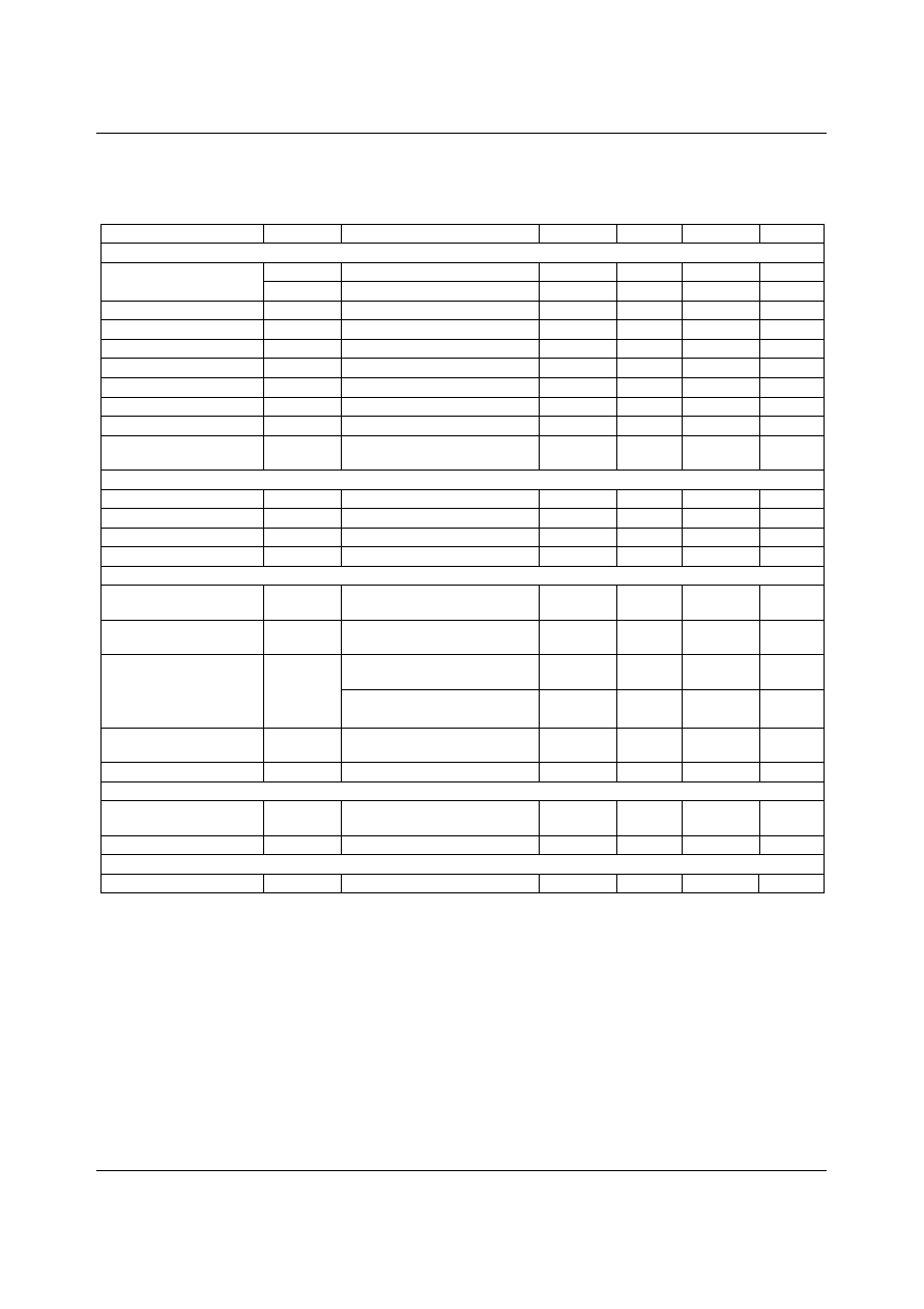
ABSOLUTE MAXIMUM RATINGS
Absolute Maximum Ratings are stress ratings only. Permanent damage to the device may be caused by continuously operating at
or beyond these limits. Device functional operating limits and guaranteed performance specifications are given under Electrical
Characteristics at the test conditions specified.
ESD Sensitive Device. This device is manufactured on a CMOS process. It is therefore generically susceptible
to damage from excessive static voltages. Proper ESD precautions must be taken during handling and storage
of this device.
CONDITION
MIN
MAX
Supply voltage
-0.3V
+7V
Reference input
VDD + 0.3V
Operating temperature range, T
A
-25
o
C
+85
o
C
Storage temperature
-65
o
C
+150
o
C
Package body temperature (soldering, 10 seconds)
+240
o
C
Package body temperature (soldering, 2 minutes)
+183
o
C
RECOMMENDED OPERATING CONDITIONS
PARAMETER
SYMBOL
TEST CONDITIONS
MIN
TYP
MAX
UNIT
Digital supply range
DVDD
-10%
3.3 to 5
+10%
V
Analogue supply range
AVDD
-10%
3.3 to 5
+10%
V
Ground
AGND, DGND
0
V
Difference DGND to AGND
-0.3
0
+0.3
V
Analogue supply current
AVDD = 5V
17
mA
Digital supply current
DVDD = 5V
6
mA
Analogue supply current
AVDD = 3.3V
16
mA
Digital supply current
DVDD = 3.3V
3
mA
Standby analogue current
AVDD = 5V
1.7
mA
Standby digital current
DVDD = 5V
30
�
A
WM8720
Production Data
WOLFSON MICROELECTRONICS LTD
PD Rev 3.0 November 2000
4
ELECTRICAL CHARACTERISTICS
Test Conditions
AVDD, DVDD = 5V, AGND, DGND = 0V, T
A
= +25
o
C, fs = 48kHz, SCKI = 256fs unless otherwise stated.
PARAMETER
SYMBOL
TEST CONDITIONS
MIN
TYP
MAX
UNIT
DAC Circuit Specifications
SNR (Note 1)
AVDD, DVDD = 5V
95
102
dB
AVDD, DVDD = 3.3V
100
dB
THD
0dB FS
-96
-85
dB
Dynamic range
THD+N @ -60dB FS
95
102
dB
Passband
�
0.25dB
0.4535
fs
Stopband
-3dB
0.491
fs
Pass band ripple
�0.25
dB
Out of band rejection
-40
dB
Channel Separation
98
dB
Gain mismatch
channel-to-channel
0dB FS
�0.5
�5
%FSR
Digital Logic Levels
Input LOW level
V
IL
0.8
V
Input HIGH level
V
IH
2.0
V
Output LOW level
V
OL
I
OL
= 2mA
AV
SS
+ 0.3V
Output HIGH level
V
OH
I
OH
= 2mA
AVDD
- 0.3V
Analogue Output Levels
Output level
Into 10kohm, full scale 0dB,
(5V supply)
1.1
V
RMS
Into 10kohm, full scale 0dB,
(3.3V supply)
0.72
V
RMS
To midrail or AC coupled
(5V supply)
1
kohms
Minimum resistance load
To midrail or AC coupled
(3.3V supply)
1
kohms
Maximum capacitance
load
5V or 3.3V
100
pF
Output DC level
AVDD/2
V
Reference Levels
Potential divider
resistance
AVDD to CAP and CAP to AGND
90
kohms
Voltage at CAP
AVDD/2
POR
POR threshold
2.0
V
TERMINOLOGY
1.
Signal-to-noise ratio (dB) (SNR) is a measure of the difference in level between the full-scale output and the output
with no signal applied.
2.
Dynamic range (dB) (DNR) is a measure of the difference between the highest and lowest portions of a signal.
Normally a THD+N measurement at 60dB below full scale. The measured signal is then corrected by adding the 60dB
to it. (eg THD+N @ -60dB= -32dB, DR= 92dB).
3.
THD+N (dB) is a ratio of the r.m.s. values, of (Noise + Distortion)/Signal.
4.
Stop band attenuation (dB) is the degree to which the frequency spectrum is attenuated (outside audio band).
5.
Channel Separation (dB) (also known as Cross-Talk) is a measure of the amount one channel is isolated from the
other. Normally measured by sending a full-scale signal down one channel and measuring the other.
6.
Pass-Band Ripple - Any variation of the frequency response in the pass-band region.
Production Data
WM8720
WOLFSON MICROELECTRONICS LTD
PD Rev 3.0 November 2000
5
BCKIN
DIN
LRCIN
t
BCH
t
BCL
t
BL
t
LB
t
BCY
t
DS
t
DH
Figure 1 Audio Data Input Timing
Test Conditions
AVDD, DVDD = 5V, AGND, DGND = 0V, T
A
= +25
o
C, fs = 48kHz, SCKI = 256fs unless otherwise stated.
PARAMETER
SYMBOL
TEST CONDITIONS
MIN
TYP
MAX
UNIT
Audio Data Input Timing Information
BCKIN pulse cycle time
t
BCY
100
ns
BCKIN pulse width high
t
BCH
40
ns
BCKIN pulse width low
t
BCL
40
ns
BCKIN rising edge to
LRCIN edge
t
BL
20
ns
LRCIN rising edge to
BCKIN rising edge
t
LB
20
ns
DIN setup time
t
DS
20
ns
DIN hold time
t
DH
20
ns
SCKI
t
SCKIL
t
SCKIH
t
SCKY
Figure 2 System Clock Timing Requirements
Test Conditions
AVDD, DVDD = 5V, AGND, DGND = 0V, T
A
= +25
o
C, fs = 48kHz, SCKI = 256fs unless otherwise stated.
PARAMETER
SYMBOL
TEST CONDITIONS
MIN
TYP
MAX
UNIT
System Clock Timing Information
System clock pulse width high
t
SCKIH
10
ns
System clock pulse width low
t
SCKIL
10
ns
System clock cycle time
t
SCKY
27
ns