Document Outline
- WM8729
- 24-bit, 192kHz Stereo DAC
- Product Preview, Rev 1.2, April 2001
- DESCRIPTION
- FEATURES
- APPLICATIONS
- BLOCK DIAGRAM
- PIN CONFIGURATION
- ORDERING INFORMATION
- PIN DESCRIPTION
- ABSOLUTE MAXIMUM RATINGS
- DC ELECTRICAL CHARACTERISTICS
- ELECTRICAL CHARACTERISTICS
- DEVICE DESCRIPTION
- INTRODUCTION
- CLOCKING SCHEMES
- DIGITAL AUDIO INTERFACE
- AUDIO DATA SAMPLING RATES
- HARDWARE CONTROL MODES
- DIGITAL FILTER CHARACTERISTICS
- DIGITAL DE-EMPHASIS CHARACTERISTICS
- PACKAGE DRAWING
- RECOMMENDED EXTERNAL COMPONENTS
- RECOMMENDED EXTERNAL COMPONENTS VALUES
- RECOMMENDED ANALOGUE LOW PASS FILTER (OPTIONAL)

WM8729
24-bit, 192kHz Stereo DAC
Product Preview, Rev 1.2, April 2001
WOLFSON MICROELECTRONICS LTD
Lutton Court, Bernard Terrace, Edinburgh, EH8 9NX, UK
Tel: +44 (0) 131 667 9386
Fax: +44 (0) 131 667 5176
Email: sales@wolfson.co.uk
www.wolfsonmicro.com
Product Preview data sheets contain
specifications for products in the formative
phase of development. These products may
be changed or discontinued without notice.
2001 Wolfson Microelectronics Ltd
.
DESCRIPTION
The WM8729 is a high performance stereo DAC designed
for audio applications such as DVD, home theatre systems,
and digital TV. The WM8729 supports data input word
lengths from 16 to 24-bits and sampling rates up to 192kHz.
The WM8729 consists of a serial interface port, digital
interpolation filters, multi-bit sigma delta modulators and
stereo DAC in a small 16-pin SOIC package.
The WM8729 has a hardware control interface for selection
of audio data interface format and de-emphasis.
The WM8729 is an ideal device to interface to AC-3
,
DTS
, and MPEG audio decoders for surround sound
applications, or for use in DVD players, including supporting
the implementation of 2 channels at 192kHz for high-end
DVD-Audio applications.
FEATURES
�
Stereo
DAC
�
Audio
Performance
-
106dB SNR (`A' weighted @ 48kHz) DAC
-
-97dB
THD
�
DAC Sampling Frequency: 8kHz � 192kHz
�
Pin Selectable Audio Data Interface Format
-
I
2
S or Right Justified
�
3.0V - 5.5V Supply Operation
�
16-pin SOIC Package
�
Exceeds Dolby Class A Performance Requirements
APPLICATIONS
�
DVD-Audio and DVD `Universal' Players
�
Home theatre systems
�
Digital
TV
�
Digital broadcast receivers
BLOCK DIAGRAM
SERIAL
INTERFACE
MUTE
CONTROL INTERFACE
BCKIN
VOUTL
VOUTR
SIGMA
DELTA
MODULATOR
LRCIN
DIN
MUTE
SIGMA
DELTA
MODULATOR
DIGITAL FILTERS
MCLK
DVDD
AVDD
AGND
DGND
DEM
MUTEB
FORMAT
LOW
PASS
FILTER
LOW
PASS
FILTER
VMID
RIGHT
DAC
LEFT
DAC
VREFN
VREFP
WM8729
WM8729
Product Preview
WOLFSON MICROELECTRONICS LTD
PP Rev 1.2 April 2001
2
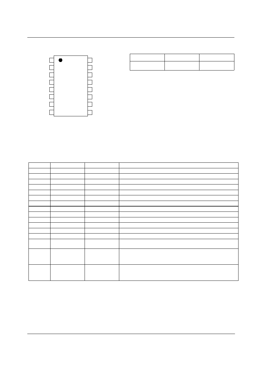
PIN CONFIGURATION
ORDERING INFORMATION
DEVICE
TEMP. RANGE
PACKAGE
XWM8729ED
-25 to +85
o
C
16-pin SOIC
VOUTL
VMID
VREFN
VREFP
MUTEB
FORMAT
DEM
DVDD
BCKIN
LRCIN
AVDD
WM8729
12
11
10
16
15
14
13
5
6
7
1
2
3
4
VOUTR
DGND
MCLK
DIN
9
8
AGND
PIN DESCRIPTION
PIN
NAME
TYPE
DESCRIPTION
1
LRCIN
Digital Input
DAC Sample Rate Clock Input
2
DIN
Digital Input
Serial Audio Data Input
3
BCKIN
Digital Input
Audio Data Bit Clock Input.
4
MCLK
Analogue Input
Master Clock Input
5
DGND
Supply
Digital Ground Supply
6
DVDD
Supply
Digital Positive Supply
7
VOUTR
Analogue Output
Right Channel DAC Output
8
AGND
Supply
Analogue Ground Supply
9
AVDD
Supply
Analogue Positive Supply
10
VOUTL
Analogue Output
Left Channel DAC Output
11
VMID
Analogue Output
Mid Rail Decoupling Point
12
VREFN
Supply
DAC Negative Reference � normally AGND, must not be below AGND
13
VREFP
Supply
DAC Positive Reference � normally AVDD, must not be above AVDD
14
MUTEB
Digital Bi-directional
Mute Control, (L = Mute on, H = Mute off, Z = Automute Enabled)
15
DEM
Digital Input
De-Emphasis Select
0 = De-Emphasis Off
1 = De-Emphasis On
16
FORMAT
Digital Input
(Pull-Up)
Digital Audio Data Input Format Selection
0 = Right justified Audio Data
1 = I
2
S Audio Data
Note:
Digital input pins have Schmitt trigger input buffers.

WM8729
Product Preview
WOLFSON MICROELECTRONICS LTD
PP Rev 1.2 April 2001
3
ABSOLUTE MAXIMUM RATINGS
Absolute Maximum Ratings are stress ratings only. Permanent damage to the device may be caused by continuously operating at
or beyond these limits. Device functional operating limits and guaranteed performance specifications are given under Electrical
Characteristics at the test conditions specified.
ESD Sensitive Device. This device is manufactured on a CMOS process. It is therefore generically susceptible
to damage from excessive static voltages. Proper ESD precautions must be taken during handling and storage
of this device.
CONDITION
MIN
MAX
Digital supply voltage
-0.3V
+7V
Analogue supply voltage
-0.3V
+7V
Voltage range digital inputs
DGND -0.3V
DVDD +0.3V
Voltage range analogue inputs
AGND -0.3V
AVDD +0.3V
Master Clock Frequency
50MHz
Operating temperature range, T
A
-25
�
C
+85
�
C
Storage temperature
-65
�
C
+150
�
C
Package body temperature (soldering 10 seconds)
+220
�
C
Package body temperature (soldering 2 minutes)
+183
�
C
Note:
Analogue and digital grounds must always be within 0.3V of each other.

WM8729
Product Preview
WOLFSON MICROELECTRONICS LTD
PP Rev 1.2 April 2001
4
DC ELECTRICAL CHARACTERISTICS
PARAMETER
SYMBOL
TEST CONDITIONS
MIN
TYP
MAX
UNIT
Digital supply range
DVDD
3.0
5.5
V
Analogue supply range
AVDD
3.0
5.5
V
Ground
AGND, DGND
0
V
Difference DGND to AGND
-0.3
0
+0.3
V
Analogue supply current
AVDD = 5V
19
mA
Digital supply current
DVDD = 5V
8
mA
Analogue supply current
AVDD = 3.3V
18
mA
Digital supply current
DVDD = 3.3V
4
mA
ELECTRICAL CHARACTERISTICS
Test Conditions
AVDD, DVDD = 5V, AGND = 0V, DGND = 0V, T
A
= +25
o
C, fs = 48kHz, MCLK = 256fs unless otherwise stated.
PARAMETER
SYMBOL
TEST CONDITIONS
MIN
TYP
MAX
UNIT
Digital Logic Levels (TTL Levels)
Input LOW level
V
IL
0.8
V
Input HIGH level
V
IH
2.0
V
Output LOW
V
OL
I
OL
= 1mA
AGND + 0.3V
V
Output HIGH
V
OH
I
OH
= 1mA
AVDD - 0.3V
V
Analogue Reference Levels
Reference voltage
VMID
(VREFP -
VREFN)/2 -
50mV
(VREFP -
VREFN)/2
(VREFP -
VREFN)/2 +
50mV
V
Potential divider resistance
R
VMID
12k
ohms
DAC Output (Load
= 10k ohms. 50pF)
0dBFs Full scale output voltage
At DAC outputs
1.1 x
AVDD/5
Vrms
SNR (Note 1,2,3)
A-weighted,
@ fs = 48kHz
100
106
dB
SNR (Note 1,2,3)
A-weighted
@ fs = 96kHz
106
dB
SNR (Note 1,2,3)
A-weighted
@ fs = 192kHz
106
dB
SNR (Note 1,2,3)
A-weighted,
@ fs = 48kHz
AVDD, DVDD = 3.3V
105
dB
SNR (Note 1,2,3)
A-weighted
@ fs = 96kHz
AVDD, DVDD = 3.3V
103
dB
SNR (Note 1,2,3)
Non `A' weighted @ fs
= 48kHz
106
dB
THD (Note 1,2,3)
1kHz, 0dBFs
-97
dB
THD+N (Dynamic range, Note 2)
1kHz, -60dBFs
100
106
dB
DAC channel separation
100
dB
Analogue Output Levels
Load = 10k ohms,
0dBFS
1.1
V
RMS
Output level
Load = 10k ohms,
0dBFS,
(AVDD = 3.3V)
0.726
V
RMS
Gain mismatch
channel-to-channel
�1
%FSR

WM8729
Product Preview
WOLFSON MICROELECTRONICS LTD
PP Rev 1.2 April 2001
5
Test Conditions
AVDD, DVDD = 5V, AGND = 0V, DGND = 0V, T
A
= +25
o
C, fs = 48kHz, MCLK = 256fs unless otherwise stated.
PARAMETER
SYMBOL
TEST CONDITIONS
MIN
TYP
MAX
UNIT
To midrail or a.c.
coupled
1
kohms
Minimum resistance load
To midrail or a.c.
coupled
(AVDD = 3.3V)
600
ohms
Maximum capacitance load
5V or 3.3V
100
pF
Output d.c. level
(VREFP -
VREFN)/2
V
Power On Reset (POR)
POR threshold
2.4
V
Notes:
1.
Ratio of output level with 1kHz full scale input, to the output level with all zeros into the digital input, measured `A' weighted
over a 20Hz to 20kHz bandwidth.
2.
All performance measurements done with 20kHz low pass filter, and where noted an A-weight filter. Failure to use such a
filter will result in higher THD+N and lower SNR and Dynamic Range readings than are found in the Electrical
Characteristics. The low pass filter removes out of band noise; although it is not audible it may affect dynamic specification
values.
3.
VMID decoupled with 10uF and 0.1uF capacitors (smaller values may result in reduced performance).
TERMINOLOGY
1.
Signal-to-noise ratio (dB) - SNR is a measure of the difference in level between the full scale output and the output with no
signal applied. (No Auto-zero or Automute function is employed in achieving these results).
2.
Dynamic range (dB) - DNR is a measure of the difference between the highest and lowest portions of a signal. Normally a
THD+N measurement at 60dB below full scale. The measured signal is then corrected by adding the 60dB to it. (e.g.
THD+N @ -60dB= -32dB, DR= 92dB).
3.
THD+N (dB) - THD+N is a ratio, of the rms values, of (Noise + Distortion)/Signal.
4.
Stop band attenuation (dB) - Is the degree to which the frequency spectrum is attenuated (outside audio band).
5.
Channel Separation (dB) - Also known as Cross-Talk. This is a measure of the amount one channel is isolated from the
other. Normally measured by sending a full scale signal down one channel and measuring the other.
WM8729
Product Preview
WOLFSON MICROELECTRONICS LTD
PP Rev 1.2 April 2001
6
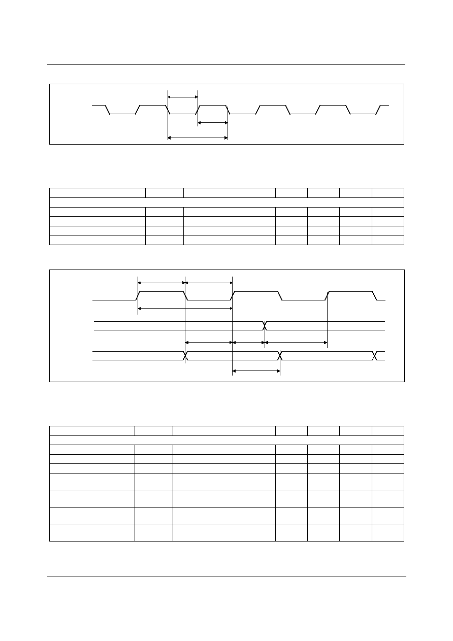
MASTER CLOCK TIMING
MCLK
t
MCLKL
t
MCLKH
t
MCLKY
Figure 1 Master Clock Timing Requirements
Test Conditions
AVDD, DVDD = 5V, AGND = 0V, DGND = 0V, T
A
= +25
o
C, fs = 48kHz, MCLK = 256fs unless otherwise stated.
PARAMETER
SYMBOL
TEST CONDITIONS
MIN
TYP
MAX
UNIT
System Clock Timing Information
MCLK Master clock pulse width high
t
MCLKH
13
ns
MCLK Master clock pulse width low
t
MCLKL
13
ns
MCLK Master clock cycle time
t
MCLKY
26
ns
MCLK Duty cycle
40:60
60:40
DIGITAL AUDIO INTERFACE
BCKIN
LRCIN
t
BCH
t
BCL
t
BCY
DIN
t
LRSU
t
DS
t
LRH
t
DH
Figure 2 Digital Audio Data Timing
Test Conditions
AVDD, DVDD = 5V, AGND = 0V, AGND, DGND = 0V, T
A
= +25
o
C, fs = 48kHz, MCLK = 256fs unless otherwise stated.
PARAMETER
SYMBOL
TEST CONDITIONS
MIN
TYP
MAX
UNIT
Audio Data Input Timing Information
BCKIN cycle time
t
BCY
40
ns
BCKIN pulse width high
t
BCH
16
ns
BCKIN pulse width low
t
BCL
16
ns
LRCIN set-up time to
BCKIN rising edge
t
LRSU
8
ns
LRCIN hold time from
BCKIN rising edge
t
LRH
8
ns
DIN set-up time to BCKIN
rising edge
t
DS
8
ns
DIN hold time from BCKIN
rising edge
t
DH
8
ns

WM8729
Product Preview
WOLFSON MICROELECTRONICS LTD
PP Rev 1.2 April 2001
7
DEVICE DESCRIPTION
INTRODUCTION
The WM8729 is a high performance DAC designed for digital consumer audio applications. Its
range of features make it ideally suited for use in DVD players, AV receivers and other high end
consumer audio equipment.
The WM8729 is a complete 2-channel stereo audio digital-to-analogue converter, including digital
interpolation filter, multi-bit sigma delta with dither, and switched capacitor multi-bit stereo DAC
and output smoothing filters. It is fully compatible and an ideal partner for a range of industry
standard microprocessors, controllers and DSPs.
Control of internal functionality of the device is provided by hardware control (pin programmed).
Operation using master clocks of 256fs, 384fs, 512fs or 768fs is provided, selection between
clock rates being automatically controlled. Sample rates (fs) from less than 8ks/s to 96ks/s are
allowed, provided the appropriate system clock is input. Support is also provided for up to 192ks/s
using a master clock of 128fs or 192fs.
The audio data interface supports right justified or I
2
S (Philips left justified, one bit delayed)
interface formats.
The device is packaged in a small 16-pin SOIC.
CLOCKING SCHEMES
In a typical digital audio system there is only one central clock source producing a reference clock
to which all audio data processing is synchronised. This clock is often referred to as the audio
system's Master Clock. The external master clock can be applied directly through the MCLK input
pin with no configuration necessary for sample rate selection.
Note that on the WM8729, MCLK is used to derive clocks for the DAC path. The DAC path
consists of DAC sampling clock, DAC digital filter clock and DAC digital audio interface timing. In
a system where there are a number of possible sources for the reference clock it is recommended
that the clock source with the lowest jitter be used to optimise the performance of the DAC.
DIGITAL AUDIO INTERFACE
Audio data is applied to the internal DAC filters via the Digital Audio Interface. Two popular
interface formats are supported:
Right Justified mode
I
2
S mode
Both formats send the MSB first. The WM8729 supports word lengths of 16 or 24 bits in I
2
S
mode and 16 or 20 bits in right justified mode. In right justified and I
2
S modes, the digital audio
interface receives data on the DIN input. Audio Data is time multiplexed with LRCIN indicating
whether the left or right channel is present. LRCIN is also used as a timing reference to indicate
the beginning or end of the data words.
In right justified and I
2
S modes, the minimum number of BCKINs per LRCIN period is 2 times the
selected word length. LRCIN must be high for a minimum of word length BCKINs and low for a
minimum of word length BCKINs. Any mark to space ratio on LRCIN is acceptable provided the
above requirements are met.
WM8729
Product Preview
WOLFSON MICROELECTRONICS LTD
PP Rev 1.2 April 2001
8
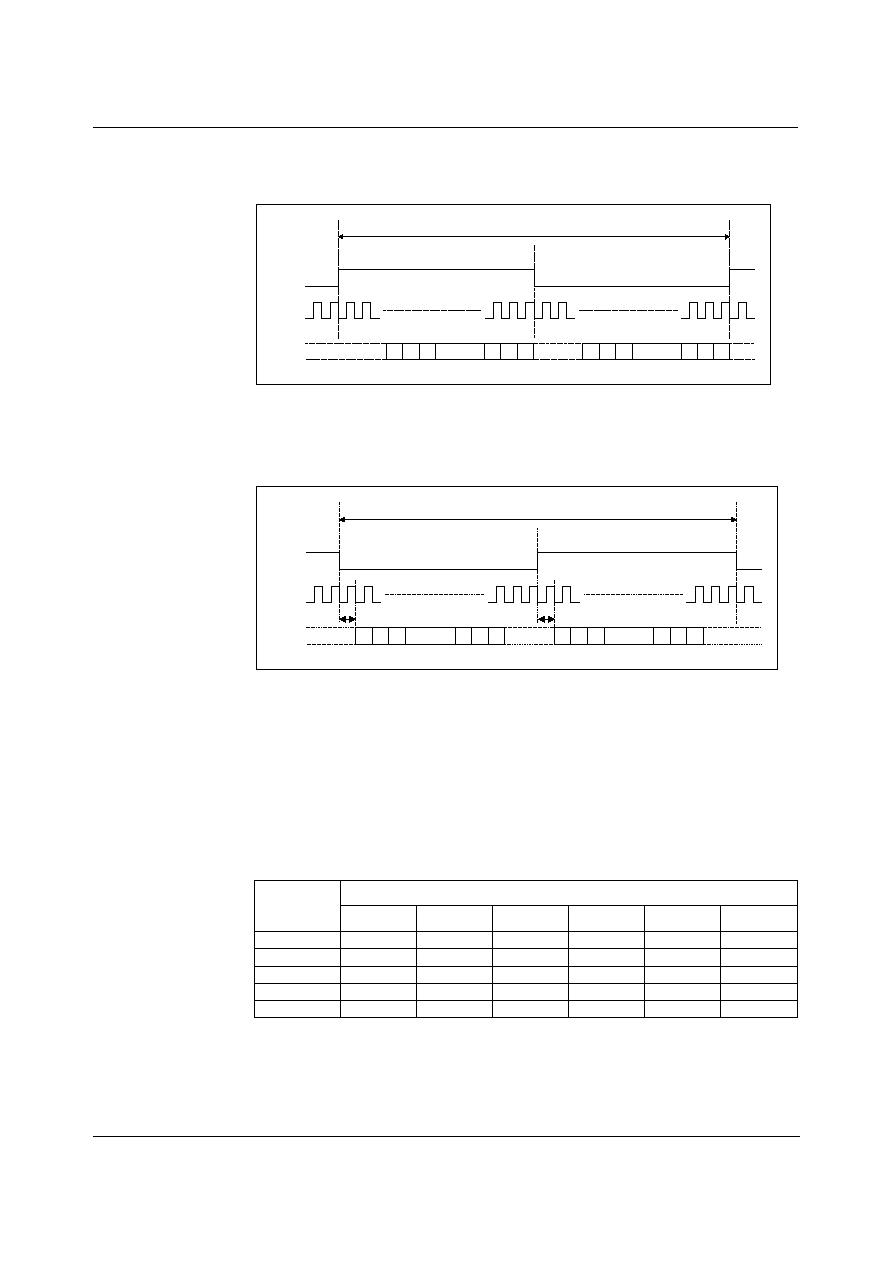
RIGHT JUSTIFIED MODE
In right justified mode, the LSB is sampled on the rising edge of BCKIN preceding a LRCIN
transition. LRCIN is high during the left samples and low during the right samples.
LEFT CHANNEL
RIGHT CHANNEL
LRCIN
BCKIN
DIN
1/fs
n
3
2
1
n-2 n-1
LSB
MSB
n
3
2
1
n-2 n-1
LSB
MSB
Figure 3 Right Justified Mode Timing Diagram
I
2
S MODE
In I
2
S mode, the MSB is sampled on the second rising edge of BCKIN following a LRCIN
transition. LRCIN is low during the left samples and high during the right samples.
LEFT CHANNEL
RIGHT CHANNEL
LRCIN
BCKIN
DIN
1/fs
n
3
2
1
n-2 n-1
LSB
MSB
n
3
2
1
n-2 n-1
LSB
MSB
1 BCKIN
1 BCKIN
Figure 4 I
2
S Mode Timing Diagram
AUDIO DATA SAMPLING RATES
The master clock for WM8729 supports audio sampling rates from 128fs to 768fs, where fs is the
audio sampling frequency (LRCIN) typically 32kHz, 44.1kHz, 48kHz, 96kHz or 192kHz. The
master clock is used to operate the digital filters and the noise shaping circuits.
The WM8729 has a master clock detection circuit that automatically determines the relation
between the master clock frequency and the sampling rate (to within +/- 8 master clocks). If there
is a greater than 8 clocks error, the interface shuts down the DAC and mutes the output. The
master clock should be synchronised with LRCIN, although the WM8729 is tolerant of phase
differences or jitter on this clock.
MASTER CLOCK FREQUENCY (MHZ) (MCLK)
SAMPLING
RATE
(LRCIN)
128fs
192fs
256fs
384fs
512fs
768fs
32kHz
4.096
6.144
8.192
12.288
16.384
24.576
44.1kHz
5.6448
8.467
11.2896
16.9340
22.5792
33.8688
48kHz
6.114
9.216
12.288
18.432
24.576
36.864
96kHz
12.288
18.432
24.576
36.864
Unavailable
Unavailable
192kHz
24.576
36.864
Unavailable
Unavailable
Unavailable
Unavailable
Table 1 Master Clock Frequencies Versus Sampling Rate
WM8729
Product Preview
WOLFSON MICROELECTRONICS LTD
PP Rev 1.2 April 2001
9
HARDWARE CONTROL MODES
The WM8729 is hardware programmable providing the user with options to select input audio data
format, de-emphasis and mute.
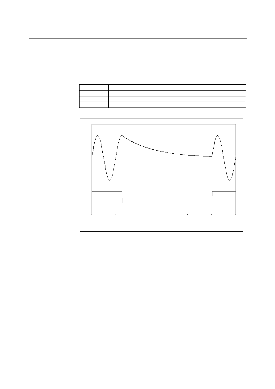
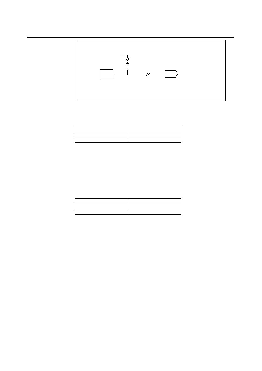
MUTE AND AUTOMUTE OPERATION
Pin 14 (MUTEB) controls selection of MUTE directly, and can be used to enable and disable the
automute function, or as an output of the automuted signal.
MUTEB PIN
DESCRIPTION
0
Mute DAC channels
1
Normal Operation
Floating
Enable IZD, MUTEB becomes an output to indicate when IZD occurs.
Table 2 Mute and Automute Control
-2.5
-2
-1.5
-1
-0.5
0
0.5
1
1.5
0
0.001
0.002
0.003
0.004
0.005
0.006
Time(s)
Figure 5 Application and Release of MUTEB
The MUTEB pin is an input to select mute or not mute. MUTEB is active low; taking the pin low
causes the filters to soft mute, ramping down the audio signal over a few milliseconds. Taking
MUTEB high again allows data into the filter. Refer to Figure 5.
The Infinite Zero Detect (IZD) function detects a series of zero value audio samples of 1024
samples long being applied to both channels. After such an event, a latch is set whose output
(AUTOMUTED) is connected through a 10kohm resistor to the MUTEB pin. Thus if the MUTEB
pin is not being driven, the automute function will assert mute.
If MUTEB is tied high, AUTOMUTED is overridden and will not mute. If MUTEB is driven from a
bi-directional source, then both MUTE and automute functions are available. If MUTEB is not
driven, AUTOMUTED appears as a weak output (10k source impedance) so can be used to drive
external mute circuits. AUTOMUTED will be removed as soon as any channel receives a non-zero
input.
A diagram showing how the various Mute modes interact is shown below in Figure 6.
WM8729
Product Preview
WOLFSON MICROELECTRONICS LTD
PP Rev 1.2 April 2001
10
AUTOMUTED
(Internal Signal)
10k
SOFTMUTE
(Internal Signal)
MUTEB
PIN
Figure 6 Selection Logic for MUTE Modes
INPUT FORMAT SELECTION
FORMAT (pin 16) controls the data input format.
FORMAT
INPUT DATA MODE
0
20-bit right justified (note 2)
1
24-bit I
2
S (note 2)
Table 3 Input Format Selection
Notes:
1.
In 24 bit I
2
S mode, any width of 24 bits or more is supported provided that LRCIN is high for
a minimum of 24 BCKINs and low for a minimum of 24 BCKINs, unless Note 2.
2.
If exactly 16 BCKIN cycles occur in both the low and high period of LRCIN the WM8729 will
assume the data is 16 bit and accept the data accordingly.
DE-EMPHASIS CONTROL
DEM (pin 15) is an input control for selection of de-emphasis filtering to be applied.
DEM
DE-EMPHASIS
0
Off
1
On
Table 4 De-emphasis Control

WM8729
Product Preview
WOLFSON MICROELECTRONICS LTD
PP Rev 1.2 April 2001
11
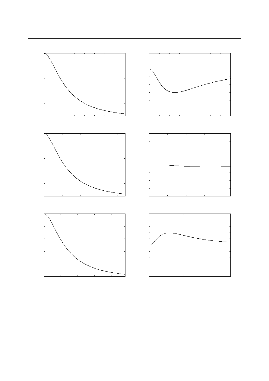
DIGITAL FILTER CHARACTERISTICS
PARAMETER
SYMBOL
TEST CONDITIONS
MIN
TYP
MAX
UNIT
Passband Edge
-3dB
0.487fs
Passband Ripple
f < 0.444fs
�
0.05
dB
Stopband Attenuation
f > 0.555fs
-60
dB
Table 5 Digital Filter Characteristics
DAC FILTER RESPONSES
-120
-100
-80
-60
-40
-20
0
0
0.5
1
1.5
2
2.5
3
Response (dB)
Frequency (Fs)
Figure 7 DAC Digital Filter Frequency Response
-44.1, 48 and 96kHz
-0.2
-0.15
-0.1
-0.05
0
0.05
0.1
0.15
0.2
0
0.05
0.1
0.15
0.2
0.25
0.3
0.35
0.4
0.45
0.5
Response (dB)
Frequency (Fs)
Figure 8 DAC Digital Filter Ripple -44.1, 48 and 96kHz
-80
-60
-40
-20
0
0
0.2
0.4
0.6
0.8
1
Response (dB)
Frequency (Fs)
Figure 9 DAC Digital Filter Frequency Response -192kHz
-1
-0.8
-0.6
-0.4
-0.2
0
0.2
0
0.05
0.1
0.15
0.2
0.25
0.3
0.35
0.4
0.45
0.5
Response (dB)
Frequency (Fs)
Figure 10 DAC Digital Filter Ripple -192kHz
WM8729
Product Preview
WOLFSON MICROELECTRONICS LTD
PP Rev 1.2 April 2001
12
DIGITAL DE-EMPHASIS CHARACTERISTICS
-10
-8
-6
-4
-2
0
0
2
4
6
8
10
12
14
16
Response (dB)
Frequency (kHz)
Figure 11 De-Emphasis Frequency Response (32kHz)
-3
-2.5
-2
-1.5
-1
-0.5
0
0.5
1
0
2
4
6
8
10
12
14
16
Response (dB)
Frequency (kHz)
Figure 12 De-Emphasis Error (32kHz)
-10
-8
-6
-4
-2
0
0
5
10
15
20
Response (dB)
Frequency (kHz)
Figure 13 De-Emphasis Frequency Response (44.1kHz)
-0.4
-0.3
-0.2
-0.1
0
0.1
0.2
0.3
0.4
0
5
10
15
20
Response (dB)
Frequency (kHz)
Figure 14 De-Emphasis Error (44.1kHz)
-10
-8
-6
-4
-2
0
0
5
10
15
20
Response (dB)
Frequency (kHz)
Figure 15 De-Emphasis Frequency Response (48kHz)
-1
-0.8
-0.6
-0.4
-0.2
0
0.2
0.4
0.6
0.8
1
0
5
10
15
20
Response (dB)
Frequency (kHz)
Figure 16 De-Emphasis Error (48kHz)

WM8729
Product Preview
WOLFSON MICROELECTRONICS LTD
PP Rev 1.2 April 2001
13
RECOMMENDED EXTERNAL COMPONENTS
DVDD
DGND
AGND
AVDD
VMID
C
9
C
8
AGND
6
5
Hardware Control
WM8729
Notes:
1. AGND and DGND should be connected as close to the WM8729 as possible.
2. C
2
, C
3
, C
4
and C
8
should be positioned as close to the WM8729 as possible.
3. Capacitor types should be carefully chosen. Capacitors with very low ESR are
recommended for optimum performance.
VREFP
VREFN
C
3
C
4
C
5
C
2
DVDD
C
1
16
FORMAT
15
DEM
VOUTR
10
C
6
VOUTL
C
7
AC-Coupled
VOUTR/L
to External LPF
14
MUTEB
7
AVDD
4
MCLK
3
BCKIN
2
DIN
Audio Serial Data I/F
DGND
AGND
1
LRCIN
9
13
8
12
+
+
+
11
+
+
Figure 17 External Component Diagram
RECOMMENDED EXTERNAL COMPONENTS VALUES
COMPONENT
REFERENCE
SUGGESTED
VALUE
DESCRIPTION
C1 and C5
10
�
F
De-coupling for DVDD and AVDD/VREFP
C2 to C4
0.1
�
F
De-coupling for DVDD and AVDD/VREFP
C6 and C7
10
�
F
Output AC coupling caps to remove midrail DC level from outputs.
C8
0.1
�
F
C9
10
�
F
Reference de-coupling capacitors for VMID pin.
Table 6 External Components Description
WM8729
Product Preview
WOLFSON MICROELECTRONICS LTD
PP Rev 1.2 April 2001
14
RECOMMENDED ANALOGUE LOW PASS FILTER (OPTIONAL)
+
_
+
+VS
-VS
10uF
51
7.5K
680pF
1.8k
47k
4.7k
4.7k
1.0nF
Figure 18 Recommended Low Pass Filter (Optional)

WM8729
Product Preview
WOLFSON MICROELECTRONICS LTD
PP Rev 1.2 April 2001
15
PACKAGE DRAWING
NOTES:
A. ALL LINEAR DIMENSIONS ARE IN MILLIMETERS (INCHES).
B. THIS DRAWING IS SUBJECT TO CHANGE WITHOUT NOTICE.
C. BODY DIMENSIONS DO NOT INCLUDE MOLD FLASH OR PROTRUSION, NOT TO EXCEED 0.25MM (0.010IN).
D. MEETS JEDEC.95 MS-012, VARIATION = AC. REFER TO THIS SPECIFICATION FOR FURTHER DETAILS.
Symbols
Dimensions
(mm)
Dimensions
(Inches)
MIN
MAX
MIN
MAX
A
1.35
1.75
0.0532
0.0688
A1
0.10
0.25
0.0040
0.0098
B
0.33
0.51
0.0130
0.0200
C
0.19
0.25
0.0075
0.0098
D
9.80
10.00
0.3859
0.3937
E
3.80
4.00
0.1497
0.1574
e
1.27 BSC
0.05 BSC
H
5.80
6.20
0.2284
0.2440
h
0.25
0.50
0.0099
0.0196
L
0.40
1.27
0.0160
0.0500
0
o
8
o
0
o
8
o
REF:
JEDEC.95, MS-012
DM012.B
D: 16 PIN SOIC 3.9mm Body
L
C
h x 45
o
0.10 (0.004)
SEATING PLANE
A
A1
-C-
E
H
B
9
16
e
8
1
D