Document Outline
- WM8738
- DESCRIPTION
- FEATURES
- APPLICATIONS
- BLOCK DIAGRAM
- TABLE OF CONTENTS
- PIN CONFIGURATION
- ORDERING INFORMATION
- PIN DESCRIPTION
- ABSOLUTE MAXIMUM RATINGS
- RECOMMENDED OPERATING CONDITIONS
- ELECTRICAL CHARACTERISTICS
- DIGITAL AUDIO INTERFACE TIMING
- DEVICE DESCRIPTION
- INTRODUCTION
- ADC
- ADC DIGITAL FILTER
- AUDIO DATA SAMPLING RATES
- DIGITAL AUDIO INTERFACES
- DIGITAL FILTER CHARACTERISTICS
- ADC FILTER RESPONSES
- ADC HIGH PASS FILTER
- APPLICATIONS INFORMATION
- RECOMMENDED EXTERNAL COMPONENTS
- RECOMMENDED EXTERNAL COMPONENTS VALUES
- PACKAGE DIMENSIONS
- IMPORTANT NOTICE
- ADDRESS:
w
WM8738
24 Bit Stereo ADC
WOLFSON MICROELECTRONICS plc
www.wolfsonmicro.com
Production Data, November 2004, Rev 4.3
Copyright
2004 Wolfson Microelectronics plc
DESCRIPTION
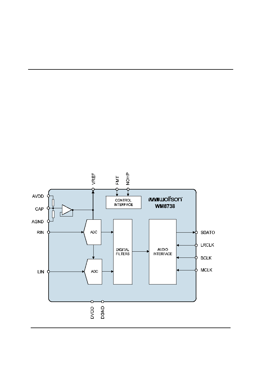
The WM8738 is a high performance stereo audio ADC
designed for consumer applications.
Stereo line-level audio inputs are provided, along with a
control input pin to allow operation of the audio interface in
either one of two industry standard modes. The device also
has a selectable digital high pass filter to remove residual
DC offsets.
Stereo 24-bit multi-bit sigma delta ADCs are provided, along
with oversampling digital interpolation filters. 24-bit digital
audio output word lengths and sampling rates from 32kHz
to 96kHz are supported.
The device is available in a small 14-pin SOIC package.
FEATURES
∑
Audio
Performance
-
90 dB SNR (`A' weighted @ 48kHz)
∑
3.0 ≠ 5.5V Analogue Supply Operation
∑
3.0 ≠ 3.6V Digital Supply Operation
∑
ADC Sampling Frequency: 32kHz ≠ 96kHz
∑
Selectable ADC High Pass Filter
∑
Selectable Audio Data Interface Modes
-
I
2
S or Left Justified
∑
14-pin SOIC Package
APPLICATIONS
∑
CD and Minidisc Recorders
∑
DVD
Players
∑
General Purpose Audio Conversion
BLOCK DIAGRAM

WM8738
Production Data
w
PD Rev 4.3 November 2004
2
TABLE OF CONTENTS
DESCRIPTION .......................................................................................................1
FEATURES.............................................................................................................1
APPLICATIONS .....................................................................................................1
BLOCK DIAGRAM .................................................................................................1
TABLE OF CONTENTS .........................................................................................2
PIN CONFIGURATION...........................................................................................3
ORDERING INFORMATION ..................................................................................3
PIN DESCRIPTION ................................................................................................4
ABSOLUTE MAXIMUM RATINGS .........................................................................5
RECOMMENDED OPERATING CONDITIONS .....................................................5
ELECTRICAL CHARACTERISTICS ......................................................................6
TERMINOLOGY .....................................................................................................7
DIGITAL AUDIO INTERFACE TIMING ..................................................................8
DEVICE DESCRIPTION .........................................................................................9
INTRODUCTION ........................................................................................................... 9
ADC............................................................................................................................... 9
ADC DIGITAL FILTER................................................................................................... 9
AUDIO DATA SAMPLING RATES............................................................................... 10
DIGITAL AUDIO INTERFACES................................................................................... 11
DIGITAL FILTER CHARACTERISTICS ...............................................................12
ADC FILTER RESPONSES .................................................................................12
ADC HIGH PASS FILTER ........................................................................................... 12
APPLICATIONS INFORMATION .........................................................................13
RECOMMENDED EXTERNAL COMPONENTS .......................................................... 13
RECOMMENDED EXTERNAL COMPONENTS VALUES ........................................... 13
PACKAGE DIMENSIONS ....................................................................................14
IMPORTANT NOTICE ..........................................................................................15
ADDRESS: .................................................................................................................. 15
WM8738
Production Data
w
PD Rev 4.3 November 2004
3
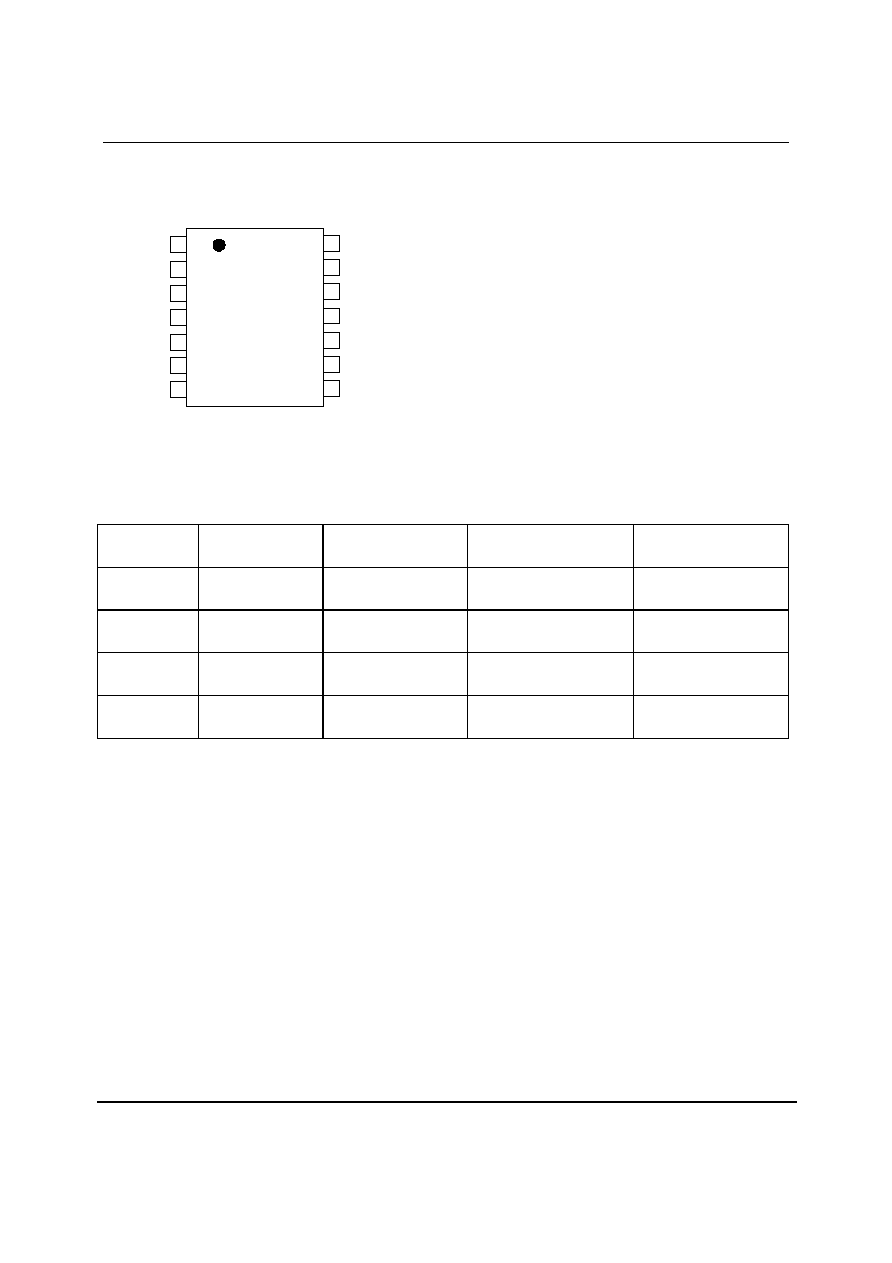
PIN CONFIGURATION
WM8738
1
2
3
4
5
6
7
MCLK
LIN
AVDD
AGND
LRCLK
NOHP
SDATO
DGND
CAP
FMT
BCLK
DVDD
8
9
10
11
14
13
12
RIN
VREF
ORDERING INFORMATION
DEVICE
TEMPERATURE
RANGE
PACKAGE
MOISTURE SENSITIVITY
LEVEL
PEAK SOLDERING
TEMPERATURE
WM8738ED
-25 to +85
o
C
14-pin SOIC
MSL 1
240∞C
WM8738ED/R
-25 to +85
o
C
14-pin SOIC
(tape and reel)
MSL 1
240∞C
WM8738GED/V
-25 to +85
o
C
14-pin SOIC
(lead free)
MSL 2
260∞C
WM8738GED/RV
-25 to +85
o
C
14-pin SOIC
(lead free, tape and reel)
MSL 2
260∞C
Note:
Reel quantity = 3,000
WM8738
Production Data
w
PD Rev 4.3 November 2004
4
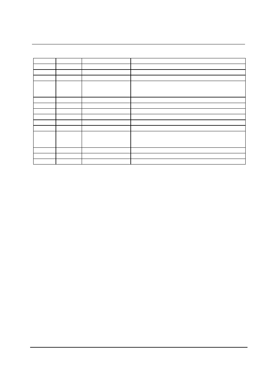
PIN DESCRIPTION
PIN NAME
TYPE
DESCRIPTION
1 DVDD
Supply
Digital positive supply
2 SDATO Digital
Output ADC digital data output
3 BCLK
Digital
Input ADC audio interface data clock (5V tolerant)
4
FMT
Digital input (with pull down)
Audio interface format selection (5V tolerant)
`0' = I
2
S
`1' = Left Justified
5 CAP
Analog
Reference de-coupling pin
6 VREF Analogue
output
Buffered reference decoupling pin
7 RIN Analogue
Input
Right channel ADC input
8 LIN Analogue
Input
Left channel ADC input
9 AVDD
Supply
Analogue positive supply
10 AGND
Supply
Analogue ground supply and chip substrate
11
NOHP
Digital input (with pull down)
Digital highpass filter bypass; (5V tolerant)
`0' = Enabled
`1' = Bypassed
12 LRCLK
Digital
Input
Data left/right word clock (5V tolerant)
13 MCLK
Digital
Input Master clock input (5V tolerant)
14 DGND
Supply
Digital supply ground
Notes
1. Digital input pins have Schmitt trigger input buffers and are 5V tolerant.
WM8738
Production Data
w
PD Rev 4.3 November 2004
5
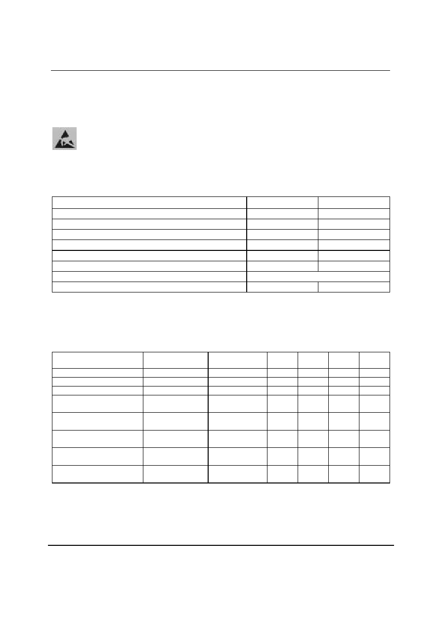
ABSOLUTE MAXIMUM RATINGS
Absolute Maximum Ratings are stress ratings only. Permanent damage to the device may be caused by continuously operating at
or beyond these limits. Device functional operating limits and guaranteed performance specifications are given under Electrical
Characteristics at the test conditions specified.
ESD Sensitive Device. This device is manufactured on a CMOS process. It is therefore generically susceptible
to damage from excessive static voltages. Proper ESD precautions must be taken during handling and storage
of this device.
Wolfson tests its package types according to IPC/JEDEC J-STD-020B for Moisture Sensitivity to determine acceptable storage
conditions prior to surface mount assembly. These levels are:
MSL1 = unlimited floor life at <30
∞
C / 85% Relative Humidity. Not normally stored in moisture barrier bag.
MSL2 = out of bag storage for 1 year at <30
∞
C / 60% Relative Humidity. Supplied in moisture barrier bag.
MSL3 = out of bag storage for 168 hours at <30
∞
C / 60% Relative Humidity. Supplied in moisture barrier bag.
CONDITION
MIN MAX
Digital supply voltage
-0.3V +4.2V
Analogue supply voltage
-0.3V +7.0V
Voltage range digital inputs
DGND -0.3V
+7.0V
Voltage range analogue inputs
AGND -0.3V
AVDD +0.3V
Master Clock Frequency
37MHz
Operating temperature range, T
A
-25
∞
C +85
∞
C
Storage temperature prior to soldering
30
∞
C max / 85% RH max
Storage temperature after soldering
-65
∞
C +150
∞
C
Notes
1.
Analogue and digital grounds must always be within 0.3V of each other.
2.
The digital supply voltage must always be less than or equal to the analogue supply voltage.
RECOMMENDED OPERATING CONDITIONS
PARAMETER SYMBOL
TEST
CONDITIONS
MIN TYP MAX UNIT
Digital supply range
DVDD
3.0
3.6 V
Analogue supply range
AVDD
3.0
5.5 V
Ground
DGND,AGND
0
V
Analogue supply current
AVDD = 5.0V,
(DVDD at 3.3V)
30
mA
Analogue supply current
AVDD = 3.3V,
(DVDD at 3.3V)
19
mA
Supply Current Low Power
Mode
AVDD
=
5.0V
(DVDD at 3.3V)
180
µ
A
Supply Current Low Power
Mode
AVDD
=
3.3V
(DVDD at 3.3V)
110
µ
A
Digital supply current
DVDD
=
3.3V
AVDD = 5.0V or 3.3V
4
mA