
WM8750L
Stereo CODEC for Portable Audio Applications
WOLFSON MICROELECTRONICS plc
www.wolfsonmicro.com
Product Preview, May 2003, Rev 1.77
Copyright
2003 Wolfson Microelectronics plc
DESCRIPTION
The WM8750L is a low power, high quality stereo codec
designed for portable digital audio applications.
The device integrates complete interfaces to stereo or mono
microphones and a stereo headphone. External component
requirements are drastically reduced as no separate
microphone or headphone amplifiers are required.
Advanced on-chip digital signal processing performs
graphic equaliser, 3-D sound enhancement and automatic
level control for the microphone or line input.
The WM8750L can operate as a master or a slave, with
various master clock frequencies including 12 or 24MHz for
USB devices, or standard 256f
s
rates like 12.288MHz and
24.576MHz. Different audio sample rates such as 96kHz,
48kHz, 44.1kHz are generated directly from the master
clock without the need for an external PLL.
The WM8750L operates at supply voltages down to 1.8V,
although the digital core can operate at voltages down to
1.42V to save power, and the maximum for all supplies is
3.6 Volts. Different sections of the chip can also be powered
down under software control.
The WM8750L is supplied in a very small and thin 5x5mm
QFN package, ideal for use in hand-held and portable
systems.
FEATURES
∑
DAC SNR 98dB (`A' weighted), THD -95B at 48kHz, 3.3V
∑
ADC SNR 95dB (`A' weighted), THD -90dB at 48kHz, 3.3V
∑
Complete Stereo / Mono Microphone Interface
- Programmable ALC / Noise Gate
∑
On-chip 400mW BTL Speaker Driver (mono)
∑
On-chip Headphone Driver
-
>40mW output power on 16
/ 3.3V
-
THD ≠80dB at 20mW, SNR 90dB with 16
load
-
No DC blocking capacitors required (capless mode)
∑
Separately mixed mono output
∑
Digital Graphic Equaliser
∑
Low Power
-
7mW stereo playback (1.8V / 1.5V supplies)
-
14mW record & playback (1.8V / 1.5V supplies)
∑
Low Supply Voltages
-
Analogue 1.8V to 3.6V
-
Digital core: 1.42V to 3.6V
-
Digital I/O: 1.8V to 3.6V
∑
256fs / 384fs or USB master clock rates: 12MHz, 24MHz
∑
Audio sample rates: 8, 11.025, 16, 22.05, 24, 32, 44.1, 48,
88.2, 96kHz generated internally from master clock
∑
5x5x0.9mm QFN package
APPLICATIONS
∑
MP3 Player / Recorder
∑
AAC/WMA/Multi-Format Player / Recorder
∑
Minidisc Player / Recorder
∑
Portable Digital Music Systems
BLOCK DIAGRAM
LINSEL
ANALOGUE
MONO MIX
CONTROL
INTERFACE
CSB
SDI
N
SC
L
K
MOD
E
MICBIAS
≈
WM8750L
DCVDD
DBVDD
DGND
LMIXSEL
DAC
ROUT1VOL
LOUT1VOL
MONOVOL
LOUT1
ROUT1
MONOOUT
(phone TX)
LOUT2
ROUT2
VR
EF
AV
DD
AG
ND
VM
ID
50K
50K
HPVDD
HPGND
DAC
AUDIO
INTERFACE
ADC
D
AT
A
D
CL
RC
BC
L
K
MC
L
K
DAC
D
AT
DA
CL
RC
DIGITAL
FILTERS
VOLUME
DIGITAL
MONO MIX
3D
ENHANCE
ADC
ADC
DIGITAL
FILTERS
GRAPHIC
EQUALISER
BASS
BOOST
CLOCK
CIRCUITRY
LINPUT3
LINPUT2
LINPUT1
LI2LO
RI2LO
LI2RO
RI2RO
LI2MO
RI2MO
LD2LO
RD2LO
LD2MO
RD2MO
LD2RO
RD2RO
LEFT
MIXER
RIGHT
MIXER
MONO
MIXER
ROUT2VOL
LOUT2VOL
-1
ROUT2
INV
OUT3
VREF
ROUT1
MONOOUT
-1
L - (-R)
= L+R
PGA
+ MIC
BOOST
M
U
X
M
U
X
DIFF.
INPUT
L1-R1 OR
L2-R2
DC MEASUREMENT
RINSEL
RMIXSEL
RINPUT3/
HPDETECT
RINPUT2
RINPUT1
PGA
+ MIC
BOOST
M
U
X
M
U
X
DC MEASUREMENT
M
U
X
OUT3SW

WM8750L
Product Preview
PP Rev 1.77 May 2003
2
TABLE OF CONTENTS
DESCRIPTION ......................................................................................................1
FEATURES ...........................................................................................................1
APPLICATIONS ....................................................................................................1
BLOCK DIAGRAM................................................................................................1
PIN CONFIGURATION .........................................................................................4
ORDERING INFORMATION .................................................................................4
PIN DESCRIPTION ...............................................................................................4
ABSOLUTE MAXIMUM RATINGS........................................................................5
RECOMMENDED OPERATION CONDITIONS ....................................................5
ELECTRICAL CHARACTERISTICS .....................................................................6
HEADPHONE / SPEAKER OUTPUT THD VERSUS POWER......................................8
POWER CONSUMPTION ...................................................................................11
SIGNAL TIMING REQUIREMENTS....................................................................12
SYSTEM CLOCK TIMING ..........................................................................................12
AUDIO INTERFACE TIMING ≠ MASTER MODE........................................................12
AUDIO INTERFACE TIMING ≠ SLAVE MODE ...........................................................13
DEVICE DESCRIPTION......................................................................................16
INTRODUCTION ........................................................................................................16
INPUT SIGNAL PATH ................................................................................................16
AUTOMATIC LEVEL CONTROL (ALC) ......................................................................22
3D STEREO ENHANCEMENT ...................................................................................25
OUTPUT SIGNAL PATH.............................................................................................26
ANALOGUE OUTPUTS ..............................................................................................31
ENABLING THE OUTPUTS........................................................................................33
HEADPHONE SWITCH ..............................................................................................33
THERMAL SHUTDOWN.............................................................................................35
HEADPHONE OUTPUT..............................................................................................35
DIGITAL AUDIO INTERFACE ....................................................................................36

Product Preview
WM8750L
PP Rev 1.77 May 2003
3
AUDIO INTERFACE CONTROL .................................................................................39
MASTER CLOCK AND AUDIO SAMPLE RATES .......................................................40
CONTROL INTERFACE .............................................................................................42
POWER SUPPLIES....................................................................................................43
POWER MANAGEMENT ............................................................................................44
REGISTER MAP .................................................................................................46
DIGITAL FILTER CHARACTERISTICS..............................................................47
TERMINOLOGY .........................................................................................................47
DAC FILTER RESPONSES ................................................................................48
ADC FILTER RESPONSES ................................................................................49
DE-EMPHASIS FILTER RESPONSES ...............................................................50
HIGHPASS FILTER ............................................................................................51
APPLICATIONS INFORMATION ........................................................................52
RECOMMENDED EXTERNAL COMPONENTS .........................................................52
LINE INPUT CONFIGURATION .................................................................................53
MICROPHONE INPUT CONFIGURATION .................................................................53
MINIMISING POP NOISE AT THE ANALOGUE OUTPUTS .......................................54
POWER MANAGEMENT EXAMPLES........................................................................54
PACKAGE DIMENSIONS ...................................................................................55
IMPORTANT NOTICE........................................................................................ 54
ADDRESS: .................................................................................................................56
WM8750L
Product Preview
PP Rev 1.77 May 2003
4
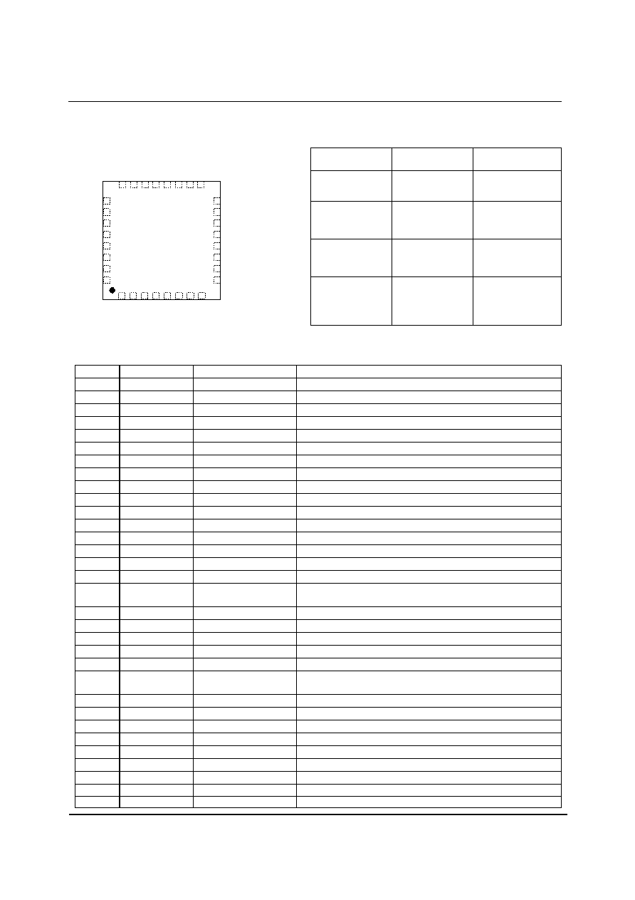
PIN CONFIGURATION
ORDERING INFORMATION
ORDER CODE
TEMPERATURE
RANGE
PACKAGE
WM8750LEFL -25
∞
C to +85
∞
C 32-pin
QFN
(5x5x0.9mm)
WM8750LSEFL -25
∞
C to +85
∞
C 32-pin
QFN
(5x5x0.9mm)
(lead free)
WM8750LEFL/R -25
∞
C to +85
∞
C 32-pin
QFN
(5x5x0.9mm)
(tape and reel)
WM8750LSEFL/R -25
∞
C to +85
∞
C 32-pin
QFN
(5x5x0.9mm)
(lead free, tape and
reel)
1
2
3
4
5
6
7
8
24
23
22
21
20
19
18
17
16
15
14
13
12
11
10
9
25
26
27
28
29
30
31
32
DA
CDA
T
BC
L
K
DCV
DD
DG
N
D
D
BVD
D
MC
L
K
DA
CLRC
OUT3
AVD
D
VMID
AGN
D
VR
EF
MICBI
A
S
RINPUT3 /
HPDETECT
HPGND
ADCLRC
MONOOUT
H
PVD
D
ROUT1
LOUT1
ROUT2
LOUT2
A
DCDA
T
CSB
MODE
LINPUT2
LINPUT1
RINPUT1
RINPUT2
LIN
P
UT
3
SDIN
SCLK
Note:
Reel quantity = 3500
PIN DESCRIPTION
PIN #
NAME
TYPE
DESCRIPTION
1 MCLK
Digital Input
Master Clock
2 DCVDD
Supply Digital
Core
Supply
3 DBVDD
Supply
Digital Buffer (I/O) Supply
4 DGND
Supply
Digital Ground (return path for both DCVDD and DBVDD)
5 BCLK
Digital Input / Output
Audio Interface Bit Clock
6 DACDAT
Digital Input
DAC Digital Audio Data
7 DACLRC
Digital Input / Output
Audio Interface Left / Right Clock/Clock Out
8 ADCDAT
Digital Output
ADC Digital Audio Data
9 ADCLRC
Digital Input / Output
Audio Interface Left / Right Clock
10 MONOOUT
Analogue Output
Mono Output
11 OUT3
Analogue Output
Analogue Output 3 (can be used as Headphone Pseudo Ground)
12 ROUT1
Analogue Output
Right Output 1 (Line or Headphone)
13 LOUT1
Analogue Output
Left Output 1 (Line or Headphone)
14 HPGND
Supply
Supply for Analogue Output Drivers (LOUT1/2, ROUT1/2)
15 ROUT2
Analogue Output
Right Output 1 (Line or Headphone or Speaker)
16 LOUT2
Analogue Output
Left Output 1 (Line or Headphone or Speaker)
17 HPVDD
Supply
Supply for Analogue Output Drivers (LOUT1/2, ROUT1/2,
MONOUT)
18 AVDD
Supply Analogue
Supply
19 AGND
Supply
Analogue Ground (return path for both AVDD and MVDD)
20 VREF
Analogue Output
Reference Voltage Decoupling Capacitor
21 VMID
Analogue Output
Midrail Voltage Decoupling Capacitor
22 MICBIAS
Analogue Output
Microphone Bias
23 RINPUT3
/
HPDETECT
Analogue Input
Right Channel Input 3 or Headphone Plug-in Detection
24 LINPUT3
Analogue Input
Left Channel Input 3
25 RINPUT2
Analogue Input
Right Channel Input 2
26 LINPUT2
Analogue Input
Left Channel Input 2
27 RINPUT1
Analogue Input
Right Channel Input 1
28 LINPUT1
Analogue Input
Left Channel Input 1
29
MODE
Digital Input
Control Interface Selection
30 CSB
Digital Input
Chip Select / Device Address Selection
31 SDIN
Digital Input/Output
Control Interface Data Input / 2-wire Acknowledge output
32
SCLK
Digital Input
Control Interface Clock Input
Product Preview
WM8750L
PP Rev 1.77 May 2003
5
ABSOLUTE MAXIMUM RATINGS
Absolute Maximum Ratings are stress ratings only. Permanent damage to the device may be caused by continuously
operating at or beyond these limits. Device functional operating limits and guaranteed performance specifications are given
under Electrical Characteristics at the test conditions specified.
ESD Sensitive Device. This device is manufactured on a CMOS process. It is therefore generically susceptible
to damage from excessive static voltages. Proper ESD precautions must be taken during handling and storage
of this device.
The WM8750L has been classified as MSL1, which has an unlimited floor life at <30
o
C / 85% Relative Humidity and therefore will
not be supplied in moisture barrier bags.
CONDITION MIN
MAX
Supply voltages
-0.3V +3.63V
Voltage range digital inputs
DGND -0.3V
DBVDD +0.3V
Voltage range analogue inputs
AGND -0.3V
AVDD +0.3V
Operating temperature range, T
A
-25
∞
C +85
∞
C
Storage temperature prior to soldering
30
∞
C max / 85% RH max
Storage temperature after soldering
-65
∞
C +150
∞
C
Package body temperature (soldering 10 seconds)
+260
∞
C
Package body temperature (soldering 2 minutes)
+183
∞
C
Notes
1.
Analogue and digital grounds must always be within 0.3V of each other.
2.
All digital and analogue supplies are completely independent from each other.
3.
DCVDD must be less than or equal to AVDD & DBVDD.
RECOMMENDED OPERATION CONDITIONS
PARAMETER SYMBOL
MIN
TYP
MAX
UNIT
Digital supply range (Core)
DCVDD 1.42
2.0
3.6
V
Digital supply range (Buffer)
DBVDD 1.8
2.0
3.6
V
Analogue supplies range
AVDD, HPVDD
1.8
2.0
3.6
V
Ground
DGND,AGND, HPGND
0
V