 | –≠–ª–µ–∫—Ç—Ä–æ–Ω–Ω—ã–π –∫–æ–º–ø–æ–Ω–µ–Ω—Ç: WM8772 | –°–∫–∞—á–∞—Ç—å:  PDF PDF  ZIP ZIP |
Document Outline
- WM8772
- 24-bit, 192kHz 6-Channel Codec with Volume Control
- DESCRIPTION
- FEATURES
- APPLICATIONS
- BLOCK DIAGRAM - 28 PIN SSOP
- BLOCK DIAGRAM Ö 32 PIN TQFP
- TABLE OF CONTENTS
- PIN CONFIGURATION - 28 LEAD SSOP
- ORDERING INFORMATION
- PIN CONFIGURATION
- ORDERING INFORMATION
- PIN DESCRIPTION Ö 28 LEAD SSOP
- PIN DESCRIPTION Ö 32 LEAD TQFP
- ABSOLUTE MAXIMUM RATINGS
- RECOMMENDED OPERATING CONDITIONS
- ELECTRICAL CHARACTERISTICS
- TERMINOLOGY
- DIGITAL FILTER CHARACTERISTICS
- DAC FILTER RESPONSES
- ADC FILTER RESPONSES
- DIGITAL DE-EMPHASIS CHARACTERISTICS
- ADC HIGH PASS FILTER
- PAGES 12 TO 36 DESCRIBE THE OPERATION OF THE WM8772EDS 28 PIN
- PAGES 37 TO 66 DESCRIBE THE OPERATION OF THE WM8772EFT 32 PIN
- WM8772EDS Ö 28 PIN SSOP
- MPU INTERFACE TIMING
- DIGITAL AUDIO INTERFACE Ö SLAVE MODE
- DIGITAL AUDIO INTERFACE Ö MASTER MODE
- MASTER CLOCK TIMING
- DEVICE DESCRIPTION
- INTRODUCTION
- AUDIO DATA SAMPLING RATES
- HARDWARE CONTROL MODES
- DIGITAL AUDIO INTERFACE
- POWERDOWN MODES
- ZERO DETECT
- SOFTWARE CONTROL INTERFACE OPERATION
- REGISTER MAP - 28 PIN SSOP
- CONTROL INTERFACE REGISTERS
- APPLICATIONS INFORMATION
- RECOMMENDED EXTERNAL COMPONENTS
- RECOMMENDED EXTERNAL COMPONENTS VALUES
- SUGGESTED ANALOGUE LOW PASS POST DAC FILTERS
- PACKAGE DIMENSIONS
- WM8722EFT - 32 PIN TQFP
- MASTER CLOCK TIMING
- DIGITAL AUDIO INTERFACE Ö MASTER MODE
- DIGITAL AUDIO INTERFACE Ö SLAVE MODE
- MPU INTERFACE TIMING
- DEVICE DESCRIPTION
- INTRODUCTION
- AUDIO DATA SAMPLING RATES
- HARDWARE CONTROL MODES
- DIGITAL AUDIO INTERFACE
- POWERDOWN MODES
- ZERO DETECT
- SOFTWARE CONTROL INTERFACE OPERATION
- REGISTER MAP Ö 32 PIN TQFP
- CONTROL INTERFACE REGISTERS
- APPLICATIONS INFORMATION
- RECOMMENDED EXTERNAL COMPONENTS
- RECOMMENDED EXTERNAL COMPONENTS VALUES
- SUGGESTED ANALOGUE LOW PASS POST DAC FILTERS
- PACKAGE DIMENSIONS
- IMPORTANT NOTICE
w
WM8772
24-bit, 192kHz 6-Channel Codec with Volume Control
WOLFSON MICROELECTRONICS plc
w :: www.wolfsonmicro.com
Production Data, October 2004, Rev 4.1
Copyright
2004 Wolfson Microelectronics plc
DESCRIPTION
The WM8772 is a multi-channel audio codec ideal for DVD
and surround sound processing applications for home hi-fi,
automotive and other audio visual equipment.
A stereo 24-bit multi-bit sigma delta ADC is used. Digital
audio output word lengths from 16-32 bits and sampling
rates from 32kHz to 96kHz are supported. The 32-lead
version allows separate ADC and DAC samples rates.
Three stereo 24-bit multi-bit sigma delta DACs are used
with oversampling digital interpolation filters. Digital audio
input word lengths from 16-32 bits and sampling rates from
8kHz to 192kHz are supported. Each DAC channel has
independent digital volume and mute control.
The audio data interface supports I
2
S, left justified, right
justified and DSP digital audio formats.
The device is controlled via a 3 wire serial interface. The
interface provides access to all features including channel
selection, volume controls, mutes, de-emphasis and power
management facilities. The device is available in a 28-pin
SSOP or 32 pin TQFP.
FEATURES
∑
Audio
Performance
-
103dB SNR (`A' weighted @ 48kHz) DAC
-
100dB SNR (`A' weighted @ 48kHz) ADC (TQFP)
∑
DAC Sampling Frequency: 8kHz ≠ 192kHz
∑
ADC Sampling Frequency: 32kHz ≠ 96kHz
∑
ADC and DAC can run at different sample rates (32 pin
TQFP version only)
∑
3-Wire SPI Serial or Hardware Control Interface
∑
Programmable Audio Data Interface Modes
-
I
2
S, Left, Right Justified or DSP
-
16/20/24/32 bit Word Lengths
∑
Three Independent stereo DAC outputs with independent
digital volume controls
∑
Master or Slave Audio Data Interface
∑
2.7V to 5.5V Analogue, 2.7V to 3.6V Digital supply
Operation
∑
28 pin SSOP or 32 pin TQFP Package
APPLICATIONS
∑
DVD
Players
∑
Surround Sound AV Processors and Hi-Fi systems
∑
Automotive
Audio
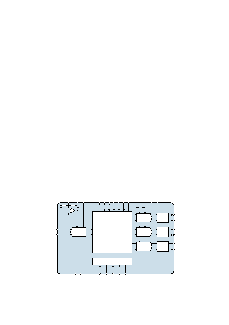
BLOCK DIAGRAM - 28 PIN SSOP
VOUT1L
VOUT1R
VOUT2L
VOUT2R
VOUT3L
VOUT3R
STEREO
ADC
VR
E
F
N
VR
E
F
P
VM
I
D
AUDIO
INTERFACE
&
DIGITAL FILTERS
DO
UT
VREFP
STEREO
DAC
STEREO
DAC
AINL
AINR
RE
FA
DC
AV
D
D
AG
N
D
DV
DD
DG
ND
CONTROL INTERFACE
MD
/D
M
M
C
/IW
L
M
L
/I2
S
WM8772EDS
LOW
PASS
FILTER
LOW
PASS
FILTER
LOW
PASS
FILTER
MO
DE
MU
TE
STEREO
DAC
VREFN
W
VREFN
BC
L
K
LR
C
DI
N1
DI
N2
DI
N3
MC
L
K
WM8772
Production Data
w
PD Rev 4.1 October 2004
2
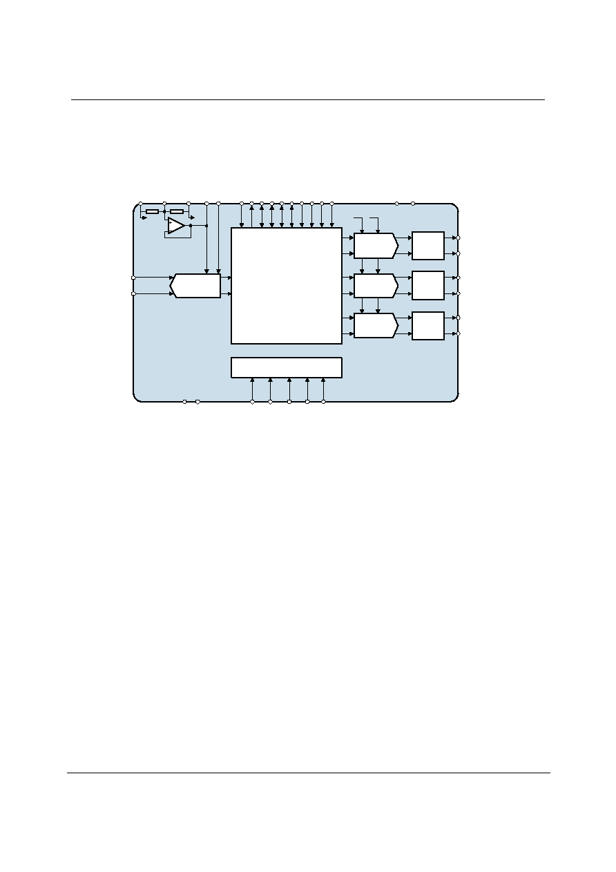
BLOCK DIAGRAM ≠ 32 PIN TQFP
VOUT1L
VOUT1R
VOUT2L
VOUT2R
VOUT3L
VOUT3R
STEREO
ADC
DA
CV
R
E
FN
DA
CV
R
E
FP
VMI
D
AUDIO
INTERFACE
&
DIGITAL FILTERS
A
DCLRC
*
A
DCB
C
L
K
*
DA
CB
C
L
K
*
DA
CLRC
*
DI
N
1
DA
CMCLK
*
DO
UT
VREFP
STEREO
DAC
STEREO
DAC
AINL
AINR
RE
FA
DC
AVD
D
AGN
D
DV
DD
DG
N
D
CONTROL INTERFACE
MD/
D
M
MC
/
I
W
L
ML
/I
2
S
A
DCMCLK
*
WM8772EFT
LOW
PASS
FILTER
LOW
PASS
FILTER
LOW
PASS
FILTER
DI
N
3
DI
N
2
MO
D
E
MUT
E
STEREO
DAC
VREFN
W
A
DCV
R
E
FN
* extra pins on TQFP allow separate
clocking of ADC and DAC

Production Data
WM8772
w
PD Rev 4.1 October 2004
3
TABLE OF CONTENTS
DESCRIPTION .......................................................................................................1
FEATURES.............................................................................................................1
APPLICATIONS .....................................................................................................1
BLOCK DIAGRAM - 28 PIN SSOP ........................................................................1
BLOCK DIAGRAM ≠ 32 PIN TQFP........................................................................2
TABLE OF CONTENTS .........................................................................................3
PIN CONFIGURATION - 28 LEAD SSOP .............................................................5
ORDERING INFORMATION ..................................................................................5
PIN CONFIGURATION 32 LEAD TQFP...............................................................6
ORDERING INFORMATION ..................................................................................6
PIN DESCRIPTION ≠ 28 LEAD SSOP...................................................................7
PIN DESCRIPTION ≠ 32 LEAD TQFP ...................................................................8
ABSOLUTE MAXIMUM RATINGS .........................................................................9
RECOMMENDED OPERATING CONDITIONS ...................................................10
ADC HIGH PASS FILTER ........................................................................................... 14
DIGITAL DE-EMPHASIS CHARACTERISTICS........................................................... 14
WM8772EDS ≠ 28 PIN SSOP ..............................................................................16
MASTER CLOCK TIMING ........................................................................................... 16
DIGITAL AUDIO INTERFACE ≠ MASTER MODE ....................................................... 16
MPU INTERFACE TIMING .......................................................................................... 19
INTRODUCTION ......................................................................................................... 20
AUDIO DATA SAMPLING RATES............................................................................... 20
HARDWARE CONTROL MODES ............................................................................... 21
DIGITAL AUDIO INTERFACE ..................................................................................... 23
POWERDOWN MODES ............................................................................................. 27
ZERO DETECT ........................................................................................................... 27
CONTROL INTERFACE REGISTERS ........................................................................ 29
RECOMMENDED EXTERNAL COMPONENTS .......................................................... 37
SUGGESTED ANALOGUE LOW PASS POST DAC FILTERS ................................... 38
WM8722EFT - 32 PIN TQFP ................................................................................41
MASTER CLOCK TIMING ........................................................................................... 41
DIGITAL AUDIO INTERFACE ≠ MASTER MODE ....................................................... 41
MPU INTERFACE TIMING .......................................................................................... 44
DEVICE DESCRIPTION .......................................................................................46
INTRODUCTION ......................................................................................................... 46
AUDIO DATA SAMPLING RATES............................................................................... 46
HARDWARE CONTROL MODES ............................................................................... 47
DIGITAL AUDIO INTERFACE ..................................................................................... 49
POWERDOWN MODES ............................................................................................. 54
ZERO DETECT ........................................................................................................... 54
SOFTWARE CONTROL INTERFACE OPERATION ...........................................54
REGISTER MAP ≠ 32 PIN TQFP .........................................................................55
CONTROL INTERFACE REGISTERS ........................................................................ 56

WM8772
Production Data
w
PD Rev 4.1 October 2004
4
APPLICATIONS INFORMATION .........................................................................66
RECOMMENDED EXTERNAL COMPONENTS .......................................................... 66
SUGGESTED ANALOGUE LOW PASS POST DAC FILTERS...........................67
PACKAGE DIMENSIONS ....................................................................................69
IMPORTANT NOTICE ..........................................................................................70
ADDRESS: .................................................................................................................. 70
Production Data
WM8772
w
PD Rev 4.1 October 2004
5
PIN CONFIGURATION - 28 LEAD SSOP
1
MODE
2
VMID
3
AINR
4
REFADC
5
AINL
6
VREFP
7
VOUT1L
8
VOUT3R
9
VOUT1R
10
VREFN
VOUT2L
VOUT2R
VOUT3L
AGND
15
DGND
AVDD
DIN2
DIN1
BCLK
LRC
MCLK
DVDD
DOUT
MC/IWL
DIN3
ML/I2S
MD/DM
MUTE
11
12
13
14
16
17
18
19
20
21
22
23
24
25
28
27
26
ORDERING INFORMATION
DEVICE
TEMPERATURE
RANGE
PACKAGE
MOISTURE
SENSITIVITY LEVEL
PEAK SOLDERING
TEMPERATURE
WM8772EDS
-25 to +85
o
C 28-pin
SSOP
MSL1 260
o
C
WM8772EDS/R
-25 to +85
o
C
28-pin SSOP
(tape and reel)
MSL1 260
o
C
WM8772SEDS/V
-25 to +85
o
C
28-pin SSOP
(lead free)
MSL2 260
o
C
WM8772SEDS/RV
-25 to +85
o
C
28-pin SSOP
(lead free, tape
and reel)
MSL2 260
o
C
Note:
Reel quantity = 2,000

WM8772
Production Data
w
PD Rev 4.1 October 2004
6
PIN CONFIGURATION
32 LEAD TQFP
MD/DM
MC/IWL
ML/I2S
DOUT
DIN
3
DIN
2
DIN
1
DVDD
DG
ND
ADCMCLK
DACMLCK
ADCBCLK
DACBCLK
ADCL
RC
VOUT2L
VOUT2R
AGND
VOUT1L
VOUT1R
AVDD
ADCVREFN
VOUT3R
VOUT3L
DACVREFP
AI
NR
AI
NL
REFADC
VM
I
D
23
22
21
20
19
18 17
24
2
3
4
5
6
7
8
1
1
5
1
4
1
3
12
11
10
9
16
MUTE
26
27
28
29
30
31
32
25
DACVREFN
MODE
DACL
RC
ORDERING INFORMATION
DEVICE
TEMPERATURE
RANGE
PACKAGE
MOISTURE SENSITIVITY
LEVEL
PEAK SOLDERING
TEMPERATURE
WM8772EFT
-25 to +85
o
C 32-lead
TQFP
MSL1
240
o
C
WM8772SEFT/V
-25 to +85
o
C 32-lead
TQFP
(lead free)
MSL2 260
o
C
WM8772EFT/R
-25 to +85
o
C 32-lead
TQFP
(tape and reel)
MSL1 240
o
C
WM8772SEFT/RV
-25 to +85
o
C 32-lead
TQFP
(lead free, tape
and reel)
MSL2 260
o
C
Note:
Reel quantity = 2,200

Production Data
WM8772
w
PD Rev 4.1 October 2004
7
PIN DESCRIPTION ≠ 28 LEAD SSOP
PIN NAME TYPE
DESCRIPTION
1 MODE
Digital
input
Control format selection
0 = Software control
1 = Hardware control
2 MCLK
Digital
input
Master clock; 256, 384, 512 or 768fs (fs = word clock frequency)
(combined ADCMCLK and DACMCLK)
3 BCLK
Digital
input/output
Audio interface bit clock (combined ADCBCLK and DACBCLK)
4 LRC
Digital
input/output
Audio left/right word clock (combined ADCLRC and DACLRC)
5 DVDD Supply
Digital positive supply
6 DGND Supply
Digital negative supply
7 DIN1
Digital
input
DAC channel 1 data input
8 DIN2
Digital
input
DAC channel 2 data input
9 DIN3
Digital
input
DAC channel 3 data input
10 DOUT
Digital
output
ADC data output
11 ML/I2S
Digital
input
Software Mode: Serial interface Latch signal
Hardware Mode: Input Audio Data Format
12 MC/IWL
Digital
input
Software Mode: Serial control interface clock
Hardware Mode: Audio data input word length
13 MD/DM
Digital
input
Software Mode: Serial interface data
Hardware Mode: De-emphasis selection
14 MUTE
Digital
input/output
DAC Zero Flag output or DAC mute input
15 REFADC
Analogue
output
ADC reference buffer decoupling pin; 10uF external decoupling
16 VREFN Supply
ADC and DAC negative supply
17 VREFP Supply
DAC positive reference supply
18 VMID
Analogue
output
Midrail divider decoupling pin; 10uF external decoupling
19 AINR
Analogue
input
ADC right input
20 AINL
Analogue
input
ADC left input
21 VOUT1L
Analogue
output
DAC channel 1 left output
22 VOUT1R
Analogue
output
DAC channel 1 right output
23 VOUT2L
Analogue
output
DAC channel 2 left output
24 VOUT2R
Analogue
output
DAC channel 2 right output
25 VOUT3L
Analogue
output
DAC channel 3 left output
26 VOUT3R
Analogue
output
DAC channel 3 right output
27 AGND Supply
Analogue negative supply and substrate connection
28 AVDD Supply
Analogue positive supply
Note: Digital input pins have Schmitt trigger input buffers.

WM8772
Production Data
w
PD Rev 4.1 October 2004
8
PIN DESCRIPTION ≠ 32 LEAD TQFP
PIN NAME
TYPE
DESCRIPTION
1 ADCLRC
Digital
Input/Output
ADC left/right word clock
2 DACLRC
Digital
Input/Output
DAC left/right word clock
3 DVDD Supply
Digital positive supply
4 DGND Supply
Digital negative supply
5 DIN1
Digital
Input
DAC channel 1 data input
6 DIN2
Digital
Input
DAC channel 2 data input
7 DIN3
Digital
Input
DAC channel 3 data input
8 DOUT
Digital
Output
ADC data output
9 ML/I2S
Digital
Input
Software Mode: Serial interface Latch signal
Hardware Mode: Input Audio Data Format
10 MC/IWL Digital
Input
Software Mode: Serial control interface clock
Hardware Mode: Audio data input word length
11 MD/DM Digital
Input
Software Mode: Serial interface data
Hardware Mode: De-emphasis selection
12 MUTE
Digital
Input/Output
DAC Zero Flag output or DAC Mute Input
13
REFADC
Analogue Output
ADC reference buffer decoupling pin; 10uF external decoupling
14 ADCVREFN Supply ADC negative supply
15 DACVREFN Supply DAC negative supply
16 DACVREFP Supply DAC positive reference supply
17
VMID
Analogue Output
Midrail divider decoupling pin; 10uF external decoupling
18 AINR
Analogue
Input
ADC right input
19 AINL
Analogue
Input
ADC left input
20 VOUT1L
Analogue
Output
DAC channel 1 left output
21 VOUT1R
Analogue
Output
DAC channel 1 right output
22 VOUT2L
Analogue
Output
DAC channel 2 left output
23 VOUT2R
Analogue
Output
DAC channel 2 right output
24 VOUT3L
Analogue
Output
DAC channel 3 left output
25 VOUT3R
Analogue
Output
DAC channel 3 right output
26 AGND Supply
Analogue negative supply and substrate connection
27 AVDD Supply
Analogue positive supply
28 MODE Digital
Input
Control format selection
0 = Software control
1 = Hardware control
29 ADCMCLK Digital
Input
Master ADC clock; 256, 384, 512 or 768fs (fs = word clock frequency)
30 DACMCLK Digital
Input
Master DAC clock; 256, 384, 512 or 768fs (fs = word clock frequency)
31 ADCBCLK
Digital
Input/Output
ADC audio interface bit clock
32 DACBCLK
Digital
Input/Output
DAC audio interface bit clock
Note: Digital input pins have Schmitt trigger input buffers.
Production Data
WM8772
w
PD Rev 4.1 October 2004
9
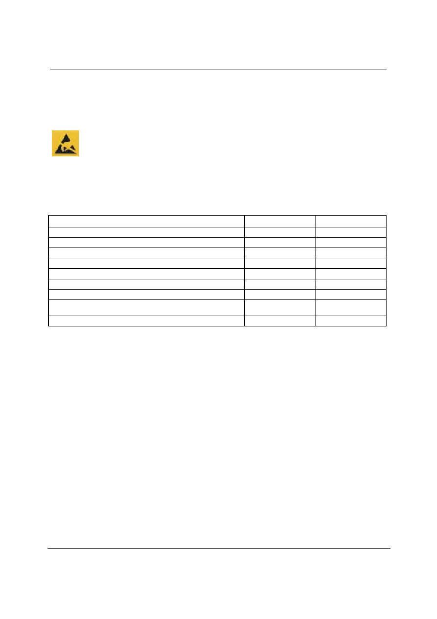
ABSOLUTE MAXIMUM RATINGS
Absolute Maximum Ratings are stress ratings only. Permanent damage to the device may be caused by continuously operating at
or beyond these limits. Device functional operating limits and guaranteed performance specifications are given under Electrical
Characteristics at the test conditions specified.
ESD Sensitive Device. This device is manufactured on a CMOS process. It is therefore generically susceptible
to damage from excessive static voltages. Proper ESD precautions must be taken during handling and storage
of this device.
Wolfson tests its package types according to IPC/JEDEC J-STD-020B for Moisture Sensitivity to determine acceptable storage
conditions prior to surface mount assembly. These levels are:
MSL1 = unlimited floor life at <30
∞
C / 85% Relative Humidity. Not normally stored in moisture barrier bag.
MSL2 = out of bag storage for 1 year at <30
∞
C / 60% Relative Humidity. Supplied in moisture barrier bag.
MSL3 = out of bag storage for 168 hours at <30
∞
C / 60% Relative Humidity. Supplied in moisture barrier bag.
The Moisture Sensitivity Level for each package type is specified in Ordering Information.
CONDITION
MIN MAX
Digital supply voltage
-0.3V +5V
Analogue supply voltage
-0.3V +7V
Voltage range digital inputs
1
DGND -0.3V
DVDD +0.3V
Voltage range analogue inputs
1
AGND -0.3V
AVDD +0.3V
Master Clock Frequency
37MHz
Operating temperature range, T
A
-25
∞
C +85
∞
C
Storage temperature after soldering
-65
∞
C +150
∞
C
Package body temperature (soldering 10 seconds)
Refer to Ordering
Information, p5 and p6
Package body temperature (soldering 2 minutes)
+183
∞
C
Notes:
1.
Analogue and digital grounds must always be within 0.3V of each other.

WM8772
Production Data
w
PD Rev 4.1 October 2004
10
RECOMMENDED OPERATING CONDITIONS
PARAMETER SYMBOL
TEST
CONDITIONS
MIN
TYP
MAX
UNIT
Digital supply range
DVDD
2.7
3.6
V
Analogue supply range
AVDD, VREFP
2.7
5.5
V
Ground
AGND,
VREFN,
DGND
0 V
Difference DGND to AGND
-0.3
0
+0.3
V
Note: Digital supply DVDD must never be more than 0.3V greater than AVDD.
ELECTRICAL CHARACTERISTICS
Test Conditions
AVDD, VREFP = 5V, DVDD = 3.3V, AGND, VREFN = 0V, DGND = 0V, T
A
= +25
o
C, fs = 48kHz, MCLK = 256fs, 32-pin TQFP
version unless otherwise stated. ADC/DAC in Slave Mode unless otherwise stated.
PARAMETER SYMBOL
TEST
CONDITIONS
MIN
TYP
MAX
UNIT
DAC Performance (Load
= 10k, 50pF)
0dBFs Full scale output voltage
1.0
x
VREFP/5
V
rms
SNR (Note 1,2,4)
A-weighted,
@ fs = 48kHz
95 103 dB
SNR (Note 1,2,4)
A-weighted
@ fs = 96kHz
102 dB
SNR (Note 1,2,4)
A-weighted
@ fs = 192kHz
101 dB
SNR (Note 1,2,4)
A-weighted
@ fs = 48kHz, AVDD =
3.3V
99 dB
SNR (Note 1,2,4)
A-weighted
@ fs = 96kHz, AVDD =
3.3V
99
dB
Dynamic Range (Note 2,4)
DNR
A-weighted, -60dB full
scale input
90 103 dB
Total Harmonic Distortion (THD)
1kHz, 0dB.Fs
-90
-80
dB
Mute Attenuation
1kHz Input, 0dB gain
100
dB
DAC channel separation
100
dB
1kHz 100mV
p-p
50 dB
Power Supply Rejection Ratio
PSRR
20Hz to 20kHz
100mV
p-p
45 dB
Production Data
WM8772
w
PD Rev 4.1 October 2004
11
Test Conditions
AVDD, VREFP = 5V, DVDD = 3.3V, AGND, VREFN = 0V, DGND = 0V, T
A
= +25
o
C, fs = 48kHz, MCLK = 256fs, 32-pin TQFP
version unless otherwise stated. ADC/DAC in Slave Mode unless otherwise stated.
PARAMETER SYMBOL
TEST
CONDITIONS
MIN
TYP
MAX
UNIT
ADC Performance
Input Signal Level (0dB)
2.0
x
REFADC/5
V
rms
Input resistance
20
k
Input capacitance
10
pF
SNR (Note 1,2,4)
A-weighted, 0dB gain
@ fs = 48kHz
80 100 dB
SNR (Note 1,2,4)
A-weighted, 0dB gain
@ fs = 96kHz
64 x OSR
100 dB
SNR (Note 1,2,4)
A-weighted, 0dB gain
@ fs = 48kHz, AVDD =
3.3V
93 dB
SNR (Note 1,2,4)
A-weighted, 0dB gain
@ fs = 96kHz, AVDD
= 3.3V
64 x OSR
93 dB
kHz, 0dBFs
-80
dB
Total Harmonic Distortion (THD)
1kHz, -1dBFs
-82
dB
ADC Channel Separation
1kHz Input
90
dB
Mute Attenuation
1kHz Input, 0dB gain
90
dB
1kHz 100mVpp
50
dB
Power Supply Rejection Ratio
PSRR
20Hz to 20kHz
100mVpp
45 dB
Digital Logic Levels (CMOS Levels)
Input LOW level
V
IL
0.3
x
DVDD
V
Input HIGH level
V
IH
0.7 x DVDD
V
Input leakage current
±0.2
±1
µA
Input capacitance
5
pF
Output LOW
V
OL
I
OL
=1mA
0.1
x
DVDD
V
Output HIGH
V
OH
I
OH
=
-1mA
0.9 x DVDD
V
Analogue Reference Levels
Reference voltage
V
VMID
VREFP/2
≠
50mV
VREFP/2 VREFP/2
+
50mV
V
Potential divider resistance
R
VMID
VREFP to VMID and
VMID to VREFN
50 k
Supply Current
Analogue supply current
AVDD, VREFP = 5V
45
mA
Digital supply current
DVDD
=
3.3V
16
mA
Notes:
1.
Ratio of output level with 1kHz full scale input, to the output level with all zeros into the digital input, measured `A'
weighted.
2.
All performance measurements done with 20kHz low pass filter, and where noted an A-weight filter. Failure to use
such a filter will result in higher THD+N and lower SNR and Dynamic Range readings than are found in the Electrical
Characteristics. The low pass filter removes out of band noise; although it is not audible it may affect dynamic
specification values.
3.
VMID decoupled with 10uF and 0.1uF capacitors (smaller values may result in reduced performance).

WM8772
Production Data
w
PD Rev 4.1 October 2004
12
TERMINOLOGY
1.
Signal-to-noise ratio (dB) - SNR is a measure of the difference in level between the full scale output and the output
with no signal applied. (No Auto-zero or Automute function is employed in achieving these results).
2.
Dynamic range (dB) - DNR is a measure of the difference between the highest and lowest portions of a signal.
Normally a THD+N measurement at 60dB below full scale. The measured signal is then corrected by adding the 60dB
to it. (e.g. THD+N @ -60dB= -32dB, DR= 92dB).
3.
THD+N (dB) - THD+N is a ratio, of the rms values, of (Noise + Distortion)/Signal.
4.
Stop band attenuation (dB) - Is the degree to which the frequency spectrum is attenuated (outside audio band).
5.
Channel Separation (dB) - Also known as Cross-Talk. This is a measure of the amount one channel is isolated from
the other. Normally measured by sending a full scale signal down one channel and measuring the other.
6.
Pass-Band Ripple - Any variation of the frequency response in the pass-band region.
Production Data
WM8772
w
PD Rev 4.1 October 2004
13
DIGITAL FILTER CHARACTERISTICS
PARAMETER TEST
CONDITIONS
MIN
TYP
MAX
UNIT
ADC Filter
±
0.01 dB
0
0.4535fs
Passband
-6dB
0.5fs
Passband ripple
±
0.01 dB
Stopband
0.5465fs
Stopband Attenuation
f > 0.5465fs
-65
dB
DAC Filter
±
0.05 dB
0.444fs
Passband
-3dB
0.487fs
Passband ripple
±
0.05 dB
Stopband
0.555fs
Stopband Attenuation
f > 0.555fs
-60
dB
Table 1 Digital Filter Characteristics
DAC FILTER RESPONSES
-120
-100
-80
-60
-40
-20
0
0
0.5
1
1.5
2
2.5
3
Response (dB)
Frequency (Fs)
-0.2
-0.15
-0.1
-0.05
0
0.05
0.1
0.15
0.2
0
0.05
0.1
0.15
0.2
0.25
0.3
0.35
0.4
0.45
0.5
Response (dB)
Frequency (Fs)
Figure 1 DAC Digital Filter Frequency Response
≠ 44.1, 48 and 96KHz
Figure 2 DAC Digital Filter Ripple ≠44.1, 48 and 96kHz
-80
-60
-40
-20
0
0
0.2
0.4
0.6
0.8
1
Response (dB)
Frequency (Fs)
-1
-0.8
-0.6
-0.4
-0.2
0
0.2
0
0.05
0.1
0.15
0.2
0.25
0.3
0.35
0.4
0.45
0.5
Response (dB)
Frequency (Fs)
Figure 3 DAC Digital Filter Frequency Response
≠
192KHz
Figure 4 DAC Digital Filter Ripple ≠ 192kHz
WM8772
Production Data
w
PD Rev 4.1 October 2004
14
ADC FILTER RESPONSES
-80
-60
-40
-20
0
0
0.5
1
1.5
2
2.5
3
Response (dB)
Frequency (Fs)
-0.02
-0.015
-0.01
-0.005
0
0.005
0.01
0.015
0.02
0
0.05
0.1
0.15
0.2
0.25
0.3
0.35
0.4
0.45
0.5
Response (dB)
Frequency (Fs)
Figure 5 ADC Digital Filter Frequency Response
Figure 6 ADC Digital Filter Ripple
ADC HIGH PASS FILTER
The WM8772EDS has a selectable digital high pass filter to remove DC offsets. The filter response is characterised by the
following polynomial.
1
1
9995
.
0
1
1
)
(
-
-
-
-
=
z
z
z
H
DIGITAL DE-EMPHASIS CHARACTERISTICS
-10
-8
-6
-4
-2
0
0
2
4
6
8
10
12
14
16
Response (dB)
Frequency (kHz)
-3
-2.5
-2
-1.5
-1
-0.5
0
0.5
1
0
2
4
6
8
10
12
14
16
Response (dB)
Frequency (kHz)
Figure 7 De-Emphasis Frequency Response (32kHz)
Figure 8 De-Emphasis Error (32KHz)

Production Data
WM8772
w
PD Rev 4.1 October 2004
15
-10
-8
-6
-4
-2
0
0
5
10
15
20
Response (dB)
Frequency (kHz)
-0.4
-0.3
-0.2
-0.1
0
0.1
0.2
0.3
0.4
0
5
10
15
20
Response (dB)
Frequency (kHz)
Figure 9 De-Emphasis Frequency Response (44.1KHz)
Figure 10 De-Emphasis Error (44.1KHz)
-10
-8
-6
-4
-2
0
0
5
10
15
20
Response (dB)
Frequency (kHz)
-1
-0.8
-0.6
-0.4
-0.2
0
0.2
0.4
0.6
0.8
1
0
5
10
15
20
Response (dB)
Frequency (kHz)
Figure 11 De-Emphasis Frequency Response (48kHz)
Figure 12 De-Emphasis Error (48kHz)
WM8772EDS ≠ 28 PIN SSOP
Production Data
w
PD Rev 4.1 October 2004
16
PAGES 12 TO 36 DESCRIBE THE OPERATION OF THE WM8772EDS 28 PIN
SSOP PRODUCT VARIANT.
PAGES 37 TO 66 DESCRIBE THE OPERATION OF THE WM8772EFT 32 PIN
TQFP PRODUCT VARIANT.
WM8772EDS ≠ 28 PIN SSOP
MASTER CLOCK TIMING
MCLK
t
MCLKL
t
MCLKH
t
MCLKY
Figure 13 ADC and DAC Master Clock Timing Requirements
Test Conditions
AVDD, VREFP = 5V, DVDD = 3.3V, AGND, VREFN = 0V, AGND, DGND = 0V, T
A
= +25
o
C, fs = 48kHz, DACMCLK and
ADCMCLK = 256fs unless otherwise stated.
PARAMETER SYMBOL
TEST
CONDITIONS
MIN
TYP
MAX
UNIT
System Clock Timing Information
MCLK System clock pulse width
high
t
MCLKH
11
ns
MCLK System clock pulse width
low
t
MCLKL
11
ns
MCLK System clock cycle time
t
MCLKY
28
ns
MCLK Duty cycle
40:60
60:40
Table 2 Master Clock Timing Requirements
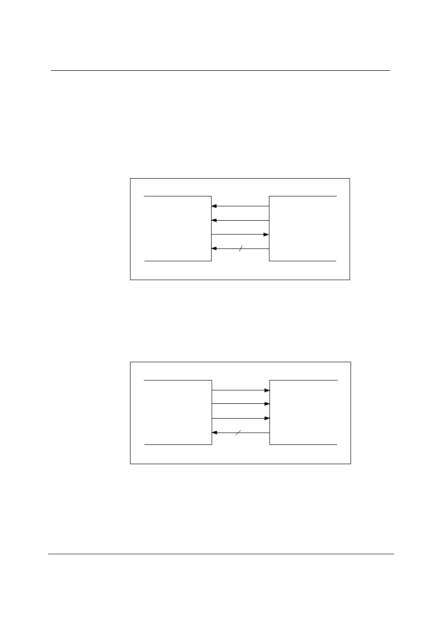
DIGITAL AUDIO INTERFACE ≠ MASTER MODE
LRC
DOUT
DIN1/2/3
WM8772
CODEC
DSP/
ENCODER/
DECODER
3
BCLK
Figure 14 Audio Interface - Master Mode
Production Data
WM8772EDS ≠ 28 PIN SSOP
w
PD Rev 4.1 October 2004
17
BCLK
(Output)
DOUT
LRC
(Output)
t
DL
DIN1/2/3
t
DDA
t
DHT
t
DST
Figure 15 Digital Audio Data Timing ≠ Master Mode
Test Conditions
AVDD, VREFP = 5V, DVDD = 3.3V, AGND, VREFN, DGND = 0V, T
A
= +25
o
C, Master Mode, fs = 48kHz, MCLK = 256fs unless
otherwise stated.
PARAMETER SYMBOL
TEST
CONDITIONS
MIN
TYP
MAX
UNIT
Audio Data Input Timing Information
LRC propagation delay from
BCLK falling edge
t
DL
0
10
ns
DOUT propagation delay
from BCLK falling edge
t
DDA
0
10
ns
DIN1/2/3 setup time to
BCLK rising edge
t
DST
10
ns
DIN1/2/3 hold time from
BCLK rising edge
t
DHT
10
ns
Table 3 Digital Audio Data Timing ≠ Master Mode

WM8772EDS ≠ 28 PIN SSOP
Production Data
w
PD Rev 4.1 October 2004
18
DIGITAL AUDIO INTERFACE ≠ SLAVE MODE
LRC
DOUT
BCLK
DIN1/2/3
WM8772
CODEC
DSP
ENCODER/
DECODER
3
Figure 16 Audio Interface ≠ Slave Mode
BCLK
LRC
t
BCH
t
BCL
t
BCY
DIN1/2/3
DOUT
t
LRSU
t
DS
t
LRH
t
DH
t
DD
Figure 17 Digital Audio Data Timing ≠ Slave Mode
Test Conditions
AVDD = 5V, DVDD = 3.3V, AGND = 0V, DGND = 0V, T
A
= +25
o
C, Slave Mode, fs = 48kHz, MCLK = 256fs unless otherwise
stated.
PARAMETER SYMBOL
TEST
CONDITIONS
MIN
TYP
MAX
UNIT
Audio Data Input Timing Information
BCLK cycle time
t
BCY
50
ns
BCLK pulse width high
t
BCH
20
ns
BCLK pulse width low
t
BCL
20
ns
LRC set-up time to BCLK
rising edge
t
LRSU
10
ns
LRC hold time from BCLK
rising edge
t
LRH
10
ns
DIN1/2/3 set-up time to
BCLK rising edge
t
DS
10
ns
DIN1/2/3 hold time from
BCLK rising edge
t
DH
10
ns

Production Data
WM8772EDS ≠ 28 PIN SSOP
w
PD Rev 4.1 October 2004
19
Test Conditions
AVDD = 5V, DVDD = 3.3V, AGND = 0V, DGND = 0V, T
A
= +25
o
C, Slave Mode, fs = 48kHz, MCLK = 256fs unless otherwise
stated.
PARAMETER SYMBOL
TEST
CONDITIONS
MIN
TYP
MAX
UNIT
DOUT propagation delay
from BCLK falling edge
t
DD
0
10
ns
Table 4 Digital Audio Data Timing ≠ Slave Mode
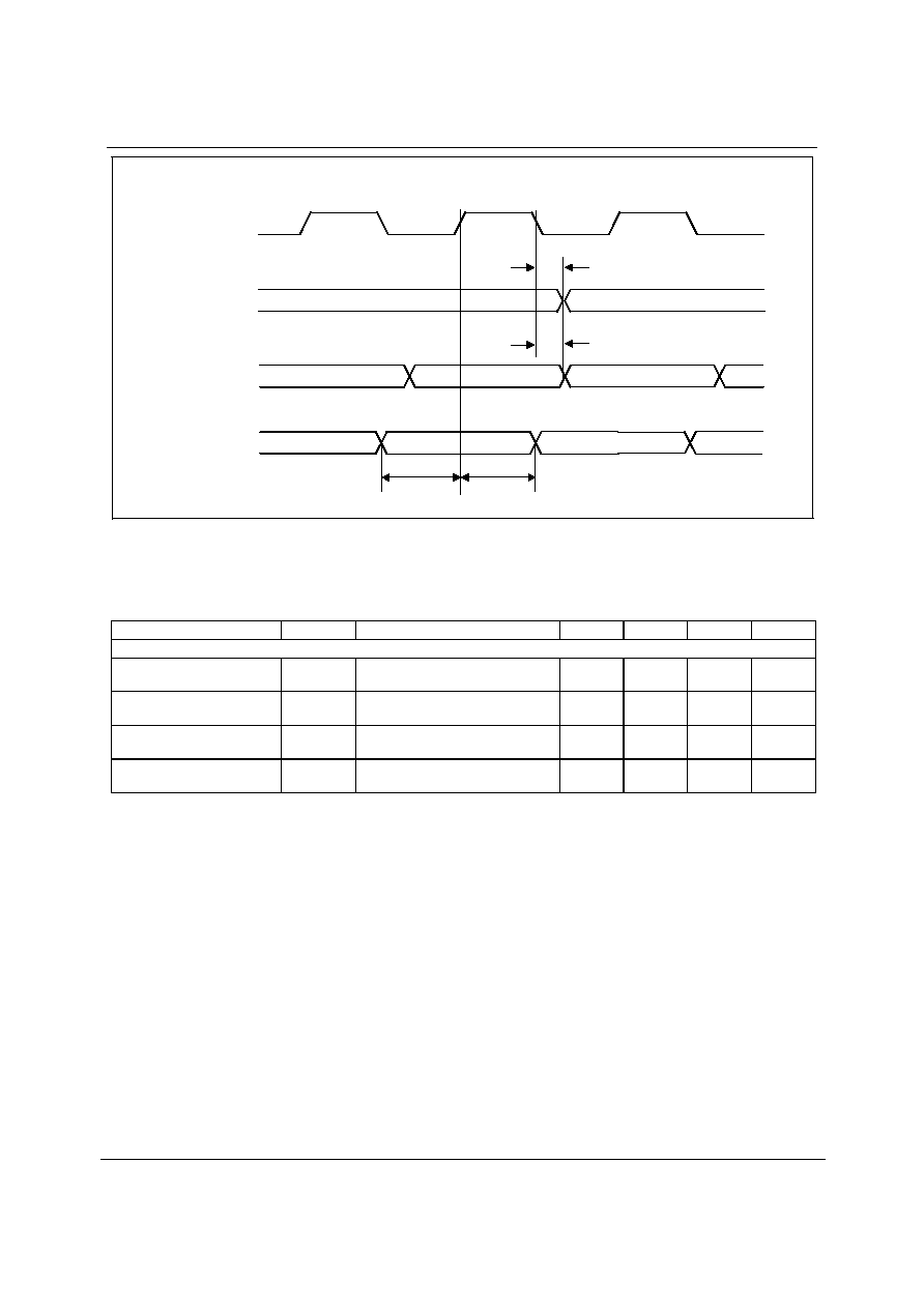
MPU INTERFACE TIMING
ML/I2S
MC/IWL
MD/DM
t
CSL
t
DHO
t
DSU
t
CSH
t
SCY
t
SCH
t
SCL
t
SCS
LSB
t
CSS
Figure 18 SPI Compatible Control Interface Input Timing
Test Conditions
AVDD = 5V, DVDD = 3.3V, AGND, DGND = 0V, T
A
= +25
o
C, fs = 48kHz, DACMCLK and ADCMCLK = 256fs unless otherwise
stated
PARAMETER SYMBOL
MIN
TYP
MAX
UNIT
MC/IWL rising edge to ML/I2S rising edge
t
SCS
60
ns
MC/IWL pulse cycle time
t
SCY
80
ns
MC/IWL pulse width low
t
SCL
30
ns
MC/IWL pulse width high
t
SCH
30
ns
MD/DM to MC/IWL set-up time
t
DSU
20
ns
MC/IWL to MD/DM hold time
t
DHO
20
ns
ML/I2S pulse width low
t
CSL
20
ns
ML/I2S pulse width high
t
CSH
20
ns
ML/I2S rising to MC/IWL rising
t
CSS
20
ns
Table 5 3-Wire SPI Compatible Control Interface Input Timing Information

WM8772EDS ≠ 28 PIN SSOP
Production Data
w
PD Rev 4.1 October 2004
20
DEVICE DESCRIPTION
INTRODUCTION
WM8772EDS is a complete 6-channel DAC, 2-channel ADC audio codec, including digital
interpolation and decimation filters, multi-bit sigma delta stereo ADC, and switched capacitor multi-
bit sigma delta DACs with digital volume controls on each channel and output smoothing filters.
The device is implemented as three separate stereo DACs and a stereo ADC in a single package
and controlled by a single interface.
Each stereo DAC has its own data input DIN1/2/3, the stereo ADC has it's own data output DOUT.
The word clock LRC, bit clock BCLK and master clock MCLK are shared between them.
The Audio Interface may be configured to operate in either master or slave mode. In Slave mode
LRC and BCLK are all inputs. In Master mode LRC and BCLK are all outputs.
Each DAC has its own digital volume control that is adjustable in 0.5dB steps. The digital volume
controls may be operated independently. In addition, a zero cross detect circuit is provided for each
DAC for the digital volume controls. The digital volume control detects a transition through the zero
point before updating the volume. This minimises audible clicks and `zipper' noise as the gain values
change.
Control of internal functionality of the device is by 3-wire serial or pin programmable control interface.
The software control interface may be asynchronous to the audio data interface as control data will
be re-synchronised to the audio processing internally.
Operation using master clocks of 128fs, 192fs, 256fs, 384fs, 512fs or 768fs is provided for the DAC,
for operation of both the ADC and DAC master clocks of 256fs, 384fs, 512fs and 768fs is provided.
In Slave mode selection between clock rates is automatically controlled. In master mode, the sample
rate is set by control bits RATE. Audio sample rates (fs) from less than 8ks/s up to 192ks/s are
allowed for the DAC and from less than 32ks/s up to 96ks/s for the ADC, provided the appropriate
master clock is input.
The audio data interface supports right, left and I
2
S interface formats along with a highly flexible DSP
serial port interface.
AUDIO DATA SAMPLING RATES
In a typical digital audio system there is only one central clock source producing a reference clock to
which all audio data processing is synchronised. This clock is often referred to as the audio system's
Master Clock. The external master system clock can be applied directly through the MCLK input pin
with no software configuration necessary. In a system where there are a number of possible sources
for the reference clock it is recommended that the clock source with the lowest jitter be used to
optimise the performance of the ADC and DAC.
The master clock for WM8772EDS supports audio sampling rates from 128fs to 768fs, where fs is
the audio sampling frequency (LRC) typically 32kHz, 44.1kHz, 48kHz, 96kHz or 192kHz (for DAC
operation only). For ADC operation sample rates from 256fs to 768fs are supported. The master
clock is used to operate the digital filters and the noise shaping circuits.
In Slave mode the WM8772EDS has a master clock detection circuit that automatically determines
the relationship between the system clock frequency and the sampling rate (to within +/- 32 master
clocks). If there is a greater than 32 clocks error the interface defaults to 768fs mode. The master
clocks must be synchronised with LRC, although the WM8772EDS is tolerant of phase variations or
jitter on this clock. Table 6 shows the typical master clock frequency inputs for the WM8772EDS.
The signal processing for the WM8772EDS typically operates at an oversampling rate of 128fs for
both ADC and DAC. The exception to this for the DAC is for operation with a 128/192fs system clock,
e.g. for 192kHz operation, when the oversampling rate is 64fs. For ADC operation at 96kHz it is
recommended that the user set the ADCOSR bit. This changes the ADC signal processing
oversample rate to 64fs.

Production Data
WM8772EDS ≠ 28 PIN SSOP
w
PD Rev 4.1 October 2004
21
System Clock Frequency (MHz)
SAMPLING
RATE
(LRC)
128fs 192fs 256fs 384fs 512fs 768fs
32kHz 4.096 6.144 8.192 12.288
16.384 24.576
44.1kHz 5.6448 8.467 11.2896
16.9340
22.5792 33.8688
48kHz 6.144 9.216 12.288
18.432
24.576 36.864
96kHz 12.288
18.432 24.576 36.864
Unavailable
Unavailable
192kHz 24.576 36.864
Unavailable
Unavailable
Unavailable
Unavailable
Table 6 System Clock Frequencies Versus Sampling Rate
(ADC does not support 128fs and 192fs)
HARDWARE CONTROL MODES
When the MODE pin is held high, the following hardware modes of operation are available.
Note: When in hardware mode the ADC and DAC will only run in slave mode.
MUTE AND AUTOMUTE OPERATION
In both hardware and software modes, MUTE controls the selection of MUTE directly, and can be
used to enable and disable the automute function. This pin becomes an output when left floating and
indicates infinite ZERO detect (IZD) has been detected.
DESCRIPTION
0
Normal Operation
1
Mute DAC channels
Floating
Enable IZD, MUTE becomes an output to indicate when IZD occurs.
L=IZD detected, H=IZD not detected.
Table 7 Mute and Automute Control
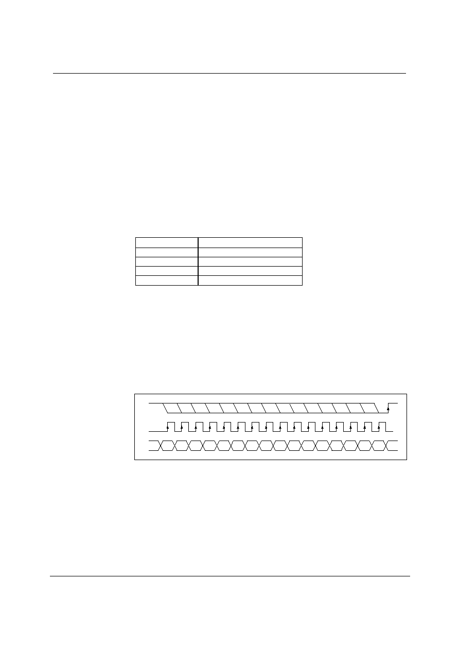
Figure 19 shows the application and release of MUTE whilst a full amplitude sinusoid is being played
at 48kHz sampling rate. When MUTE (lower trace) is asserted, the output (upper trace) begins to
decay exponentially from the DC level of the last input sample. The output will decay towards V
MID
with a time constant of approximately 64 input samples. If MUTE is applied to all channels for 1024
or more input samples the outputs will be connected directly to V
MID
if IZD is set. When MUTE is de-
asserted, the output will restart immediately from the current input sample.
Figure 19 Application and Release of Soft Mute
-2.5
-2
-1.5
-1
-0.5
0
0.5
1
1.5
0
0.001
0.002
0.003
0.004
0.005
0.006
Time(s)

WM8772EDS ≠ 28 PIN SSOP
Production Data
w
PD Rev 4.1 October 2004
22
The MUTE pin is an input to select mute or not mute. MUTE is active high; taking the pin high causes
the filters to soft mute, ramping down the audio signal over a few milliseconds. Taking MUTE low
again allows data into the filter.
The automute function detects a series of ZERO value audio samples of 1024 samples long being
applied to both channels. After such an event, a latch is set whose output (AUTOMUTED) is wire
OR'ed through a 10k resistor to the MUTE pin. Thus if the MUTE pin is not being driven, the
automute function will assert mute.
If MUTE is tied low, AUTOMUTED is overridden and will not mute unless the IZD register bit is set. If
MUTE is driven from a bi-directional source, then both MUTE and automute functions are available. If
MUTE is not driven, AUTOMUTED appears as a weak output (10k source impedance) and can be
used to drive external mute circuits. AUTOMUTED will be removed as soon as any channel receives
a non-ZERO input.
A diagram showing how the various Mute modes interact is shown below Figure 20.
IZD (Register Bit)
AUTOMUTED
(Internal Signal)
10k
MUTE (Register Bit)
SOFTMUTE
(Internal
Signal)
MUTE
PIN
Figure 20 Selection Logic for MUTE Modes
INPUT FORMAT SELECTION
In hardware mode, ML/I2S and MC/IWL become input controls for selection of input data format type
and input data word length for both the ADC and DAC.
ML/I2S MC/IWL
INPUT
DATA
MODE
0 0
24-bit right justified
0 1
20-bit right justified
1 0
16-bit I
2
S
1 1
24-bit I
2
S
Table 8 Input Format Selection
Note:
In 24 bit I
2
S mode, any width of 24 bits or less is supported provided that the left/right clocks (LRC)
are high for a minimum of 24 bit clocks (BCLK) and low for a minimum of 24 bit clocks.
DE-EMPHASIS CONTROL
In hardware mode, the MD/DM pin becomes an input control for selection of de-emphasis filtering to
be applied.
MD/DM DE-EMPHASIS
0 Off
1 On
Table 9 De-emphasis Control
Production Data
WM8772EDS ≠ 28 PIN SSOP
w
PD Rev 4.1 October 2004
23
DIGITAL AUDIO INTERFACE
MASTER AND SLAVE MODES
The audio interface operates in either Slave or Master mode, selectable using the MS control bit. In
both Master and Slave modes DIN1/2/3 are always inputs to the WM8772EDS and DOUT is always
an output. The default is Slave mode.
In Slave mode, LRC and BCLK are inputs to the WM8772EDS (Figure 21). DIN1/2/3 and LRC are
sampled by the WM8772EDS on the rising edge of BCLK. ADC data is output on DOUT and
changes on the falling edge of BCLK.
By setting the control bit BCP the polarity of BCLK may be reversed so that DIN1/2/3 and LRC are
sampled on the falling edge of BCLK and DOUT changes on the rising edge of BCLK.
LRC
DOUT
BCLK
DIN1/2/3
WM8772
CODEC
DSP
ENCODER/
DECODER
3
Figure 21 Slave Mode
In Master mode, LRC and BCLK are outputs from the WM8772EDS (Figure 22). LRC and BCLK are
generated by the WM8772EDS. DIN1/2/3 are sampled by the WM8772EDS on the rising edge of
BCLK so the controller must output DAC data that changes on the falling edge of BCLK. ADC data is
output on DOUT and changes on the falling edge of BCLK.
By setting control bit BCP the polarity of BCLK may be reversed so that DIN1/2/3 are sampled on the
falling edge of BCLK, and DOUT changes on the rising edge of BCLK.
DOUT
BCLK
DIN1/2/3
LRC
WM8772
CODEC
DSP/
ENCODER/
DECODER
3
Figure 22 Master Mode

WM8772EDS ≠ 28 PIN SSOP
Production Data
w
PD Rev 4.1 October 2004
24
AUDIO INTERFACE FORMATS
Audio data is applied to the internal DAC filters, or output from the ADC filters, via the Digital Audio
Interface. 5 popular interface formats are supported:
∑
Left Justified mode
∑
Right Justified mode
∑
I
2
S mode
∑
DSP
Early
mode
∑
DSP Late mode
All 5 formats send the MSB first and support word lengths of 16, 20, 24 and 32 bits, with the
exception of 32 bit right justified mode, which is not supported.
In left justified, right justified and I
2
S modes, the digital audio interface receives DAC data on the
DIN1/2/3 inputs and outputs ADC data on DOUT. Audio Data for each stereo channel is time
multiplexed with LRC indicating whether the left or right channel is present. LRC is also used as a
timing reference to indicate the beginning or end of the data words.
In left justified, right justified and I
2
S modes, the minimum number of BCLKs per LRC period is 2
times the selected word length. LRC must be high for a minimum of word length BCLKs and low for a
minimum of word length BCLKs. Any mark to space ratio on LRC is acceptable provided the above
requirements are met.
In DSP early or DSP late mode, all 6 DAC channels are time multiplexed onto DIN1. LRC is used as
a frame sync signal to identify the MSB of the first word. The minimum number of BCLKs per LRC
period is 6 times the selected word length. Any mark to space ratio is acceptable on LRC provided
the rising edge is correctly positioned. The ADC data may also be output in DSP early or late modes,
with LRC used as a frame sync to identify the MSB of the first word. The minimum number of BCLKs
per LRC period is 2 times the selected word length if only the ADC is being operated.
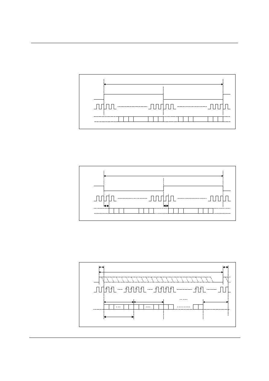
LEFT JUSTIFIED MODE
In left justified mode, the MSB of DIN1/2/3 is sampled by the WM8772EDS on the first rising edge of
BCLK following a LRC transition. The MSB of the ADC data is output on DOUT and changes on the
same falling edge of BCLK as LRC and may be sampled on the rising edge of BCLK. LRC is high
during the left samples and low during the right samples (Figure 23).
LEFT CHANNEL
RIGHT CHANNEL
DACLRC/
ADCLRC
DACBCLK/
ADCBCLK
DIN1/2/3/
DOUT
1/fs
n
3
2
1
n-2 n-1
LSB
MSB
n
3
2
1
n-2 n-1
LSB
MSB
Figure 23 Left Justified Mode Timing Diagram
Production Data
WM8772EDS ≠ 28 PIN SSOP
w
PD Rev 4.1 October 2004
25
RIGHT JUSTIFIED MODE
In right justified mode, the LSB of DIN1/2/3 is sampled by the WM8772EDS on the rising edge of
BCLK preceding a LRC transition. The LSB of the ADC data is output on DOUT and changes on the
falling edge of BCLK preceding a LRC transition and may be sampled on the rising edge of BCLK.
LRC are high during the left samples and low during the right samples (Figure 24).
LEFT CHANNEL
RIGHT CHANNEL
DACLRC/
ADCLRC
DACBCLK/
ADCBCLK
DIN1/2/3/
DOUT
1/fs
n
3
2
1
n-2 n-1
LSB
MSB
n
3
2
1
n-2 n-1
LSB
MSB
Figure 24 Right Justified Mode Timing Diagram
I
2
S MODE
In I
2
S mode, the MSB of DIN1/2/3 is sampled by the WM8772EDS on the second rising edge of
BCLK following a LRC transition. The MSB of the ADC data is output on DOUT and changes on the
first falling edge of BCLK following an LRC transition and may be sampled on the rising edge of
BCLK. LRC are low during the left samples and high during the right samples.
LEFT CHANNEL
RIGHT CHANNEL
DACLRC/
ADCLRC
DACBCLK/
ADCBCLK
DIN1/2/3/
DOUT
1/fs
n
3
2
1
n-2 n-1
LSB
MSB
n
3
2
1
n-2 n-1
LSB
MSB
1 BCLK
1 BCLK
Figure 25 I
2
S Mode Timing Diagram
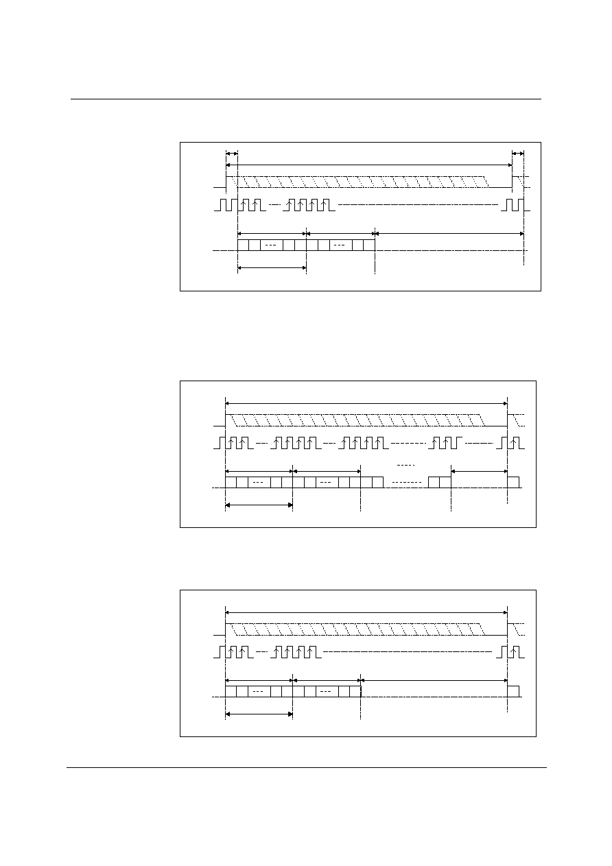
DSP EARLY MODE
In DSP early mode, the MSB of DAC channel 1 left data is sampled by the WM8772EDS on the
second rising edge on BCLK following a LRC rising edge. DAC channel 1 right and DAC channels 2
and 3 data follow DAC channel 1 left data (Figure 26).
DACLRC
DACBCLK
DIN1
Input Word Length (IWL)
1/fs
CHANNEL 1
LEFT
n
2
1
n-1
LSB
MSB
n
2
1
n-1
CHANNEL 1
RIGHT
2
1
CHANNEL 2
LEFT
n
n-1
CHANNEL 3
RIGHT
NO VALID DATA
1 BCLK
1 BCLK
Figure 26 DSP Early Mode Timing Diagram ≠ DAC Data Input
WM8772EDS ≠ 28 PIN SSOP
Production Data
w
PD Rev 4.1 October 2004
26
The MSB of the left channel ADC data is output on DOUT and changes on the first falling edge of
BCLK following a low to high LRC transition and may be sampled on the rising edge of BCLK. The
right channel ADC data is contiguous with the left channel data (Figure 27)
ADCLRC
ADCBCLK
DOUT
Input Word Length (IWL)
1/fs
LEFT CHANNEL
n
2
1
n-1
LSB
MSB
n
2
1
n-1
RIGHT CHANNEL
NO VALID DATA
1 BCLK
1 BCLK
Figure 27 DSP Early Mode Timing Diagram ≠ ADC Data Output
DSP LATE MODE
In DSP late mode, the MSB of DAC channel 1 left data is sampled by the WM8772EDS on the first
BCLK rising edge following a LRC rising edge. DAC channel 1 right and DAC channels 2 and 3 data
follow DAC channel 1 left data (Figure 28).
DACLRC
DACBCLK
DIN1
Input Word Length (IWL)
1/fs
CHANNEL 1
LEFT
n
2
1
n-1
LSB
MSB
n
2
1
n-1
CHANNEL 1
RIGHT
2
1
CHANNEL 2
LEFT
n
n-1
CHANNEL 3
RIGHT
NO VALID DATA
1
Figure 28 DSP Late Mode Timing Diagram ≠ DAC Data Input
The MSB of the left channel ADC data is output on DOUT and changes on the same falling edge of
BCLK as the low to high LRC transition and may be sampled on the rising edge of BCLK. The right
channel ADC data is contiguous with the left channel data (Figure 29).
ADCLRC
BCK
DOUT
Input Word Length (IWL)
1/fs
LEFT CHANNEL
n
2
1
n-1
LSB
MSB
n
2
1
n-1
RIGHT CHANNEL
NO VALID DATA
1
Figure 29 DSP Late Mode Timing Diagram ≠ ADC Data Output
Production Data
WM8772EDS ≠ 28 PIN SSOP
w
PD Rev 4.1 October 2004
27
In both early and late DSP modes, DACL1 is always sent first, followed immediately by DACR1 and
the data words for the other 6 channels. No BCLK edges are allowed between the data words. The
word order is DAC1 left, DAC1 right, DAC2 left, DAC2 right, DAC3 left, DAC3 right.
POWERDOWN MODES
The WM8772EDS has powerdown control bits allowing specific parts of the WM8772EDS to be
powered off when not being used. Control bit ADCPD powers off the ADC. The three stereo DACs
each have a separate powerdown control bit, DACPD[2:0] allowing individual stereo DACs to be
powered off when not in use. Setting ADCPD and DACPD[2:0] will powerdown everything except the
references VMID and REFADC. These may be powered down by setting PDWN. Setting PDWN will
override all other powerdown control bits. It is recommended that the ADC and DACs are powered
down before setting PDWN.
ZERO DETECT
The WM8772EDS has a zero detect circuit for each DAC channel that detects when 1024
consecutive zero samples have been input. The MUTE pin output may be programmed to output the
zero detect signal (see Table 10) which may then be used to control external muting circuits. A `1' on
MUTE indicates a zero detect. The zero detect may also be used to automatically enable DAC mute
by setting IZD.
DZFM[1:0] MUTE
00 All
channels
zero
01 Channel
1
zero
10 Channel
2
zero
11 Channel
3
zero
Table 10 Zero Flag Output Select
SOFTWARE CONTROL INTERFACE OPERATION
The WM8772EDS is controlled using a 3-wire serial interface in software mode or pin
programmable in hardware mode.
The control mode is selected by the state of the MODE pin.
3-WIRE (SPI COMPATIBLE) SERIAL CONTROL MODE
MD/DM is used for the program data, MC/IWL is used to clock in the program data and ML/I2S is
used to latch the program data. MD/DM is sampled on the rising edge of MC/IWL. The 3-wire
interface protocol is shown in Figure 30.
B15 B14 B13 B12 B11 B10 B9 B8 B7 B6 B5 B4 B3 B2 B1 B0
ML/I2S
MC/IWL
MD/DM
Figure 30 3-Wire SPI Compatible Interface
1.
B[15:9] are Control Address Bits
2.
B[8:0] are Control Data Bits
3.
ML/I2S is edge sensitive ≠ the data is latched on the rising edge of ML/I2S.
WM8772EDS ≠ 28 PIN SSOP
Production Data
w
PD Rev 4.1 October 2004
28
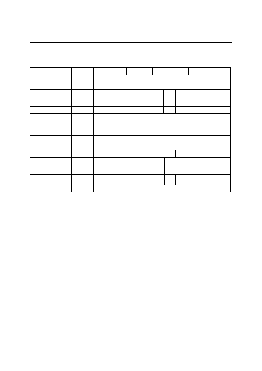
REGISTER MAP - 28 PIN SSOP
The complete register map is shown below. The detailed description can be found in the relevant text of the device description. The
WM8772EDS can be configured using the Control Interface. All unused bits should be set to `0'.
REGISTER
B15
B14
B13
B12
B11
B10
B9
B8
B7
B6
B5
B4
B3
B2
B1
B0
DEFAULT
R0(00h)
0
0
0
0
0
0
0
UPDATE LDA1[7:0] 011111111
R1(01h)
0
0
0
0
0
0
1
UPDATE RDA1[7:0] 011111111
R2(02h)
0
0
0
0
0
1
0
PL[8:5]
IZD ATC
PDWN
All DAC
DEEMP
MUTE
All DAC
100100000
R3(03h)
0
0
0
0
0
1
1
PHASE[8:6]
IWL[5:4] BCP
LRP FMT[1:0]
000000000
R4(04h)
0
0
0
0
1
0
0
UPDATE LDA2[7:0] 011111111
R5(05h)
0
0
0
0
1
0
1
UPDATE RDA2[7:0] 011111111
R6(06h)
0
0
0
0
1
1
0
UPDATE LDA3[7:0] 011111111
R7(07h)
0
0
0
0
1
1
1
UPDATE RDA3[7:0] 011111111
R8(08h)
0
0
0
1
0
0
0
UPDATE MASTDA[7:0] 011111111
R9(09h)
0
0
0
1
0
0
1
DEEMP[8:6]
DMUTE[5:3] DZFM[2:1]
ZCD
000000000
R10(0Ah)
0
0
0
1
0
1
0
RATE[8:6]
MS PWRDNALL
DACPD[3:1]
ADCPD
010000000
R11(0Bh)
0
0
0
1
0
1
1
ADC
OSR
010 0
00
00
001000000
R12(0Ch)
0
0
0
1
1
0
0
0 0
MPD
0 0
ADCHP
AMUTE
ALL
AMUTEL AMUTER 000000000
R31(1Fh)
0
0
1
1
1
1
1
RESET
000000000
Production Data
WM8772EDS ≠ 28 PIN SSOP
w
PD Rev 4.1 October 2004
29
CONTROL INTERFACE REGISTERS
ATTENUATOR CONTROL MODE
Setting the ATC register bit causes the left channel attenuation settings to be applied to both left and
right channel DACs from the next audio input sample. No update to the attenuation registers is
required for ATC to take effect.
REGISTER ADDRESS
BIT
LABEL
DEFAULT
DESCRIPTION
0000010
DAC Channel Control
3 ATC
0
Attenuator Control Mode:
0: Right channels use right
attenuations
1: Right channels use left
attenuations
INFINITE ZERO DETECT ENABLE
Setting the IZD register bit will enable the internal infinite zero detect function:
REGISTER ADDRESS
BIT
LABEL
DEFAULT
DESCRIPTION
0000010
DAC Channel Control
4 IZD
0 Infinite Zero Mute Enable
0 : Disable inifinite zero mute
1: Enable infinite zero mute
With IZD enabled, applying 1024 consecutive zero input samples each stereo channel will cause that
stereo channel outputs to be muted to V
MID
. Mute will be removed as soon as that stereo channel
receives a non-zero input.
DAC OUTPUT CONTROL
The DAC output control word determines how the left and right inputs to the audio Interface are
applied to the left and right DACs:
REGISTER ADDRESS
BIT
LABEL
DEFAULT
DESCRIPTION
PL[3:0] Left
Output
Right
Output
0000 Mute Mute
0001 Left Mute
0010 Right Mute
0011 (L+R)/2
Mute
0100 Mute Left
0101 Left Left
0110 Right Left
0111 (L+R)/2
Left
1000 Mute Right
1001 Left Right
1010 Right Right
1011 (L+R)/2
Right
1100 Mute (L+R)/2
1101 Left (L+R)/2
1110 Right (L+R)/2
0000010
DAC Control
8:5 PL[3:0]
1001
1111 (L+R)/2
(L+R)/2
WM8772EDS ≠ 28 PIN SSOP
Production Data
w
PD Rev 4.1 October 2004
30
ADC AND DAC DIGITAL AUDIO INTERFACE CONTROL REGISTER
Interface format is selected via the FMT[1:0] register bits:
REGISTER ADDRESS
BIT
LABEL
DEFAULT
DESCRIPTION
0000011
Interface Control
1:0 FMT
[1:0]
00
Interface Format Select:
00 : Right justified mode
01: Left justified mode
10:
I
2
S mode
11: DSP (early or late) mode
In left justified, right justified or I
2
S modes, the LRP register bit controls the polarity of LRC. If this bit
is set high, the expected polarity of LRC will be the opposite of that shown Figure 23, Figure 24 and
Figure 25. Note that if this feature is used as a means of swapping the left and right channels, a 1
sample phase difference will be introduced. In DSP modes, the LRP register bit is used to select
between early and late modes.
REGISTER ADDRESS
BIT
LABEL
DEFAULT
DESCRIPTION
In left/right/I
2
S Modes:
LRC Polarity (normal)
0 : Normal LRC polarity
1: Inverted LRC polarity
0000011
Interface Control
2 LRP
0
In DSP Mode:
0 : Early DSP mode
1: Late DSP mode
By default, LRC and DIN1/2/3 are sampled on the rising edge of BCLK and should ideally change on
the falling edge. By default, LRC and DOUT are sampled on the rising edge of BCLK and should
ideally change on the falling edge. Data sources that change LRC and DOUT on the rising edge of
BCLK can be supported by setting the BCP register bit. Data sources that change LRC and DIN1/2/3
on the rising edge of BCLK can be supported by setting the BCP register bit. Setting BCP to 1
inverts the polarity of BCLK to the inverse of that shown in Figure 23, Figure 24, Figure 25, Figure
26, Figure 27, Figure 28 and Figure 29.
REGISTER ADDRESS
BIT
LABEL
DEFAULT
DESCRIPTION
0000011
Interface Control
3 BCP
0
BCLK Polarity (DSP Modes):
0: Normal BCLK polarity
1: Inverted BCLK polarity
The IWL[1:0] bits are used to control the input word length.
REGISTER ADDRESS
BIT
LABEL
DEFAULT
DESCRIPTION
0000011
Interface Control
5:4 IWL
[1:0]
00
Input Word Length:
00 : 16 bit data
01: 20 bit data
10: 24 bit data
11: 32 bit data
Note: 32-bit right justified mode is not supported.
In all modes, the data is signed 2's complement. The digital filters always input 24-bit data. If the
DAC is programmed to receive 16 or 20 bit data, the WM8772EDS pads the unused LSBs with
zeros. If the DAC is programmed into 32 bit mode, the 8 LSBs are ignored.
Note: In 24 bit I
2
S mode, any width of 24 bits or less is supported provided that LRC is high for a
minimum of 24 BCLKs and low for a minimum of 24 BCLKs.
A number of options are available to control how data from the Digital Audio Interface is applied to
the DAC channels.
Production Data
WM8772EDS ≠ 28 PIN SSOP
w
PD Rev 4.1 October 2004
31
DAC OUTPUT PHASE
The DAC Phase control word determines whether the output of each DAC is non-inverted or inverted
REGISTER ADDRESS
BIT
LABEL
DEFAULT
DESCRIPTION
Bit DAC
Phase
0 DAC1L/R
1
=
invert
1 DAC2L/R
1
=
invert
0000011
DAC Phase
8:6 PHASE
[2:0]
000
2 DAC3L/R
1
=
invert
DIGITAL ZERO CROSS-DETECT
The Digital volume control also incorporates a zero cross detect circuit which detects a transition
through the zero point before updating the digital volume control with the new volume. This is
enabled by control bit DZCEN.
REGISTER ADDRESS
BIT
LABEL
DEFAULT
DESCRIPTION
0001001
DAC Control
0 ZCD
0 DAC Digital Volume Zero Cross
Disable:
0: Zero cross detect enabled
1: Zero cross detect disabled
MUTE FLAG OUTPUT
The DZFM control bits allow the selection of the six DAC channel zero flag bits for output on the
MUTEB pin. A `1' on MUTE indicates 1024 consecutive zero input samples to the DAC channels
selected.
REGISTER ADDRESS
BIT
LABEL
DEFAULT
DESCRIPTION
0001001
Zero Flag
2:1 DZFM[1:0]
00
Selects the output MUTE pin (A `1'
indicates 1024 consecutive zero
input samples on the DAC channels
selected.
00: All channels zero
01: Channel 1 zero
10: Channel 2 zero
11: Channel 3 zero
DAC MUTE MODES
The WM8772EDS has individual mutes for each of the three DAC channels. Setting MUTE for a
channel will apply a `soft' mute to the input of the digital filters of the channel muted.
REGISTER ADDRESS
BIT
LABEL
DEFAULT
DESCRIPTION
0001001
DAC Mute
5:3 DMUTE
[2:0]
000
DAC Soft Mute Select
DMUTE [2:0]
DAC CHANNEL 1
DAC CHANNEL 2
DAC CHANNEL 3
000
Not MUTE
Not MUTE
Not MUTE
001 MUTE
Not
MUTE
Not
MUTE
010 Not
MUTE
MUTE
Not
MUTE
011 MUTE
MUTE
Not
MUTE
100
Not MUTE
Not MUTE
MUTE
101 MUTE
Not
MUTE
MUTE
110 Not
MUTE
MUTE MUTE

WM8772EDS ≠ 28 PIN SSOP
Production Data
w
PD Rev 4.1 October 2004
32
Setting the MUTEALL register bit will apply a 'soft' mute to the input of all the DAC digital filters:
REGISTER ADDRESS
BIT
LABEL
DEFAULT
DESCRIPTION
0000010
DAC Mute
0 MUTEALL
0
Soft Mute Select:
0 : Normal operation
1: Soft mute all channels
Refer to Figure 19 for the plot of application and release of soft mute.
Note that all other means of muting the DAC channels: setting the PL[3:0] bits to 0, setting the
PDWN bit or setting attenuation to 0 will cause much more abrupt muting of the output.
ADC MUTE MODES
Each ADC channel also has a mute control bit, which mutes the inputs to the ADC.
REGISTER ADDRESS
BIT
LABEL
DEFAULT
DESCRIPTION
0 AMUTER
0
ADC Mute Select:
0 : Normal operation
1: mute ADC right
1 AMUTEL
0 ADC Mute Select:
0 : Normal operation
1: mute ADC left
0001100
ADC Mute
2 AMUTEALL
0
ADC Mute Select:
0 : Normal operation
1: mute both ADC channels
DE-EMPHASIS MODE
Each stereo DAC channel has an individual de-emphasis control bit:
REGISTER ADDRESS
BIT
LABEL
DEFAULT
DESCRIPTION
0001001
DAC De-Emphahsis
Control
[8:6]
DEEMPH
[1:0]
000
De-emphasis Channel Selection
Select:
DEEMPH
[1:0]
DAC CHANNEL 1
DAC CHANNEL 2
DAC CHANNEL 3
000
Not DE-EMPHASIS
Not DE-EMPHASIS
Not DE-EMPHASIS
001
DE-EMPHASIS
Not DE-EMPHASIS
Not DE-EMPHASIS
010 Not
DE-EMPHASIS
DE-EMPHASIS
Not
DE-EMPHASIS
011 DE-EMPHASIS
DE-EMPHASIS
Not
DE-EMPHASIS
100 Not
DE-EMPHASIS
Not
DE-EMPHASIS
DE-EMPHASIS
101 DE-EMPHASIS
Not
DE-EMPHASIS
DE-EMPHASIS
110 Not
DE-EMPHASIS
DE-EMPHASIS
DE-EMPHASIS
Refer to Figure 7, Figure 8, Figure 9, Figure 10, Figure 11 and Figure 12 for details of the De-
Emphasis performance at different sample rates.
REGISTER ADDRESS
BIT
LABEL
DEFAULT
DESCRIPTION
0000010
DAC DEMP
1 DEEMP
ALL
0
DEMMP Select:
0 : Normal operation
1: De-emphasis all channels
Production Data
WM8772EDS ≠ 28 PIN SSOP
w
PD Rev 4.1 October 2004
33
POWERDOWN MODE AND ADC/DAC DISABLE
Setting the PDWN register bit immediately powers down the DAC's on the WM8772EDS, overriding
the DACD powerdown bits control bits. All trace of the previous input samples are removed, but all
control register settings are preserved. When PDWN is cleared the digital filters will be reinitialised
REGISTER ADDRESS
BIT
LABEL
DEFAULT
DESCRIPTION
0000010
Powerdown Control
2 PDWN
0 Power Down all DAC's Select:
0: All DAC's enabled
1: All DAC's disabled
The ADC and DACs may also be powered down individually by setting the ADCPD and DACPD
disable bits. Setting ADCD will disable the ADC and select a low power mode. The ADC digital filters
will be reset and will reinitialise when ADCPD is unset. Each Stereo DAC channel has a separate
disable DACPD[2:0]. Setting DACPD for a channel will disable the DACs and select a low power
mode.
REGISTER ADDRESS
BIT
LABEL
DEFAULT
DESCRIPTION
0 ADCPD
0 ADC Disable:
0:
Active
1:
Disable
0001010
Powerdown Control
3:1 DACPD[2:0]
000
DAC Disable
DACPD [2:0]
DAC CHANNEL 1
DAC CHANNEL 2
DAC CHANNEL 3
000 Active Active Active
001 DISABLE Active Active
010 Active
DISABLE
Active
011 DISABLE DISABLE Active
100 Active
Active
DISABLE
101 DISABLE Active DISABLE
110 Active
DISABLE
DISABLE
111 DISABLE DISABLE DISABLE
MASTER POWERDOWN
This control bit powers down the references for the whole chop. Therefore for complete powerdown,
both the ADC and DACs should be powered down first before setting this bit.
REGISTER ADDRESS
BIT
LABEL
DEFAULT
DESCRIPTION
0001010
Interface Control
4 PWRDNALL
0
Master Power Down Bit:
0: Not powered down
1: Powered down
MASTER MODE SELECT
Control bit MS selects between audio interface Master and Slave Modes. In Master mode LRC and
BCLK are outputs and are generated by the WM8772EDS. In Slave mode LRC and BCLK are inputs
to WM8772EDS.
REGISTER ADDRESS
BIT
LABEL
DEFAULT
DESCRIPTION
0001010
Interface Control
5 MS
0 DAC Audio Interface Master/Slave
Mode Select:
0: Slave mode
1: Master mode
WM8772EDS ≠ 28 PIN SSOP
Production Data
w
PD Rev 4.1 October 2004
34
MASTER MODE LRC FREQUENCY SELECT
In Master mode the WM8772EDS generates LRC and BCLK. These clocks are derived from the
master clock and the ratio of MCLK to LRC is set by RATE.
REGISTER ADDRESS
BIT
LABEL
DEFAULT
DESCRIPTION
0001010
Interface Control
8:6 RATE
[2:0]
010
Master Mode
MCLK:LRC Ratio Select:
000: 128fs (DAC only)
001: 192fs (DAC only)
010:
256fs
011:
384fs
100:
512fs
101:
768fs
ADC OVERSAMPLING RATE SELECT
For ADC operation at 96kHz it is recommended that the user set the ADCOSR bit. This changes the
ADC signal processing oversample rate to 64fs. The 64fs oversampling rate is only available in
modes were a 96KHz rate is supported, i.e. 256fs or 384fs. In all other modes the ADC will stay in a
128fs oversampling rate irrespective of what this bit is set to.
REGISTER ADDRESS
BIT
LABEL
DEFAULT DESCRIPTION
0001011
ADC Oversampling Rate
8 ADCOSR
0
ADC Oversampling Rate Select:
0:
128x
oversampling
1:
64x
oversampling
ADC HIGHPASS FILTER DISABLE
The ADC digital filters contain a digital highpass filter. This defaults to enabled and can be disabled
using software control bit ADCHPD.
REGISTER ADDRESS
BIT
LABEL
DEFAULT
DESCRIPTION
0001100
ADC Control
3 ADCHPD
0
ADC Highpass Filter Disable:
0: Highpass filter enabled
1: Highpass filter disabled
MUTE PIN DECODE
The MUTE pin can either be used an output or an input. When used as an input the MUTE pins
action can controlled by setting the DZFM bit to select the corresponding DAC for applying the MUTE
to. As an output its meaning is selected by the DZFM control bits. By default selecting the MUTE to
represent if DAC1 has received more than 1024 midrail samples will cause the MUTE to be asserted
a softmute on DAC1. Disabling the decode block will cause any logical high on the MUTE pin to
apply a softmute to all DAC's.
REGISTER ADDRESS
BIT
LABEL
DEFAULT
DESCRIPTION
0001100
ADC Control
6 MPD
0 MUTE Pin Decode Disable:
0: MUTE pin decode enable
1: MUTE pin decode disable

Production Data
WM8772EDS ≠ 28 PIN SSOP
w
PD Rev 4.1 October 2004
35
DAC DIGITAL VOLUME CONTROL
The DAC volume may also be adjusted in the digital domain using independent digital attenuation
control registers
REGISTER
ADDRESS
BIT LABEL DEFAULT
DESCRIPTION
7:0
LDA1[7:0] 11111111
(0dB)
Digital Attenuation data for Left channel DACL1 in 0.5dB steps. See
Table 11
0000000
Digital
Attenuation
DACL1
8
UPDATE Not
latched Controls simultaneous update of all Attenuation Latches
0: Store LDA1 in intermediate latch (no change to output)
1: Store LDA1 and update attenuation on all channels
7:0
RDA1[6:0] 11111111
(0dB)
Digital Attenuation data for Right channel DACR1 in 0.5dB steps.
See Table 11
0000001
Digital
Attenuation
DACR1
8
UPDATE Not
latched Controls simultaneous update of all Attenuation Latches
0: Store RDA1 in intermediate latch (no change to output)
1: Store RDA1 and update attenuation on all channels.
7:0
LDA2[7:0] 11111111
(0dB)
Digital Attenuation data for Left channel DACL2 in 0.5dB steps. See
Table 11
0000100
Digital
Attenuation
DACL2
8
UPDATE Not
latched Controls simultaneous update of all Attenuation Latches
0: Store LDA2 in intermediate latch (no change to output)
1: Store LDA2 and update attenuation on all channels.
7:0
RDA2[7:0] 11111111
(0dB)
Digital Attenuation data for Right channel DACR2 in 0.5dB steps.
See Table 11
0000101
Digital
Attenuation
DACR2
8
UPDATE Not
latched Controls simultaneous update of all Attenuation Latches
0: Store RDA2 in intermediate latch (no change to output)
1: Store RDA2 and update attenuation on all channels.
7:0
LDA3[7:0] 11111111
(0dB)
Digital Attenuation data for Left channel DACL3 in 0.5dB steps. See
Table 11
0000110
Digital
Attenuation
DACL3
8
UPDATE Not
latched Controls simultaneous update of all Attenuation Latches
0: Store LDA3 in intermediate latch (no change to output)
1: Store LDA3 and update attenuation on all channels.
7:0
RDA3[7:0] 11111111
(0dB)
Digital Attenuation data for Right channel DACR3 in 0.5dB steps.
See Table 11
0000111
Digital
Attenuation
DACR3
8
UPDATE Not
latched Controls simultaneous update of all Attenuation Latches
0: Store RDA3 in intermediate latch (no change to output)
1: Store RDA3 and update attenuation on all channels.
7:0
MASTDA
[7:0]
11111111
(0dB)
Digital Attenuation data for all DAC channels in 0.5dB steps. See
Table 11
0001000
Master
Digital
Attenuation
(all channels)
8
UPDATE Not
latched Controls simultaneous update of all Attenuation Latches
0: Store gain in intermediate latch (no change to output)
1: Store gain and update attenuation on all channels.
L/RDAX[7:0] ATTENUATION
LEVEL
00(hex) -
dB (mute)
01(hex) -127dB
: :
: :
: :
FE(hex) -0.5dB
FF(hex) 0dB
Table 11 Digital Volume Control Attenuation Levels

WM8772EDS ≠ 28 PIN SSOP
Production Data
w
PD Rev 4.1 October 2004
36
SOFTWARE REGISTER RESET
Writing to register 11111 will cause a register reset, resetting all register bits to their default values.
The device will be held in this reset state until a subsequent register write to any address is
completed.
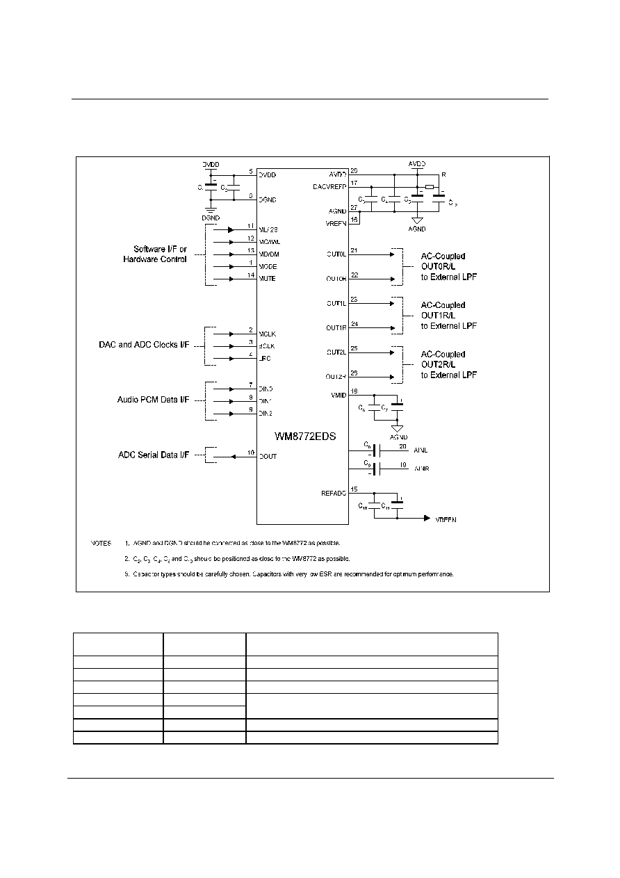
Production Data
WM8772EDS ≠ 28 PIN SSOP
w
PD Rev 4.1 October 2004
37
APPLICATIONS INFORMATION
RECOMMENDED EXTERNAL COMPONENTS
RECOMMENDED EXTERNAL COMPONENTS VALUES
COMPONENT
REFERENCE
SUGGESTED
VALUE
DESCRIPTION
C1 and C5
10
µ
F
De-coupling for DVDD and AVDD.
C2 to C4
0.1
µ
F
De-coupling for DVDD and AVDD.
C8 and C9
1
µ
F
Analogue input high pass filter capacitors
C6 and C10
0.1
µ
F
C7 and C11
10
µ
F
Reference de-coupling capacitors for VMID and ADCREF pin.
C12 10
µ
F
Filtering for VREFP. Omit if AVDD low noise.
R1 330
Filtering for VREP. Use 0
if AVDD low noise.
Table 12 External Components Description
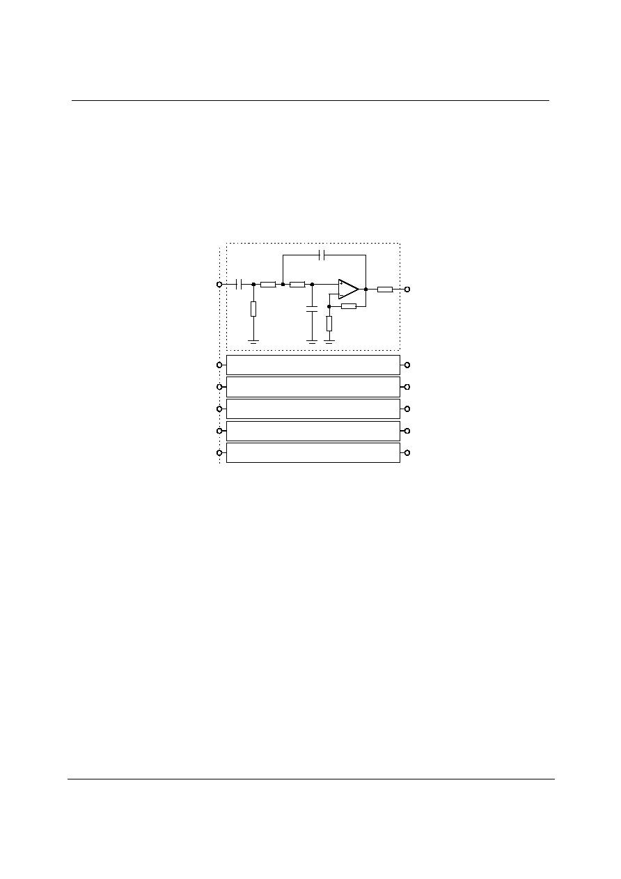
WM8772EDS ≠ 28 PIN SSOP
Production Data
w
PD Rev 4.1 October 2004
38
SUGGESTED ANALOGUE LOW PASS POST DAC FILTERS
It is recommended that a lowpass filter be applied to the output from each DAC channel for Hi Fi applications. Typically a
second order filter is suitable and provides sufficient attenuation of high frequency components (the unique low order, high
bit count multi-bit sigma delta DAC structure used in WM8772EDS produces much less high frequency output noise than
normal sigma delta DACs. This filter is typically also used to provide the 2x gain needed to provide the standard 2Vrms
output level from most consumer equipment.
Figure 31 shows a suitable post DAC filter circuit, with 2x gain. Alternative inverting filter architectures might also be used
with as good results.
7.5k
1.8k
10uF
1.0nF
10k
4.7k
680pF
4.7k
51
OP_FIL
VOUT1L
OP_FIL
VOUT1R
OP_FIL
VOUT2R
OP_FIL
VOUT2L
OP_FIL
VOUT3L
OP_FIL
VOUT3R
Figure 31 Recommended Post DAC Filter Circuit
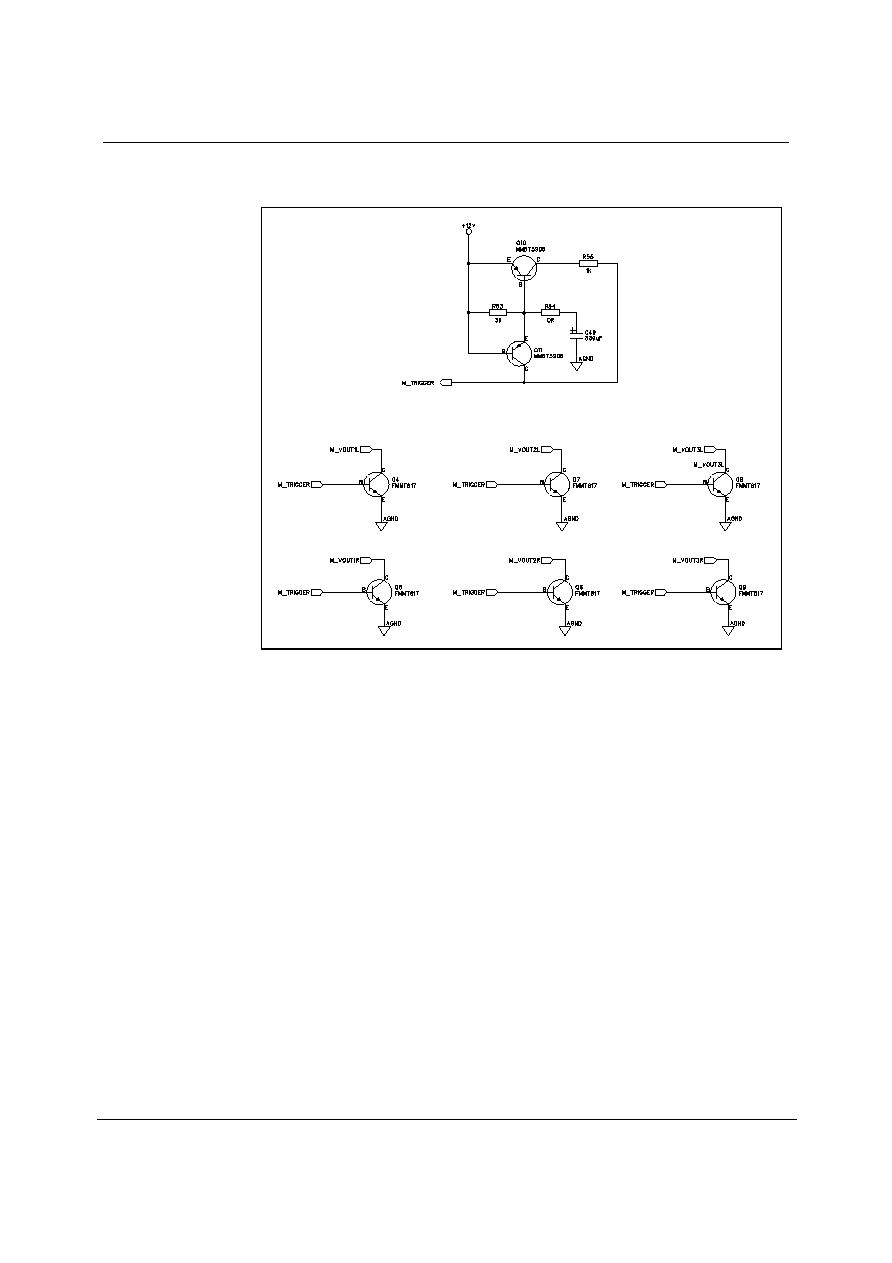
Production Data
WM8772EDS ≠ 28 PIN SSOP
w
PD Rev 4.1 October 2004
39
To ensure that system `pop' noise is kept to a minimum when power is applied or removed, a
transistor clamp circuit arrangement may be added to the output connectors of the system. A
recommended clamp circuit configuration is shown below.
Figure 32 Output Clamp Circuit
When the +VS power supply is applied, PNP transistor Q10 of the trigger circuit is held on until
capacitor C49 is fully charged. With transistor Q10 held `on', NPN transistors Q4 to Q9 of the clamp
circuits are also switched on holding the system outputs near to GND. When capacitor C49 is fully
charged transistors Q10 and Q4 to Q9 are switched off setting the outputs active.
When the +VS power supply is removed, PNP transistor Q11 of the trigger circuit is switched on. In
turn, transistors Q4 to Q9 of the clamp circuits are switched on holding the outputs of the evaluation
board near to GND until the rest of the circuitry on the board has settled.
Note: It is recommended that low Vce
sat
switching transistors should be used in this circuit to ensure
that the clamp is applied before the rest of the circuitry has time to power down.
Important: If a trigger circuit such as the one shown is to be used, it is important that the +VS
supply drops quicker than any other supply to ensure that the outputs are clamped during the
period when `pop' noise may occur.

WM8772EDS ≠ 28 PIN SSOP
Production Data
w
PD Rev 4.1 October 2004
40
PACKAGE DIMENSIONS
NOTES:
A. ALL LINEAR DIMENSIONS ARE IN MILLIMETERS.
B. THIS DRAWING IS SUBJECT TO CHANGE WITHOUT NOTICE.
C. BODY DIMENSIONS DO NOT INCLUDE MOLD FLASH OR PROTRUSION, NOT TO EXCEED 0.20MM.
D. MEETS JEDEC.95 MO-150, VARIATION = AH. REFER TO THIS SPECIFICATION FOR FURTHER DETAILS.
DM007.D
DS: 28 PIN SSOP (10.2 x 5.3 x 1.75 mm)
Symbols
Dimensions
(mm)
MIN
NOM
MAX
A
-----
-----
2.0
A
1
0.05
-----
0.25
A
2
1.65
1.75
1.85
b
0.22
0.30
0.38
c
0.09
-----
0.25
D
9.90
10.20
10.50
e
E
7.40
7.80
8.20
5.00
5.30
5.60
L
0.55
0.75
0.95
A A2
A1
14
1
15
28
E1
E
c
L
GAUGE
PLANE
0.25
e
b
D
SEATING PLANE
-C-
0.10 C
REF:
JEDEC.95, MO-150
E
1
L
1
0.125 REF
0.65 BSC
L
1
0
o
4
o
8
o
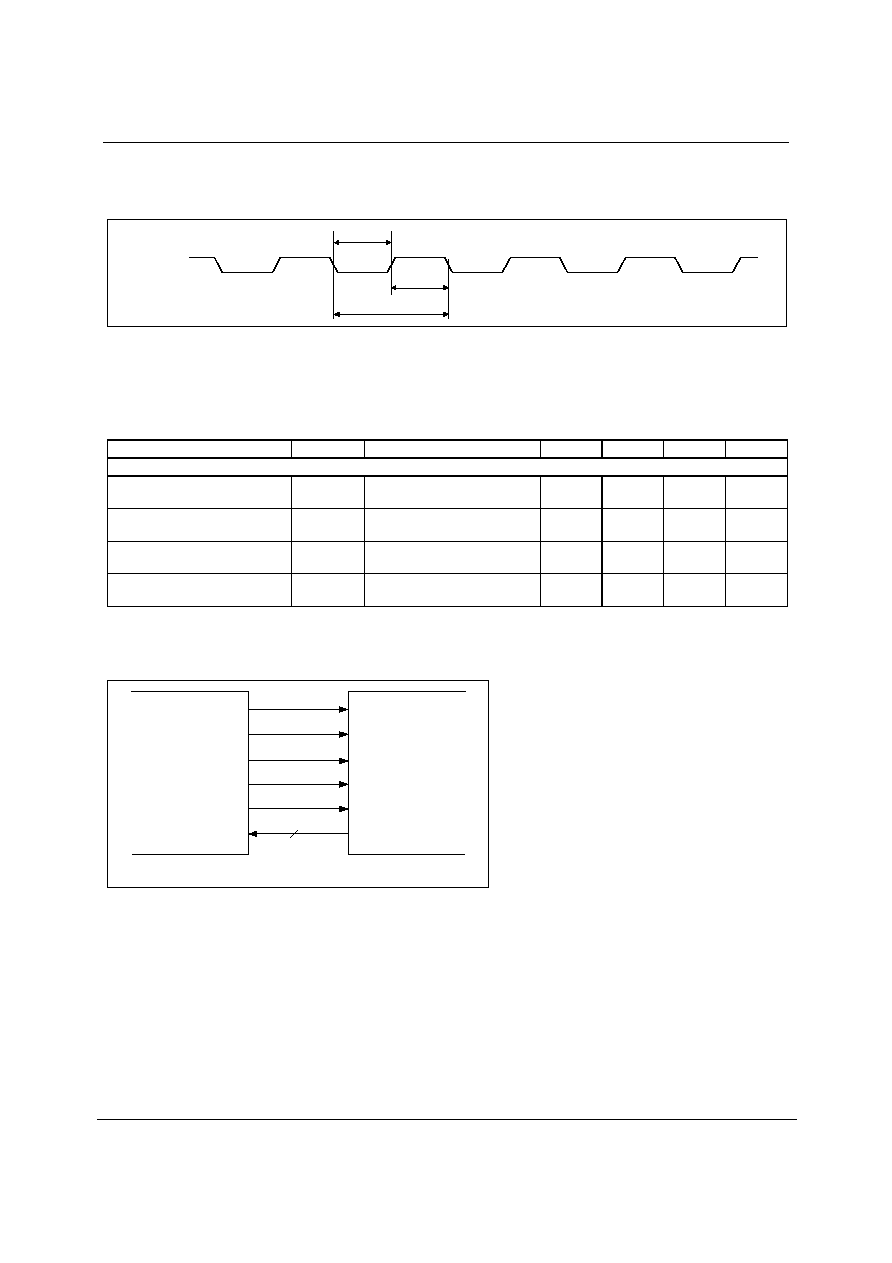
Production Data
WM8772EFT ≠ 32 PIN TQFP
w
PD Rev 4.1 October 2004
41
WM8722EFT - 32 PIN TQFP
MASTER CLOCK TIMING
ADCMCLK/
DACMCLK
t
MCLKL
t
MCLKH
t
MCLKY
Figure 33 ADC and DAC Master Clock Timing Requirements
Test Conditions
AVDD, VREFP = 5V, DVDD = 3.3V, AGND, VREFN = 0V, AGND, DGND = 0V, T
A
= +25
o
C, fs = 48kHz, DACMCLK and
ADCMCLK = 256fs unless otherwise stated.
PARAMETER SYMBOL
TEST
CONDITIONS
MIN
TYP
MAX
UNIT
System Clock Timing Information
ADCMCLK and DACMCLK
System clock pulse width high
t
MCLKH
11
ns
ADCMCLK and DACMCLK
System clock pulse width low
t
MCLKL
11
ns
ADCMCLK and DACMCLK
System clock cycle time
t
MCLKY
28
ns
ADCMCLK and DACMCLK Duty
cycle
40:60
60:40
Table 13 Master Clock Timing Requirements
DIGITAL AUDIO INTERFACE ≠ MASTER MODE
ADCLRC
DOUT
DACBCLK
DIN1/2/3
DACLRC
WM8772
CODEC
DSP/
ENCODER/
DECODER
3
ADCBCLK
Figure 34 Audio Interface - Master Mode

WM8772EFT ≠ 32 PIN TQFP
Production Data
w
PD Rev 4.1 October 2004
42
ADCBCLK/
DACBCLK
(Outputs)
DOUT
ADCLRC/
DACLRC
(Outputs)
t
DL
DIN1/2/3
t
DDA
t
DHT
t
DST
Figure 35 Digital Audio Data Timing ≠ Master Mode
Test Conditions
AVDD, VREFP = 5V, DVDD = 3.3V, AGND, VREFN, DGND = 0V, T
A
= +25
o
C, Master Mode, fs = 48kHz, DACMCLK and
ADCMCLK = 256fs unless otherwise stated.
PARAMETER SYMBOL
TEST
CONDITIONS
MIN
TYP
MAX
UNIT
Audio Data Input Timing Information
ADCLRC/DACLRC
propagation delay from
ADCBCLK/DACBCLK
falling edge
t
DL
0
10
ns
DOUT propagation delay
from ADCBCLK falling edge
t
DDA
0
10
ns
DIN1/2/3 setup time to
DACBCLK rising edge
t
DST
10
ns
DIN1/2/3 hold time from
DACBCLK rising edge
t
DHT
10
ns
Table 14 Digital Audio Data Timing ≠ Master Mode
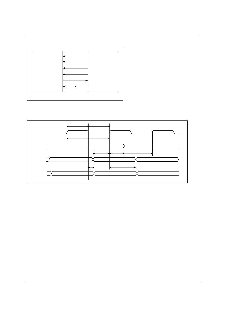
Production Data
WM8772EFT ≠ 32 PIN TQFP
w
PD Rev 4.1 October 2004
43
DIGITAL AUDIO INTERFACE ≠ SLAVE MODE
ADCLRC
DOUT
DACBCLK
DIN1/2/3
DACLRC
WM8772
CODEC
DSP
ENCODER/
DECODER
3
ADCBCLK
Figure 36 Audio Interface ≠ Slave Mode
DACBCLK/
ADCBCLK
DACLRC/
ADCLRC
t
BCH
t
BCL
t
BCY
DIN1/2/3
DOUT
t
LRSU
t
DS
t
LRH
t
DH
t
DD
Figure 37 Digital Audio Data Timing ≠ Slave Mode
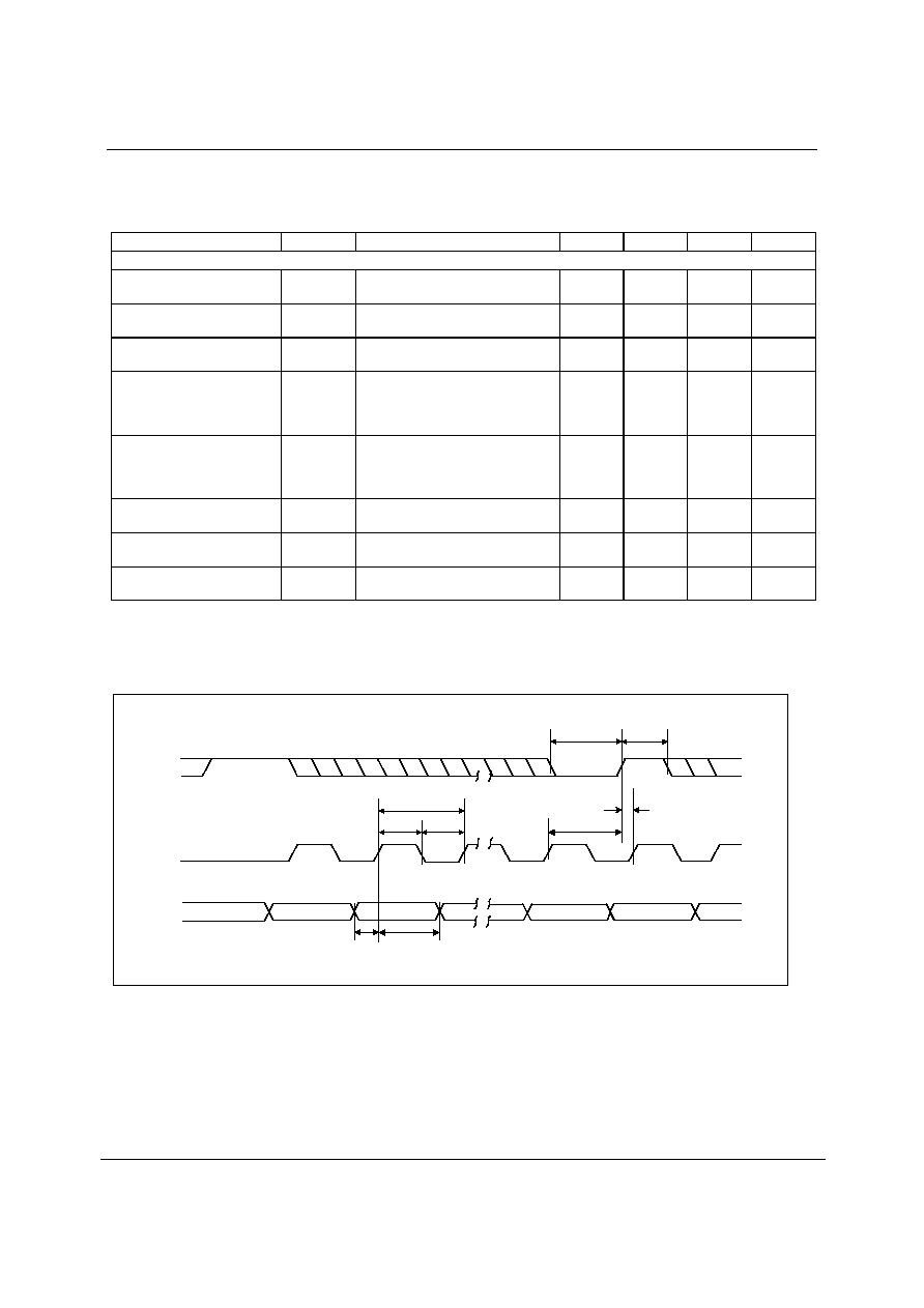
WM8772EFT ≠ 32 PIN TQFP
Production Data
w
PD Rev 4.1 October 2004
44
Test Conditions
AVDD = 5V, DVDD = 3.3V, AGND = 0V, DGND = 0V, T
A
= +25
o
C, Slave Mode, fs = 48kHz, DACMCLK and ADCMCLK = 256fs
unless otherwise stated.
PARAMETER SYMBOL
TEST
CONDITIONS
MIN
TYP
MAX
UNIT
Audio Data Input Timing Information
ADCBCLK/DACBCLK cycle
time
t
BCY
50
ns
ADCBCLK/DACBCLK pulse
width high
t
BCH
20
ns
ADCBCLK/DACBCLK pulse
width low
t
BCL
20
ns
ADCLRC/DACLRC set-up
time to
ADCBCLK/DACBCLK rising
edge
t
LRSU
10
ns
ADCLRC/DACLRC hold
time from
ADCBCLK/DACBCLK rising
edge
t
LRH
10
ns
DIN1/2/3 set-up time to
DACBCLK rising edge
t
DS
10
ns
DIN1/2/3 hold time from
DACBCLK rising edge
t
DH
10
ns
DOUT propagation delay
from ADCBCLK falling edge
t
DD
0
10
ns
Table 15 Digital Audio Data Timing ≠ Slave Mode
MPU INTERFACE TIMING
ML/I2S
MC/IWL
MD/DM
t
CSL
t
DHO
t
DSU
t
CSH
t
SCY
t
SCH
t
SCL
t
SCS
LSB
t
CSS
Figure 38 SPI Compatible Control Interface Input Timing

Production Data
WM8772EFT ≠ 32 PIN TQFP
w
PD Rev 4.1 October 2004
45
Test Conditions
AVDD = 5V, DVDD = 3.3V, AGND, DGND = 0V, T
A
= +25
o
C, fs = 48kHz, DACMCLK and ADCMCLK = 256fs unless otherwise
stated
PARAMETER SYMBOL
MIN
TYP
MAX
UNIT
MC/IWL rising edge to ML/I2S rising edge
t
SCS
60
ns
MC/IWL pulse cycle time
t
SCY
80
ns
MC/IWL pulse width low
t
SCL
30
ns
MC/IWL pulse width high
t
SCH
30
ns
MD/DM to MC/IWL set-up time
t
DSU
20
ns
MC/IWL to MD/DM hold time
t
DHO
20
ns
ML/I2S pulse width low
t
CSL
20
ns
ML/I2S pulse width high
t
CSH
20
ns
ML/I2S rising to MC/IWL rising
t
CSS
20
ns
Table 16 3-Wire SPI Compatible Control Interface Input Timing Information

WM8772EFT ≠ 32 PIN TQFP
Production Data
w
PD Rev 4.1 October 2004
46
DEVICE DESCRIPTION
INTRODUCTION
WM8772EFT is a complete 6-channel DAC, 2-channel ADC audio codec, including digital
interpolation and decimation filters, multi-bit sigma delta stereo ADC, and switched capacitor multi-
bit sigma delta DACs with digital volume controls on each channel and output smoothing filters.
The device is implemented as three separate stereo DACs and a stereo ADC in a single package
and controlled by a single interface.
Each stereo DAC has its own data input DIN1/2/3. DAC word clock DACLRC, DAC bit clock
DACBCLK and DAC master clock DACMCLK are shared between them. The stereo ADC has it's
own data output DOUT, word clock ADCLRC, bit clock ADCBCLK and ADC master clock ADCMCLK.
This allows the ADC and DAC to run independently.
The Audio Interface may be configured to operate in either master or slave mode. In Slave mode
ADCLRC and ADCBCLK, DACLRC and DACBCLK are all inputs. In Master mode ADCLRC and
ADCBCLK, DACLRC and DACBCLK are all outputs. The DAC's and ADC can be in any combination
of master or slave mode.
Each DAC has its own digital volume control that is adjustable in 0.5dB steps. The digital volume
controls may be operated independently. In addition, a zero cross detect circuit is provided for each
DAC for the digital volume controls. The digital volume control detects a transition through the zero
point before updating the volume. This minimises audible clicks and `zipper' noise as the gain values
change.
Control of internal functionality of the device is by 3-wire serial or pin programmable control interface.
The software control interface may be asynchronous to the audio data interface as control data will
be re-synchronised to the audio processing internally.
Operation using master clocks of 128fs, 192fs, 256fs, 384fs, 512fs or 768fs is provided for the DAC,
and 256fs, 384fs, 512fs, and 768fs is provided for the ADC. In Slave mode selection between clock
rates is automatically controlled. In master mode, the sample rate is set by control bits ADCRATE
and DACRATE. Audio sample rates (fs) from less than 8ks/s up to 192ks/s are allowed for the DAC
and from less than 32ks/s up to 96ks/s for the ADC, provided the appropriate master clock is input.
The audio data interface supports right, left and I
2
S interface formats along with a highly flexible DSP
serial port interface.
AUDIO DATA SAMPLING RATES
In a typical digital audio system there is only one central clock source producing a reference clock to
which all audio data processing is synchronised. This clock is often referred to as the audio system's
Master Clock. The external master system clock can be applied directly through the ADC and DAC
MCLK input pin(s) with no software configuration necessary. In a system where there are a number
of possible sources for the reference clock it is recommended that the clock source with the lowest
jitter be used to optimise the performance of the ADC and DAC.
The DAC master clock for WM8772EFT supports audio sampling rates from 128fs to 768fs, where fs
is the audio sampling frequency (DACLRC) typically 32kHz, 44.1kHz, 48kHz, 96kHz or 192kHz (for
DAC operation only). The ADC master clock for WM8772EFT supports audio sampling rates from
256fs to 768fs, where fs is the audio sampling frequency (ADCLRC) typically 32kHz, 44.1kHz,
48kHz, 96kHz or 192kHz. The master clock is used to operate the digital filters and the noise shaping
circuits.
In Slave mode the WM8772EFT has a master clock detection circuit that automatically determines
the relationship between the system clock frequency and the sampling rate (to within +/- 32 master
clocks). If there is a greater than 32 clocks error the interface defaults to 768fs mode. The master
clocks must be synchronised with ADCLRC and DACLRC respectively, although the WM8772EFT is
tolerant of phase variations or jitter on this clock. Table 6 shows the typical master clock frequency
inputs for the WM8772EFT.
Production Data
WM8772EFT ≠ 32 PIN TQFP
w
PD Rev 4.1 October 2004
47
The signal processing for the WM8772EFT typically operates at an oversampling rate of 128fs for
both ADC and DAC. The exception to this for the DAC is for operation with a 128/192fs system clock,
e.g. for 192kHz operation, when the oversampling rate is 64fs. For ADC operation at 96kHz it is
recommended that the user set the ADCOSR bit. This changes the ADC signal processing
oversample rate to 64fs.
System Clock Frequency (MHz)
SAMPLING
RATE
(DACLRC/
ADCLRC)
128fs 192fs 256fs 384fs 512fs 768fs
32kHz 4.096 6.144 8.192 12.288
16.384 24.576
44.1kHz 5.6448 8.467 11.2896
16.9340
22.5792 33.8688
48kHz 6.144 9.216 12.288
18.432
24.576 36.864
96kHz 12.288
18.432 24.576 36.864
Unavailable
Unavailable
192kHz 24.576 36.864
Unavailable
Unavailable
Unavailable
Unavailable
Table 17 System Clock Frequencies Versus Sampling Rate
(ADC does not support 128fs and 192fs)
HARDWARE CONTROL MODES
When the MODE pin is held high, the following hardware modes of operation are available.
Note: When in hardware mode the ADC and DAC will only run in slave mode.
MUTE AND AUTOMUTE OPERATION
In both hardware and software modes, MUTE controls the selection of MUTE directly, and can be
used to enable and disable the automute function. This pin becomes an output when left floating and
indicates infinite ZERO detect (IZD) has been detected.
DESCRIPTION
0 Normal
Operation
1
Mute DAC channels
Floating
Enable IZD, MUTE becomes an output to indicate when IZD occurs.
L=IZD detected, H=IZD not detected.
Table 18 Mute and Automute Control
Figure 39 shows the application and release of MUTE whilst a full amplitude sinusoid is being played
at 48kHz sampling rate. When MUTE (lower trace) is asserted, the output (upper trace) begins to
decay exponentially from the DC level of the last input sample. The output will decay towards V
MID
with a time constant of approximately 64 input samples. If MUTE is applied to all channels for 1024
or more input samples the outputs will be connected directly to V
MID
if IZD is set. When MUTE is de-
asserted, the output will restart immediately from the current input sample.
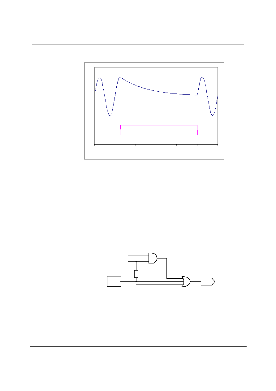
WM8772EFT ≠ 32 PIN TQFP
Production Data
w
PD Rev 4.1 October 2004
48
Figure 39 Application and Release of Soft Mute
The MUTE pin is an input to select mute or not mute. MUTE is active high; taking the pin high causes
the filters to soft mute, ramping down the audio signal over a few milliseconds. Taking MUTE low
again allows data into the filter.
The automute function detects a series of ZERO value audio samples of 1024 samples long being
applied to both channels. After such an event, a latch is set whose output (AUTOMUTED) is wire
OR'ed through a 10k resistor to the MUTE pin. Thus if the MUTE pin is not being driven, the
automute function will assert mute.
If MUTE is tied low, AUTOMUTED is overridden and will not mute unless the IZD register bit is set. If
MUTE is driven from a bi-directional source, then both MUTE and automute functions are available. If
MUTE is not driven, AUTOMUTED appears as a weak output (10k source impedance) and can be
used to drive external mute circuits. AUTOMUTED will be removed as soon as any channel receives
a non-ZERO input.
A diagram showing how the various Mute modes interact is shown below Figure 20.
IZD (Register Bit)
AUTOMUTED
(Internal Signal)
10k
MUTE (Register Bit)
SOFTMUTE
(Internal
Signal)
MUTE
PIN
Figure 40 Selection Logic for MUTE Modes
-2.5
-2
-1.5
-1
-0.5
0
0.5
1
1.5
0
0.001
0.002
0.003
0.004
0.005
0.006
Time(s)

Production Data
WM8772EFT ≠ 32 PIN TQFP
w
PD Rev 4.1 October 2004
49
INPUT FORMAT SELECTION
In hardware mode, ML/I2S and MC/IWL become input controls for selection of input data format type
and input data word length for both the ADC and DAC.
ML/I2S MC/IWL
INPUT
DATA
MODE
0 0
24-bit right justified
0 1
20-bit right justified
1 0
16-bit I
2
S
1 1
24-bit I
2
S
Table 19 Input Format Selection
Note:
In 24 bit I
2
S mode, any width of 24 bits or less is supported provided that the left/right clocks
(ADCLRC and DACLRC) are high for a minimum of 24 bit clocks (ADCBCLK and DACBCLK) and
low for a minimum of 24 bit clocks.
DE-EMPHASIS CONTROL
In hardware mode, the MD/DM pin becomes an input control for selection of de-emphasis filtering to
be applied.
MD/DM DE-EMPHASIS
0 Off
1 On
Table 20 De-emphasis Control
DIGITAL AUDIO INTERFACE
MASTER AND SLAVE MODES
The audio interface operates in either Slave or Master mode, selectable using the DACMS and
ADCMS control bits. In both Master and Slave modes DIN1/2/3 are always inputs to the
WM8772EFT and DOUT is always an output. The default is Slave mode for ADC and DAC.
In Slave mode, ADCLRC, DACLRC and ADCBCLK, DACBCLK are inputs to the WM8772EFT
(Figure 21). DIN1/2/3, ADCLRC and DACLRC are sampled by the WM8772EFT on the rising edge of
ADCBCLK and DACBCLK respectively. ADC data is output on DOUT and changes on the falling
edge of ADCBCLK.
By setting the control bit DACBCP the polarity of DACBCLK may be reversed so that DIN1/2/3 and
DACLRC are sampled on the falling edge of DACBCLK.
By setting the control bit ADCBCP the polarity of ADCBCLK may be reversed so that ADCLRC is
sampled on the falling edge of ADCBCLK and DOUT changes on the rising edge of ADCBCLK.
ADCLRC
DOUT
DACBCLK
DIN1/2/3
DACLRC
WM8772
CODEC
DSP
ENCODER/
DECODER
3
ADCBCLK
Figure 41 Slave Mode
In Master mode, ADCLRC, DACLRC, ADCBCLK and DACBCLK are outputs from the WM8772EFT
(Figure 22). ADCLRC, DACLRC, ADCBCLK and DACBCLK are generated by the WM8772EFT.

WM8772EFT ≠ 32 PIN TQFP
Production Data
w
PD Rev 4.1 October 2004
50
DIN1/2/3 are sampled by the WM8772EFT on the rising edge of DACBCLK so the controller must
output DAC data that changes on the falling edge of DACBCLK. ADC data is output on DOUT and
changes on the falling edge of ADCBCLK.
By setting control bit DACBCP the polarity of DACBCLK may be reversed so that DIN1/2/3 are
sampled on the falling edge of DACBCLK.
By setting control bit ADCBCP the polarity of ADCBCLK may be reversed so that DOUT changes on
the rising edge of ADCBCLK.
ADCLRC
DOUT
DACBCLK
DIN1/2/3
DACLRC
WM8772
CODEC
DSP/
ENCODER/
DECODER
3
ADCBCLK
Figure 42 Master Mode
AUDIO INTERFACE FORMATS
Audio data is applied to the internal DAC filters, or output from the ADC filters, via the Digital Audio
Interface. 5 popular interface formats are supported:
∑
Left Justified mode
∑
Right Justified mode
∑
I
2
S mode
∑
DSP
Early
mode
∑
DSP Late mode
All 5 formats send the MSB first and support word lengths of 16, 20, 24 and 32 bits, with the
exception of 32 bit right justified mode, which is not supported.
In left justified, right justified and I
2
S modes, the digital audio interface receives DAC data on the
DIN1/2/3 inputs and outputs ADC data on DOUT. Audio Data for each stereo channel is time
multiplexed with ADCLRC or DACLRC indicating whether the left or right channel is present.
ADCLRC or DACLRC is also used as a timing reference to indicate the beginning or end of the data
words.
In left justified, right justified and I
2
S modes, the minimum number of DACBCLK/ADCBCLK's per
DACLRC/ADCLRC period is 2 times the selected word length. ADCLRC/DACLRC must be high for a
minimum of word length DACBCLK/ADCBCLK's and low for a minimum of word length
DACBCLK/ADCBCLK's. Any mark to space ratio on ADCLRC/DACLRC is acceptable provided the
above requirements are met.
In DSP early or DSP late mode, all 6 DAC channels are time multiplexed onto DIN1. DACLRC is
used as a frame sync signal to identify the MSB of the first word. The minimum number of
DACBCLK's per DACLRC period is 6 times the selected word length. Any mark to space ratio is
acceptable on DACLRC provided the rising edge is correctly positioned. The ADC data may also be
output in DSP early or late modes, with ADCLRC used as a frame sync to identify the MSB of the
first word. The minimum number of ADCBCLK's per ADCLRC period is 2 times the selected word
length
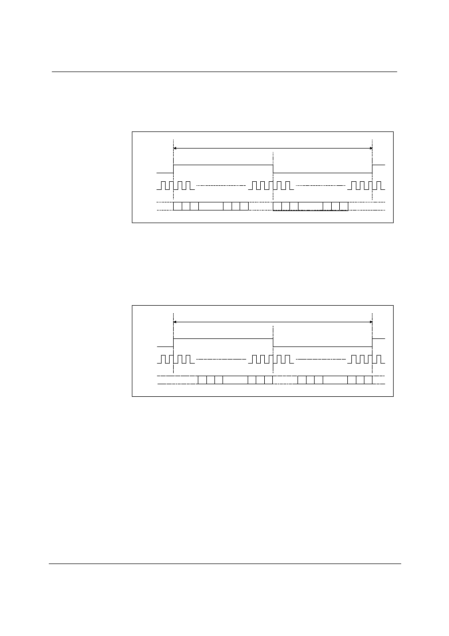
Production Data
WM8772EFT ≠ 32 PIN TQFP
w
PD Rev 4.1 October 2004
51
LEFT JUSTIFIED MODE
In left justified mode, the MSB of DIN1/2/3 is sampled by the WM8772EFT on the first rising edge of
DACBCLK following a DACLRC transition. The MSB of the ADC data is output on DOUT and
changes on the same falling edge of ADCBCLK as ADCLRC and may be sampled on the rising edge
of ADCBCLK. ADCLRC and DACLRC are high during the left samples and low during the right
samples (Figure 43).
LEFT CHANNEL
RIGHT CHANNEL
DACLRC/
ADCLRC
DACBCLK/
ADCBCLK
DIN1/2/3/
DOUT
1/fs
n
3
2
1
n-2 n-1
LSB
MSB
n
3
2
1
n-2 n-1
LSB
MSB
Figure 43 Left Justified Mode Timing Diagram
RIGHT JUSTIFIED MODE
In right justified mode, the LSB of DIN1/2/3 is sampled by the WM8772EFT on the rising edge of
DACBCLK preceding a DACLRC transition. The LSB of the ADC data is output on DOUT and
changes on the falling edge of ADCBCLK preceding a ADCLRC transition and may be sampled on
the rising edge of ADCBCLK. ADCLRC and DACLRC are high during the left samples and low during
the right samples (Figure 44).
LEFT CHANNEL
RIGHT CHANNEL
DACLRC/
ADCLRC
DACBCLK/
ADCBCLK
DIN1/2/3/
DOUT
1/fs
n
3
2
1
n-2 n-1
LSB
MSB
n
3
2
1
n-2 n-1
LSB
MSB
Figure 44 Right Justified Mode Timing Diagram
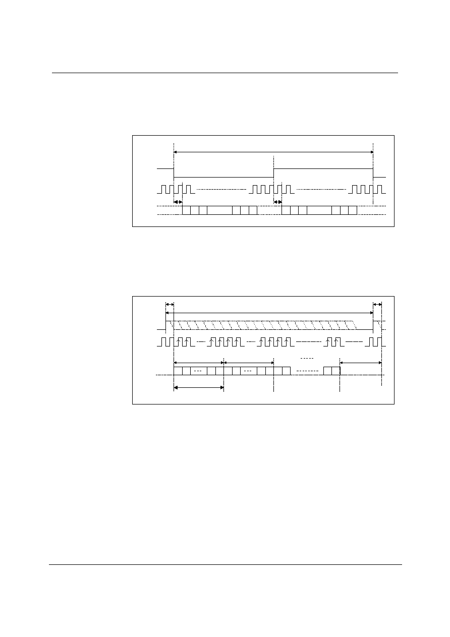
WM8772EFT ≠ 32 PIN TQFP
Production Data
w
PD Rev 4.1 October 2004
52
I
2
S MODE
In I
2
S mode, the MSB of DIN1/2/3 is sampled by the WM8772EFT on the second rising edge of
BCLK following a DACLRC transition. The MSB of the ADC data is output on DOUT and changes on
the first falling edge of BCLK following an ADCLRC transition and may be sampled on the rising edge
of BCLK. ADCLRC and DACLRC are low during the left samples and high during the right samples.
LEFT CHANNEL
RIGHT CHANNEL
DACLRC/
ADCLRC
DACBCLK/
ADCBCLK
DIN1/2/3/
DOUT
1/fs
n
3
2
1
n-2 n-1
LSB
MSB
n
3
2
1
n-2 n-1
LSB
MSB
1 BCLK
1 BCLK
Figure 45 I
2
S Mode Timing Diagram
DSP EARLY MODE
In DSP early mode, the MSB of DAC channel 1 left data is sampled by the WM8772EFT on the
second rising edge on DACBCLK following a DACLRC rising edge. DAC channel 1 right and DAC
channels 2 and 3 data follow DAC channel 1 left data (Figure 46).
DACLRC
DACBCLK
DIN1
Input Word Length (IWL)
1/fs
CHANNEL 1
LEFT
n
2
1
n-1
LSB
MSB
n
2
1
n-1
CHANNEL 1
RIGHT
2
1
CHANNEL 2
LEFT
n
n-1
CHANNEL 3
RIGHT
NO VALID DATA
1 BCLK
1 BCLK
Figure 46 DSP Early Mode Timing Diagram ≠ DAC Data Input
The MSB of the left channel ADC data is output on DOUT and changes on the first falling edge of
ADCBCLK following a low to high ADCLRC transition and may be sampled on the rising edge of
ADCBCLK. The right channel ADC data is contiguous with the left channel data (Figure 47)
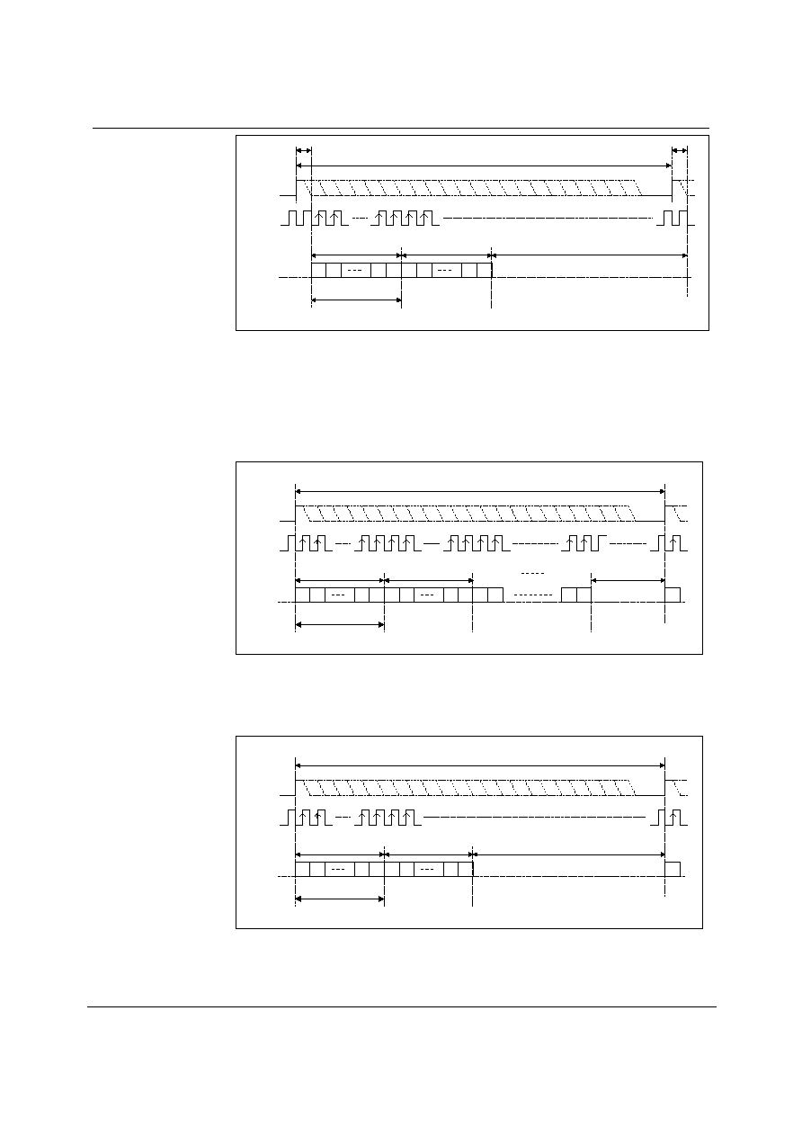
Production Data
WM8772EFT ≠ 32 PIN TQFP
w
PD Rev 4.1 October 2004
53
ADCLRC
ADCBCLK
DOUT
Input Word Length (IWL)
1/fs
LEFT CHANNEL
n
2
1
n-1
LSB
MSB
n
2
1
n-1
RIGHT CHANNEL
NO VALID DATA
1 BCLK
1 BCLK
Figure 47 DSP Early Mode Timing Diagram ≠ ADC Data Output
DSP LATE MODE
In DSP late mode, the MSB of DAC channel 1 left data is sampled by the WM8772EFT on the first
DACBCLK rising edge following a DACLRC rising edge. DAC channel 1 right and DAC channels 2
and 3 data follow DAC channel 1 left data (Figure 48).
DACLRC
DACBCLK
DIN1
Input Word Length (IWL)
1/fs
CHANNEL 1
LEFT
n
2
1
n-1
LSB
MSB
n
2
1
n-1
CHANNEL 1
RIGHT
2
1
CHANNEL 2
LEFT
n
n-1
CHANNEL 3
RIGHT
NO VALID DATA
1
Figure 48 DSP Late Mode Timing Diagram ≠ DAC Data Input
The MSB of the left channel ADC data is output on DOUT and changes on the same falling edge of
ADCBCLK as the low to high ADCLRC transition and may be sampled on the rising edge of
ADCBCLK. The right channel ADC data is contiguous with the left channel data (Figure 49).
ADCLRC
BCK
DOUT
Input Word Length (IWL)
1/fs
LEFT CHANNEL
n
2
1
n-1
LSB
MSB
n
2
1
n-1
RIGHT CHANNEL
NO VALID DATA
1
Figure 49 DSP Late Mode Timing Diagram ≠ ADC Data Output
In both early and late DSP modes, DACL1 is always sent first, followed immediately by DACR1 and
the data words for the other 6 channels. No BCLK edges are allowed between the data words. The
word order is DAC1 left, DAC1 right, DAC2 left, DAC2 right, DAC3 left, DAC3 right.
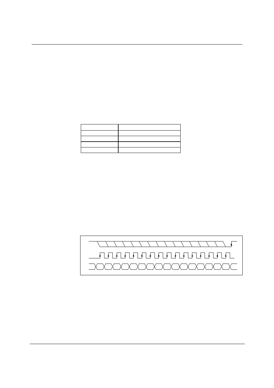
WM8772EFT ≠ 32 PIN TQFP
Production Data
w
PD Rev 4.1 October 2004
54
POWERDOWN MODES
The WM8772EFT has powerdown control bits allowing specific parts of the WM8772EFT to be
powered off when not being used. Control bit ADCPD powers off the ADC. The three stereo DACs
each have a separate powerdown control bit, DACPD[2:0] allowing individual stereo DACs to be
powered off when not in use. Setting ADCPD and DACPD[2:0] will powerdown everything except the
references VMID and REFADC. These may be powered down by setting PDWN. Setting PDWN will
override all other powerdown control bits. It is recommended that the ADC and DACs are powered
down before setting PDWN.
ZERO DETECT
The WM8772EFT has a zero detect circuit for each DAC channel that detects when 1024
consecutive zero samples have been input. The MUTE pin output may be programmed to output the
zero detect signal (see Table 10) which may then be used to control external muting circuits. A `1' on
MUTE indicates a zero detect. The zero detect may also be used to automatically enable DAC mute
by setting IZD.
DZFM[1:0] MUTE
00 All
channels
zero
01 Channel
1
zero
10 Channel
2
zero
11 Channel
3
zero
Table 21 Zero Flag Output Select
SOFTWARE CONTROL INTERFACE OPERATION
The WM8772EFT is controlled using a 3-wire serial interface in software mode or pin programmable
in hardware mode.
The control mode is selected by the state of the MODE pin.
The control interfaces are 5V tolerant; meaning that the control interface input signals ML/I2S,
MC/IWL and MD/DM may have an input high level of 5V while DVDD is 3V. Input thresholds are
determined by DVDD. MUTE and MODE are also 5V tolerant.
3-WIRE (SPI COMPATIBLE) SERIAL CONTROL MODE
MD/DM is used for the program data, MC/IWL is used to clock in the program data and ML/I2S is
used to latch the program data. MD/DM is sampled on the rising edge of MC/IWL. The 3-wire
interface protocol is shown in Figure 30.
B15 B14 B13 B12 B11 B10 B9 B8 B7 B6 B5 B4 B3 B2 B1 B0
ML/I2S
MC/IWL
MD/DM
Figure 50 3-Wire SPI Compatible Interface
4.
B[15:9] are Control Address Bits
5.
B[8:0] are Control Data Bits
6.
ML/I2S is edge-sensitive ≠ the data is latched on the rising edge of ML/I2S.
Production Data
WM8772EFT ≠ 32 PIN TQFP
w
PD Rev 4.1 October 2004
55
REGISTER MAP ≠ 32 PIN TQFP
The complete register map is shown below. The detailed description can be found in the relevant text of the device description. The
WM8772EFT can be configured using the Control Interface. All unused bits should be set to `0'.
REGISTER
B15
B14
B13
B12
B11
B10
B9
B8
B7
B6
B5
B4
B3
B2
B1
B0
DEFAULT
R0(00h)
0
0
0
0
0
0
0
UPDATE LDA1[7:0] 011111111
R1(01h)
0
0
0
0
0
0
1
UPDATE RDA1[7:0] 011111111
R2(02h)
0
0
0
0
0
1
0
PL[8:5]
IZD ATC
PDWN
All DAC
DEEMP
MUTE
All DAC
100100000
R3(03h)
0
0
0
0
0
1
1
PHASE[8:6]
DACIWL[5:4] DACBCP
DACLRP DACFMT[1:0]
000000000
R4(04h)
0
0
0
0
1
0
0
UPDATE LDA2[7:0] 011111111
R5(05h)
0
0
0
0
1
0
1
UPDATE RDA2[7:0] 011111111
R6(06h)
0
0
0
0
1
1
0
UPDATE LDA3[7:0] 011111111
R7(07h)
0
0
0
0
1
1
1
UPDATE RDA3[7:0] 011111111
R8(08h)
0
0
0
1
0
0
0
UPDATE MASTDA[7:0] 011111111
R9(09h)
0
0
0
1
0
0
1
DEEMP[8:6]
DMUTE[5:3] DZFM[2:1]
ZCD 000000000
R10(0Ah)
0
0
0
1
0
1
0
DACRATE[8:6] DACMS
PWRDN
ALL
DACPD[3:1]
ADCPD 010000000
R11(0Bh)
0
0
0
1
0
1
1
ADC
OSR
ADCRATE[7:5] ADCMS
ADCIWL[3:2]
ADCFMT[1:0]
001000000
R12(0Ch)
0
0
0
1
1
0
0
0 SYNC
MPD
ADCBCP
ADCLRP
ADCHP
AMUTE
ALL
AMUTEL AMUTER 000000000
R31(1Fh)
0
0
1
1
1
1
1
RESET
000000000
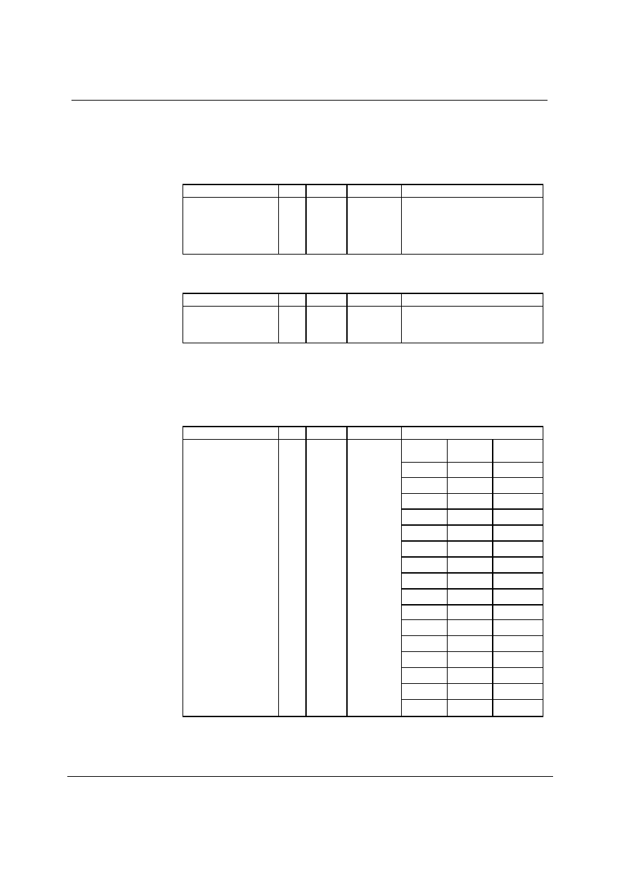
WM8772EFT ≠ 32 PIN TQFP
Production Data
w
PD Rev 4.1 October 2004
56
CONTROL INTERFACE REGISTERS
ATTENUATOR CONTROL MODE
Setting the ATC register bit causes the left channel attenuation settings to be applied to both left and
right channel DACs from the next audio input sample. No update to the attenuation registers is
required for ATC to take effect.
REGISTER ADDRESS
BIT
LABEL
DEFAULT
DESCRIPTION
0000010
DAC Channel Control
3 ATC
0
Attenuator Control Mode:
0: Right channels use right
attenuations
1: Right channels use left
attenuations
INFINITE ZERO DETECT ENABLE
Setting the IZD register bit will enable the internal infinite zero detect function:
REGISTER ADDRESS
BIT
LABEL
DEFAULT
DESCRIPTION
0000010
DAC Channel Control
4 IZD
0 Infinite zero mute enable
0: Disable infinite zero mute
1: Enable infinite zero mute
With IZD enabled, applying 1024 consecutive zero input samples to each input will cause the
relevant DAC to be muted to V
MID
. Mute will be removed as soon as that channel receives a non-zero
input.
DAC OUTPUT CONTROL
The DAC output control word determines how the left and right inputs to the audio Interface are
applied to the left and right DACs:
REGISTER ADDRESS
BIT
LABEL
DEFAULT
DESCRIPTION
PL[3:0] Left
Output
Right
Output
0000 Mute Mute
0001 Left Mute
0010 Right Mute
0011 (L+R)/2
Mute
0100 Mute Left
0101 Left Left
0110 Right Left
0111 (L+R)/2
Left
1000 Mute Right
1001 Left Right
1010 Right Right
1011 (L+R)/2
Right
1100 Mute (L+R)/2
1101 Left (L+R)/2
1110 Right (L+R)/2
0000010
DAC Control
8:5 PL[3:0]
1001
1111 (L+R)/2
(L+R)/2
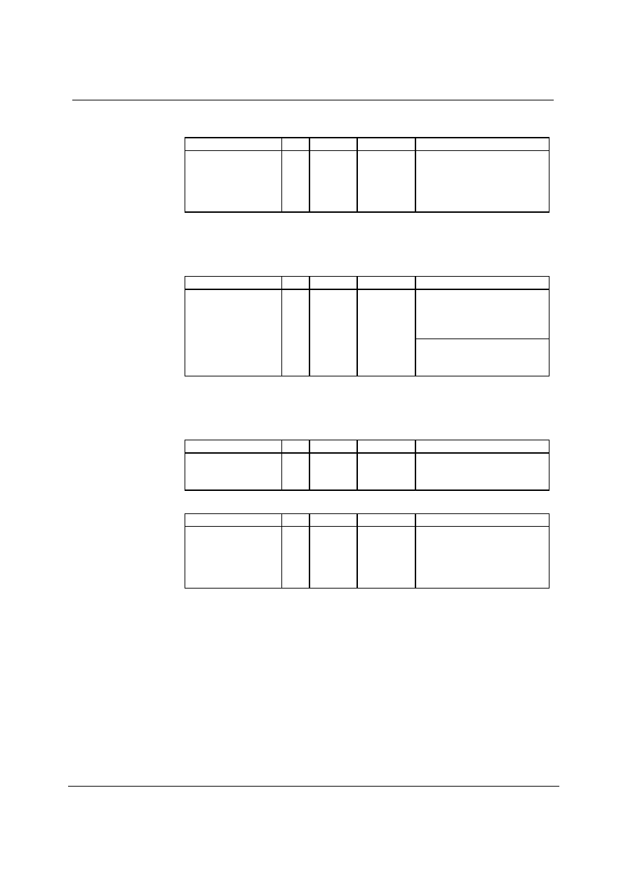
Production Data
WM8772EFT ≠ 32 PIN TQFP
w
PD Rev 4.1 October 2004
57
DAC DIGITAL AUDIO INTERFACE CONTROL REGISTER
Interface format is selected via the DACFMT[1:0] register bits:
REGISTER ADDRESS
BIT
LABEL
DEFAULT
DESCRIPTION
0000011
Interface Control
1:0 DACFMT
[1:0]
00
Interface Format Select:
00 : Right justified mode
01: Left justified mode
10:
I
2
S mode
11: DSP (early or late) mode
In left justified, right justified or I
2
S modes, the DACLRP register bit controls the polarity of DACLRC.
If this bit is set high, the expected polarity of DACLRC will be the opposite of that shown Figure 23,
Figure 24 and Figure 25. Note that if this feature is used as a means of swapping the left and right
channels, a 1 sample phase difference will be introduced. In DSP modes, the DACLRP register bit is
used to select between early and late modes.
REGISTER ADDRESS
BIT
LABEL
DEFAULT
DESCRIPTION
In Left/Right/I
2
S Modes:
DACLRC Polarity (normal)
0 : Normal DACLRC polarity
1: Inverted DACLRC polarity
0000011
Interface Control
2 DACLRP
0
In DSP Mode:
0 : Early DSP mode
1: Late DSP mode
By default, DACLRC and DIN1/2/3 are sampled on the rising edge of DACBCLK and should ideally
change on the falling edge. Data sources that change DACLRC and DIN1/2/3 on the rising edge of
DACBCLK can be supported by setting the BCP register bit. Setting DACBCP to 1 inverts the
polarity of DACBCLK to the inverse of that shown in Figure 23, Figure 24, Figure 25, Figure 26,
Figure 27, Figure 28 and Figure 29.
REGISTER ADDRESS
BIT
LABEL
DEFAULT
DESCRIPTION
0000011
Interface Control
3 DACBCP
0
DACBCLK Polarity (DSP Modes)
0 : Normal BCLK polarity
1: Inverted BCLK polarity
The DACIWL[1:0] bits are used to control the input word length.
REGISTER ADDRESS
BIT
LABEL
DEFAULT
DESCRIPTION
0000011
Interface Control
5:4 DACIWL
[1:0]
00
Input Word Length:
00 : 16 bit data
01: 20 bit data
10: 24 bit data
11: 32 bit data
Note: If 32-bit mode is selected in right justified mode, the WM8772EFT defaults to 24 bits.
In all modes, the data is signed 2's complement. The digital filters always input 24-bit data. If the
DAC is programmed to receive 16 or 20 bit data, the WM8772EFT pads the unused LSBs with zeros.
If the DAC is programmed into 32 bit mode, the 8 LSBs are ignored.
Note: In 24 bit I
2
S mode, any width of 24 bits or less is supported provided that DACLRC is high for a
minimum of 24 BCLKs and low for a minimum of 24 BCLKs.
A number of options are available to control how data from the Digital Audio Interface is applied to
the DAC channels.
WM8772EFT ≠ 32 PIN TQFP
Production Data
w
PD Rev 4.1 October 2004
58
DAC OUTPUT PHASE
The DAC Phase control word determines whether the output of each DAC is non-inverted or inverted
REGISTER ADDRESS
BIT
LABEL
DEFAULT
DESCRIPTION
Bit DAC
Phase
0 DAC1L/R
1
=
invert
1 DAC2L/R
1
=
invert
0000011
DAC Phase
8:6 PHASE
[2:0]
000
2 DAC3L/R
1
=
invert
DIGITAL ZERO CROSS-DETECT
The Digital volume control also incorporates a zero cross detect circuit which detects a transition
through the zero point before updating the digital volume control with the new volume. This is
enabled by control bit DZCEN.
REGISTER ADDRESS
BIT
LABEL
DEFAULT
DESCRIPTION
0001001
DAC Control
0 ZCD
0 DAC Digital Volume Zero Cross
Disable:
0: Zero cross detect enabled
1: Zero cross detect disabled
MUTE FLAG OUTPUT
The DZFM control bits allow the selection of the six DAC channel zero flag bits for output on the
MUTEB pin. A `1' on MUTE indicates 1024 consecutive zero input samples to the DAC channels
selected.
REGISTER ADDRESS
BIT
LABEL
DEFAULT
DESCRIPTION
0001001
Zero Flag
2:1 DZFM[1:0]
00
Selects the output MUTE pin (A `1'
indicates 1024 consecutive zero
input samples on the DAC
channels selected.
00: All channels zero
01: Channel 1 zero
10: Channel 2 zero
11: Channel 3 zero
DAC MUTE MODES
The WM8772EFT has individual mutes for each of the three DAC channels. Setting MUTE for a
channel will apply a `soft' mute to the input of the digital filters of the channel muted.
REGISTER ADDRESS
BIT
LABEL
DEFAULT
DESCRIPTION
0001001
DAC Mute
5:3 DMUTE
[2:0]
000
DAC Soft Mute Select
DMUTE [2:0]
DAC CHANNEL 1
DAC CHANNEL 2
DAC CHANNEL 3
000
Not MUTE
Not MUTE
Not MUTE
001 MUTE
Not
MUTE
Not
MUTE
010 Not
MUTE
MUTE
Not
MUTE
011 MUTE
MUTE
Not
MUTE
100
Not MUTE
Not MUTE
MUTE
101 MUTE
Not
MUTE
MUTE
110 Not
MUTE
MUTE MUTE

Production Data
WM8772EFT ≠ 32 PIN TQFP
w
PD Rev 4.1 October 2004
59
Setting the MUTEALL register bit will apply a 'soft' mute to the input of all the DAC digital filters:
REGISTER ADDRESS
BIT
LABEL
DEFAULT
DESCRIPTION
0000010
DAC Mute
0 MUTEALL
0
Soft Mute Select:
0 : Normal operation
1: Soft mute all channels
Refer to Figure 39 for the plot of application and release of soft mute.
Note that all other means of muting the DAC channels: setting the PL[3:0] bits to 0, setting the
PDWN bit or setting attenuation to 0 will cause much more abrupt muting of the output.
ADC MUTE MODES
Each ADC channel also has a mute control bit, which mutes the inputs to the ADC.
REGISTER ADDRESS
BIT
LABEL
DEFAULT
DESCRIPTION
0 AMUTER
0
ADC Mute Select:
0 : Normal operation
1: mute ADC right
1 AMUTEL
0 ADC Mute Select:
0 : Normal operation
1: mute ADC left
0001100
ADC Mute
2 AMUTEALL
0
ADC Mute Select:
0 : Normal operation
1: mute both ADC channels
DE-EMPHASIS MODE
Each stereo DAC channel has an individual de-emphasis control bit:
REGISTER ADDRESS
BIT
LABEL
DEFAULT
DESCRIPTION
0001001
DAC De-emphahsis
Control
[8:6]
DEEMPH
[1:0]
000
De-emphasis Channel Selection
Select:
DEEMPH
[1:0]
DAC CHANNEL 1
DAC CHANNEL 2
DAC CHANNEL 3
000
Not DE-EMPHASIS
Not DE-EMPHASIS
Not DE-EMPHASIS
001
DE-EMPHASIS
Not DE-EMPHASIS
Not DE-EMPHASIS
010 Not
DE-EMPHASIS
DE-EMPHASIS
Not
DE-EMPHASIS
011 DE-EMPHASIS
DE-EMPHASIS
Not
DE-EMPHASIS
100 Not
DE-EMPHASIS
Not
DE-EMPHASIS
DE-EMPHASIS
101 DE-EMPHASIS
Not
DE-EMPHASIS
DE-EMPHASIS
110 Not
DE-EMPHASIS
DE-EMPHASIS
DE-EMPHASIS
Refer to Figure 7, Figure 8, Figure 9, Figure 10, Figure 11 and Figure 12 for details of the De-
Emphasis performance at different sample rates.
REGISTER ADDRESS
BIT
LABEL
DEFAULT
DESCRIPTION
0000010
DAC DEMP
1 DEEMP
ALL
0
DEMMP Select:
0 : Normal operation
1: De-emphasis all channels
WM8772EFT ≠ 32 PIN TQFP
Production Data
w
PD Rev 4.1 October 2004
60
POWERDOWN MODE AND ADC/DAC DISABLE
Setting the PDWN register bit immediately powers down the DAC's on the WM8772EFT, overriding
the DACD powerdown bits control bits. All trace of the previous input samples are removed, but all
control register settings are preserved. When PDWN is cleared the digital filters will be reinitialised
REGISTER ADDRESS
BIT
LABEL
DEFAULT
DESCRIPTION
0000010
Powerdown Control
2 PDWN
0
Power Down all DAC's Select:
0: All DAC's enabled
1: All DAC's disabled
The ADC and DACs may also be powered down individually by setting the ADCPD and DACPD
disable bits. Setting ADCD will disable the ADC and select a low power mode. The ADC digital filters
will be reset and will reinitialise when ADCPD is unset. Each Stereo DAC channel has a separate
disable DACPD[2:0]. Setting DACPD for a channel will disable the DACs and select a low power
mode. Resetting DACD will reinitialise the digital filters.
REGISTER ADDRESS
BIT
LABEL
DEFAULT
DESCRIPTION
0 ADCPD
0 ADC Disable:
0:
Active
1:
Disable
0001010
Powerdown Control
3:1 DACPD
[2:0]
000
DAC Disable
DACPD [2:0]
DAC CHANNEL 1
DAC CHANNEL 2
DAC CHANNEL 3
000 Active Active Active
001 DISABLE Active Active
010 Active
DISABLE
Active
011 DISABLE DISABLE Active
100 Active
Active
DISABLE
101 DISABLE Active DISABLE
110 Active
DISABLE
DISABLE
111 DISABLE DISABLE DISABLE
MASTER POWERDOWN
This control bit powers down the references for the whole chop. Therefore for complete powerdown,
both the ADC and DACs should be powered down first before setting this bit.
REGISTER ADDRESS
BIT
LABEL
DEFAULT
DESCRIPTION
0001010
Interface Control
4 PWRDNALL
0
Master Power Down Bit:
0: Not powered down
1:
Powered
down
DAC MASTER MODE SELECT
Control bit DACMS selects between audio interface Master and Slave Modes. In Master mode
DACLRC and DACBCLK are outputs and are generated by the WM8772EFT. In Slave mode
DACCLRC, DACLRC and DACBCLK are inputs to WM8772EFT.
REGISTER ADDRESS
BIT
LABEL
DEFAULT
DESCRIPTION
0001010
Interface Control
5 DACMS
0 DAC Audio Interface
Master/Slave Mode Select:
0: Slave Mode
1: Master Mode
Production Data
WM8772EFT ≠ 32 PIN TQFP
w
PD Rev 4.1 October 2004
61
MASTER MODE DACLRC FREQUENCY SELECT
In Master mode the WM8772EFT generates DACLRC and DACBCLK. These clocks are derived
from the master clock and the ratio of DACMCLK to DACLRC is set by DACRATE.
REGISTER ADDRESS
BIT
LABEL
DEFAULT
DESCRIPTION
0001010
Interface Control
8:6 DACRATE
[2:0]
010
Master Mode
DACMCLK:DACLRC Ratio
Select:
000:
128fs
001:
192fs
010:
256fs
011:
384fs
100:
512fs
101:
768fs
ADC DIGITAL AUDIO INTERFACE CONTROL REGISTER
Interface format is selected via the ADCFMT[1:0] register bits:
REGISTER ADDRESS
BIT
LABEL
DEFAULT
DESCRIPTION
0001011
Interface Control
1:0 ADCFMT[1:0]
00
Interface Format Select
00: Right justified mode
01: Left justified mode
10:
I
2
S mode
11: DSP (early or late) mode
The ADCIWL[1:0] bits are used to control the input word length.
REGISTER ADDRESS
BIT
LABEL
DEFAULT
DESCRIPTION
0001011
Interface Control
3:2
ADCIWL[1:0]
00
Input Word Length
00: 16 bit data
01: 20 bit data
10: 24 bit data
11: 32 bit data
Note: 32-bit right justified mode is not supported.
In all modes, the data is signed 2's complement.
ADC MASTER MODE SELECT
Control bit ADCMS selects between audio interface Master and Slave Modes. In Master mode
ADCLRC and ADCBCLK are outputs and are generated by the WM8772EFT. In Slave mode
ADCLRC and ADCBCLK are inputs to WM8772EFT.
REGISTER ADDRESS
BIT
LABEL
DEFAULT
DESCRIPTION
0001011
Interface Control
4 ADCMS
0 ADC Audio Interface
Master/Slave Mode Select:
0: Slave mode
1: Master mode

WM8772EFT ≠ 32 PIN TQFP
Production Data
w
PD Rev 4.1 October 2004
62
MASTER MODE ADCLRC FREQUENCY SELECT
In Master mode the WM8772EFT generates ADCLRC and ADCBCLK. These clocks are derived
from the master clock and the ratio of ADCMCLK to ADCLRC is set by ADCRATE.
REGISTER ADDRESS
BIT
LABEL
DEFAULT
DESCRIPTION
0001011
ADCLRC and ADCBCLK
Frequency Select
7:5 ADCRATE
[2:0]
010
Master Mode
ADCMCLK:ADCLRC Ratio
Select:
010:
256fs
011:
384fs
100: 512fs
101:
768fs
ADC OVERSAMPLING RATE SELECT
For ADC operation at 96kHz it is recommended that the user set the ADCOSR bit. This changes the
ADC signal processing oversample rate to 64fs. The 64fs oversampling rate is only available in
modes were a 96KHz rate is supported, i.e. 256fs or 384fs. In all other modes the ADC will stay in a
128fs oversampling rate irrespective of what this bit is set to.
REGISTER ADDRESS
BIT
LABEL
DEFAULT
DESCRIPTION
0001011
ADC Oversampling Rate
8 ADCOSR
0
ADC Oversampling Rate Select
0:
128x
oversampling
1:
64x
oversampling
ADC HIGHPASS FILTER DISABLE
The ADC digital filters contain a digital highpass filter. This defaults to enabled and can be disabled
using software control bit ADCHPD.
REGISTER ADDRESS
BIT
LABEL
DEFAULT
DESCRIPTION
0001100
ADC Control
3
ADCHPD
0
ADC Highpass Filter Disable:
0: Highpass filter enabled
1: Highpass filter disabled
In left justified, right justified or I
2
S modes, the ADCLRP register bit controls the polarity of ADCLRC.
If this bit is set high, the expected polarity of ADCLRC will be the opposite of that shown Figure 23,
Figure 24 and Figure 25. Note that if this feature is used as a means of swapping the left and right
channels, a 1 sample phase difference will be introduced. In DSP modes, the ADCLRP register bit is
used to select between early and late modes.
REGISTER ADDRESS
BIT
LABEL
DEFAULT
DESCRIPTION
In Left/Right/I
2
S Modes:
ADCLRC Polarity (normal)
0: normal DACLRC polarity
1: inverted DACLRC polarity
0001100
Interface Control
4 ADCLRP
0
In DSP Mode:
0: Early DSP mode
1: Late DSP mode
By default, DACLRC and DOUT are sampled on the rising edge of ADCBCLK and should ideally
change on the falling edge. Data sources that change ADCLRC and DOUT on the rising edge of
ADCBCLK can be supported by setting the ADCBCP register bit. Setting ADCBCP to 1 inverts the
polarity of ADCBCLK to the inverse of that shown in Figure 23, Figure 24, Figure 25, Figure 26,
Figure 27, Figure 28 and Figure 29.
Production Data
WM8772EFT ≠ 32 PIN TQFP
w
PD Rev 4.1 October 2004
63
REGISTER ADDRESS
BIT
LABEL
DEFAULT
DESCRIPTION
0001100
Interface Control
5 ADCBCP
0
ADCBCLK Polarity (DSP Modes):
0: normal BCLK polarity
1: inverted BCLK polarity
MUTE PIN DECODE
The MUTE pin can either be used an output or an input. When used as an input the MUTE pins
action can controlled by setting the DZFM bit to select the corresponding DAC for applying the MUTE
to. As an output its meaning is selected by the DZFM control bits. By default selecting the MUTE to
represent if DAC1 has received more than 1024 midrail samples will cause the MUTE to be asserted
a softmute on DAC1. Disabling the decode block will cause any logical high on the MUTE pin to
apply a softmute to all DACs.
REGISTER ADDRESS
BIT
LABEL
DEFAULT
DESCRIPTION
0001100
ADC Control
6 MPD
0
MUTE Pin Decode Disable:
0: MUTE pin decode enable
1: MUTE pin decode disable
DAC TO ADC SYNC
If the DAC and ADC use the same MCLK, and they are operating in the same fs mode setting the
SYNC bit will improve performance by synchronising the internal clock between the two blocks.
Setting this at any other time may or may not improve or degrade the performance of the device.
REGISTER ADDRESS
BIT
LABEL
DEFAULT
DESCRIPTION
0001100
SYNC Control
7 SYNC
0
SYNC Function:
0:
Disable
1:
Enable

WM8772EFT ≠ 32 PIN TQFP
Production Data
w
PD Rev 4.1 October 2004
64
DAC DIGITAL VOLUME CONTROL
The DAC volume may also be adjusted in the digital domain using independent digital attenuation
control registers
REGISTER
ADDRESS
BIT LABEL DEFAULT
DESCRIPTION
7:0
LDA1[7:0] 11111111
(0dB)
Digital Attenuation data for Left channel DACL1 in 0.5dB steps. See
Table 11
0000000
Digital
Attenuation
DACL1
8
UPDATE Not
latched Controls simultaneous update of all Attenuation Latches
0: Store LDA1 in intermediate latch (no change to output)
1: Store LDA1 and update attenuation on all channels
7:0
RDA1[6:0] 11111111
(0dB)
Digital Attenuation data for Right channel DACR1 in 0.5dB steps.
See Table 11
0000001
Digital
Attenuation
DACR1
8
UPDATE Not
latched Controls simultaneous update of all Attenuation Latches
0: Store RDA1 in intermediate latch (no change to output)
1: Store RDA1 and update attenuation on all channels.
7:0
LDA2[7:0] 11111111
(0dB)
Digital Attenuation data for Left channel DACL2 in 0.5dB steps. See
Table 11
0000100
Digital
Attenuation
DACL2
8
UPDATE
Not latched
Controls simultaneous update of all Attenuation Latches
0: Store LDA2 in intermediate latch (no change to output)
1: Store LDA2 and update attenuation on all channels.
7:0
RDA2[7:0] 11111111
(0dB)
Digital Attenuation data for Right channel DACR2 in 0.5dB steps.
See Table 11
0000101
Digital
Attenuation
DACR2
8
UPDATE Not
latched Controls simultaneous update of all Attenuation Latches
0: Store RDA2 in intermediate latch (no change to output)
1: Store RDA2 and update attenuation on all channels.
7:0
LDA3[7:0] 11111111
(0dB)
Digital Attenuation data for Left channel DACL3 in 0.5dB steps. See
Table 11
0000110
Digital
Attenuation
DACL3
8
UPDATE Not
latched Controls simultaneous update of all Attenuation Latches
0: Store LDA3 in intermediate latch (no change to output)
1: Store LDA3 and update attenuation on all channels.
7:0
RDA3[7:0] 11111111
(0dB)
Digital Attenuation data for Right channel DACR3 in 0.5dB steps.
See Table 11
0000111
Digital
Attenuation
DACR3
8
UPDATE Not
latched Controls simultaneous update of all Attenuation Latches
0: Store RDA3 in intermediate latch (no change to output)
1: Store RDA3 and update attenuation on all channels.
7:0
MASTDA
[7:0]
11111111
(0dB)
Digital Attenuation data for all DAC channels in 0.5dB steps. See
Table 11
0001000
Master
Digital
Attenuation
(all channels)
8
UPDATE
Not latched
Controls simultaneous update of all Attenuation Latches
0: Store gain in intermediate latch (no change to output)
1: Store gain and update attenuation on all channels.
L/RDAX[7:0] ATTENUATION
LEVEL
00(hex) -
dB (mute)
01(hex) -127dB
: :
: :
: :
FE(hex) -0.5dB
FF(hex) 0dB
Table 22 Digital Volume Control Attenuation Levels

Production Data
WM8772EFT ≠ 32 PIN TQFP
w
PD Rev 4.1 October 2004
65
SOFTWARE REGISTER RESET
Writing to register 11111 will cause a register reset, resetting all register bits to their default values.
The device will be held in this reset state until a subsequent register write to any address is
completed.
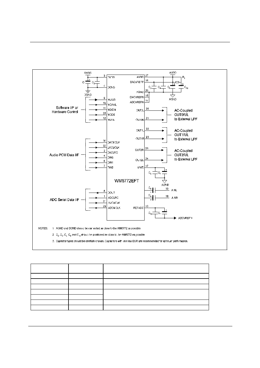
WM8772EFT ≠ 32 PIN TQFP
Production Data
w
PD Rev 4.1 October 2004
66
APPLICATIONS INFORMATION
RECOMMENDED EXTERNAL COMPONENTS
RECOMMENDED EXTERNAL COMPONENTS VALUES
COMPONENT
REFERENCE
SUGGESTED
VALUE
DESCRIPTION
C1 and C5
10
µ
F
De-coupling for DVDD and AVDD.
C2 to C4
0.1
µ
F
De-coupling for DVDD and AVDD.
C8 and C9
1
µ
F
Analogue input high pass filter capacitors
C6 and C10
0.1
µ
F
C7 and C11
10
µ
F
Reference de-coupling capacitors for VMID and ADCREF pin.
C12 10
µ
F
Filtering for VREFP. Omit if AVDD low noise.
R1 330
Filtering for VREP. Use 0
if AVDD low noise.
Table 23 External Components Description
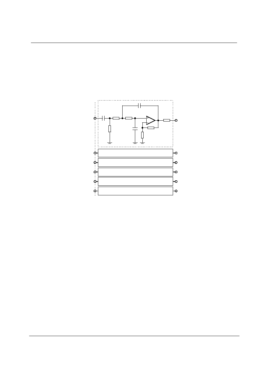
Production Data
WM8772EFT ≠ 32 PIN TQFP
w
PD Rev 4.1 October 2004
67
SUGGESTED ANALOGUE LOW PASS POST DAC FILTERS
It is recommended that a lowpass filter be applied to the output from each DAC channel for Hi Fi applications. Typically a
second order filter is suitable and provides sufficient attenuation of high frequency components (the unique low order, high
bit count multi-bit sigma delta DAC structure used in WM8772EFT produces much less high frequency output noise than
normal sigma delta DACs. This filter is typically also used to provide the 2x gain needed to provide the standard 2Vrms
output level from most consumer equipment.
Figure 51 shows a suitable post DAC filter circuit, with 2x gain. Alternative inverting filter architectures might also be used
with as good results.
7.5k
1.8k
10uF
1.0nF
10k
4.7k
680pF
4.7k
51
OP_FIL
VOUT1L
OP_FIL
VOUT1R
OP_FIL
VOUT2R
OP_FIL
VOUT2L
OP_FIL
VOUT3L
OP_FIL
VOUT3R
Figure 51 Recommended Post DAC Filter Circuit
WM8772EFT ≠ 32 PIN TQFP
Production Data
w
PD Rev 4.1 October 2004
68
To ensure that system `pop' noise is kept to a minimum when power is applied or removed, a
transistor clamp circuit arrangement may be added to the output connectors of the system. A
recommended clamp circuit configuration is shown below.
Figure 52 Output Clamp Circuit
When the +VS power supply is applied, PNP transistor Q10 of the trigger circuit is held on until
capacitor C49 is fully charged. With transistor Q10 held `on', NPN transistors Q4 to Q9 of the clamp
circuits are also switched on holding the system outputs near to GND. When capacitor C49 is fully
charged transistors Q10 and Q4 to Q9 are switched off setting the outputs active.
When the +VS power supply is removed, PNP transistor Q11 of the trigger circuit is switched on. In
turn, transistors Q4 to Q9 of the clamp circuits are switched on holding the outputs of the evaluation
board near to GND until the rest of the circuitry on the board has settled.
Note: It is recommended that low Vce
sat
switching transistors should be used in this circuit to ensure
that the clamp is applied before the rest of the circuitry has time to power down.
Important: If a trigger circuit such as the one shown is to be used, it is important that the +VS
supply drops quicker than any other supply to ensure that the outputs are clamped during the
period when `pop' noise may occur.

Production Data
WM8772EFT ≠ 32 PIN TQFP
w
PD Rev 4.1 October 2004
69
PACKAGE DIMENSIONS
NOTES:
A. ALL LINEAR DIMENSIONS ARE IN MILLIMETERS.
B. THIS DRAWING IS SUBJECT TO CHANGE WITHOUT NOTICE.
C. BODY DIMENSIONS DO NOT INCLUDE MOLD FLASH OR PROTRUSION, NOT TO EXCEED 0.25MM.
D. MEETS JEDEC.95 MS-026, VARIATION = ABA. REFER TO THIS SPECIFICATION FOR FURTHER DETAILS.
Symbols
Dimensions
(mm)
MIN
NOM
MAX
A
----- ----- 1.20
A
1
0.05 ----- 0.15
A
2
0.95 1.00 1.05
b
0.30 0.37 0.45
c
0.09 ----- 0.20
D
9.00 BSC
D
1
7.00 BSC
E
9.00 BSC
E
1
7.00 BSC
e
0.80 BSC
L
0.45 0.60 0.75
0
o
3.5
o
7
o
Tolerances of Form and Position
ccc
0.10
REF:
JEDEC.95, MS-026
DM028.A
FT: 32 PIN TQFP (7 x 7 x 1.0 mm)
17
24
8
1
D1
D
E1
E
9
16
25
32
b
e
c
L
A
A2
A1
SEATING PLANE
ccc C
-C-

WM8772EFT ≠ 32 PIN TQFP
Production Data
w
PD Rev 4.1 October 2004
70
IMPORTANT NOTICE
Wolfson Microelectronics plc (WM) reserve the right to make changes to their products or to discontinue any product or
service without notice, and advise customers to obtain the latest version of relevant information to verify, before placing
orders, that information being relied on is current. All products are sold subject to the WM terms and conditions of sale
supplied at the time of order acknowledgement, including those pertaining to warranty, patent infringement, and limitation
of liability.
WM warrants performance of its products to the specifications applicable at the time of sale in accordance with WM's
standard warranty. Testing and other quality control techniques are utilised to the extent WM deems necessary to support
this warranty. Specific testing of all parameters of each device is not necessarily performed, except those mandated by
government requirements.
In order to minimise risks associated with customer applications, adequate design and operating safeguards must be used
by the customer to minimise inherent or procedural hazards. Wolfson products are not authorised for use as critical
components in life support devices or systems without the express written approval of an officer of the company. Life
support devices or systems are devices or systems that are intended for surgical implant into the body, or support or
sustain life, and whose failure to perform when properly used in accordance with instructions for use provided, can be
reasonably expected to result in a significant injury to the user. A critical component is any component of a life support
device or system whose failure to perform can be reasonably expected to cause the failure of the life support device or
system, or to affect its safety or effectiveness.
WM assumes no liability for applications assistance or customer product design. WM does not warrant or represent that
any license, either express or implied, is granted under any patent right, copyright, mask work right, or other intellectual
property right of WM covering or relating to any combination, machine, or process in which such products or services might
be or are used. WM's publication of information regarding any third party's products or services does not constitute WM's
approval, license, warranty or endorsement thereof.
Reproduction of information from the WM web site or datasheets is permissible only if reproduction is without alteration and
is accompanied by all associated warranties, conditions, limitations and notices. Representation or reproduction of this
information with alteration voids all warranties provided for an associated WM product or service, is an unfair and deceptive
business practice, and WM is not responsible nor liable for any such use.
Resale of WM's products or services with statements different from or beyond the parameters stated by WM for that
product or service voids all express and any implied warranties for the associated WM product or service, is an unfair and
deceptive business practice, and WM is not responsible nor liable for any such use.
ADDRESS:
Wolfson Microelectronics plc
26 Westfield Road
Edinburgh
EH11 2QB
United Kingdom
Tel :: +44 (0)131 272 7000
Fax :: +44 (0)131 272 7001
Email ::
sales@wolfsonmicro.com