Document Outline
- WM8773
- 24-bit, 96kHz ADC with 8 Channel I/P Multiplexer
- DESCRIPTION
- FEATURES
- APPLICATIONS
- BLOCK DIAGRAM
- PIN CONFIGURATION
- ORDERING INFORMATION
- PIN DESCRIPTION
- ABSOLUTE MAXIMUM RATINGS
- RECOMMENDED OPERATING CONDITIONS
- ELECTRICAL CHARACTERISTICS
- TERMINOLOGY
- MASTER CLOCK TIMING
- DIGITAL AUDIO INTERFACE Ö MASTER MODE
- DIGITAL AUDIO INTERFACE Ö SLAVE MODE
- MPU INTERFACE TIMING
- DEVICE DESCRIPTION
- INTRODUCTION
- AUDIO DATA SAMPLING RATES
- POWERDOWN MODES
- DIGITAL AUDIO INTERFACE
- CONTROL INTERFACE OPERATION
- CONTROL INTERFACE REGISTERS
- REGISTER MAP
- DIGITAL FILTER CHARACTERISTICS
- ADC FILTER RESPONSES
- ADC HIGH PASS FILTER
- EXTERNAL CIRCUIT CONFIGURATION
- PACKAGE DIMENSIONS
- IMPORTANT NOTICE
- REVISION HISTORY

WM8773
24-bit, 96kHz ADC with 8 Channel I/P Multiplexer
WOLFSON MICROELECTRONICS LTD
w :: www.wolfsonmicro.com
Product Preview, April 2002, Rev 1.0
Copyright
2002 Wolfson Microelectronics Ltd.
DESCRIPTION
The WM8773 is a high performance, stereo audio ADC with
an 8 channel input selector. The WM8773 is ideal for
digitising multiple analogue sources for surround sound
processing applications for home hi-fi, automotive and other
audio visual equipment.
A stereo 24-bit multi-bit sigma delta ADC is used with an
eight stereo channel input selector. Each channel has
analogue domain mute and programmable gain control.
Digital audio output word lengths from 16-32 bits and
sampling rates from 8kHz to 96kHz are supported.
The audio data interface supports I
2
S, left justified, right
justified and DSP digital audio formats.
The device is controlled via a 3 wire serial interface. The
interface provides access to all features including channel
selection, volume controls, mutes, de-emphasis and power
management facilities. The device is available in a 64-pin
TQFP package.
FEATURES
∑
Audio
Performance
-
102dB SNR (`A' weighted @ 48kHz) ADC
∑
ADC Sampling Frequency: 8kHz ≠ 96kHz
∑
3-Wire SPI MPU Serial Control Interface
∑
Master or Slave Clocking Mode
∑
Programmable Audio Data Interface Modes
-
I
2
S, Left, Right Justified or DSP
-
16/20/24/32 bit Word Lengths
∑
Analogue Record Monitor Outputs
∑
Eight stereo ADC inputs with analogue gain adjust from
+19dB to ≠12dB in 1dB steps
∑
2.7V to 5.5V Analogue, 2.7V to 3.6V Digital supply
Operation
∑
5V tolerant digital inputs
APPLICATIONS
∑
Surround Sound AV Processors and Hi-Fi systems
∑
Automotive
Audio
BLOCK DIAGRAM
STEREO
ADC
A
G
ND1
AVD
D
1
VM
I
D
A
D
C
AUDIO INTERFACE
AND
DIGITAL FILTERS
I
N
PU
T
SO
U
R
C
E SE
L
E
C
T
OR
AIN2R
AIN3L
AIN3R
AIN4L
AIN4R
AIN5L
AIN5R
AIN6L
AIN6R
RECL
RECR
AINOPR
AINOPL
AI
N
V
GR
AI
N
V
G
L
RE
F
A
DC
DV
DD
DG
ND
CONTROL INTERFACE
DI
CE
CL
RE
S
E
TB
AIN2L
AIN1R
AIN1L
AIN7L
AIN7R
AIN8L
AIN8R
WM8773
MUTE
ADCLRC
BCLK
DOUT
MCLK

WM8773
Product Preview
PP Rev 1.0 June 2002
2
PIN CONFIGURATION
ORDERING INFORMATION
DEVICE TEMP.
RANGE
PACKAGE
WM8773IFT/V
-40 to +85
o
C 64-pin
TQFP
AV
DD1
V
M
I
DADC
AG
ND1
NC
AI
NO
P
R
AI
NV
G
L
AI
NV
G
R
RE
CL
RE
CR
AIN1L
AIN4L
AIN3R
AIN3L
AIN2R
AIN2L
AIN1R
AIN4R
AIN5L
AIN6L
RE
S
E
TB
BCL
K
MC
L
K
CL
DI
CE
NC
NC
NC
NC
ADCL
RC
NC
NC
NC
NC
NC
NC
NC
NC
NC
1
9
8
7
6
5
4
3
2
11
10
21 22 23 24 25 26 27
18 19 20
41
40
39
38
37
36
43
42
64 63 62 61 60 59 58
17
57 56 55 54
35
34
33
AI
NO
P
L
AIN5R
RE
FADC
NC
NC
DV
DD
DO
UT
NC
53 52 51 50 49
NC
NC
NC
NC
NC
NC
AVDD2
NC
NC
AIN6R
AIN7L
AIN7R
AIN8R
14
13
12
16
15
AIN8L
NC
28 29 30 31 32
46
45
44
48
47
AGND2
DGND

Product Preview
WM8773
PP Rev 1.0 June 2002
3
PIN DESCRIPTION
PIN NAME TYPE
DESCRIPTION
1 AIN1L
Analogue
Input
Channel 1 left input multiplexor virtual ground
2 AIN1R
Analogue
Input
Channel 1 right input multiplexor virtual ground
3 AIN2L
Analogue
Input
Channel 2 left input multiplexor virtual ground
4 AIN2R
Analogue
Input
Channel 2 right input multiplexor virtual ground
5 AIN3L
Analogue
Input
Channel 3 left input multiplexor virtual ground
6 AIN3R
Analogue
Input
Channel 3 right input multiplexor virtual ground
7 AIN4L
Analogue
Input
Channel 4 left input multiplexor virtual ground
8 AIN4R
Analogue
Input
Channel 4 right input multiplexor virtual ground
9 AIN5L
Analogue
Input
Channel 5 left input multiplexor virtual ground
10 AIN5R
Analogue
Input
Channel 5 right input multiplexor virtual ground
11 AIN6L
Analogue
Input
Channel 6 left input multiplexor virtual ground
12 AIN6R
Analogue
Input
Channel 6 right input multiplexor virtual ground
13 AIN7L
Analogue
Input
Channel 7 left input multiplexor virtual ground
14 AIN7R
Analogue
Input
Channel 7 right input multiplexor virtual ground
15 AIN8L
Analogue
Input
Channel 8 left input multiplexor virtual ground
16 AIN8R
Analogue
Input
Channel 8 right input multiplexor virtual ground
17 AINOPL
Analogue
Output
Left channel multiplexor output
18 AINVGL
Analogue
Input
Left channel multiplexor virtual ground
19 AINVGR
Analogue
Input
Right channel multiplexor virtual ground
20 AINOPR
Analogue
Output
Right channel multiplexor output
21 RECL
Analogue
Output
Left channel input mux select output
22 RECR
Analogue
Output
Right channel input mux select output
23 REFADC
Analogue
Output
ADC reference buffer decoupling pin; 10uF external decoupling
24 VMIDADC
Analogue
Output
ADC midrail divider decoupling pin; 10uF external decoupling
25 AGND1 Supply
Analogue negative supply and substrate connection
26 AVDD1 Supply
Analogue positive supply
27
NC
No connection
28
NC
No connection
29
NC
No connection
30
NC
No connection
31
NC
No connection
32
NC
No connection
33 AVDD2 Supply
Analogue positive supply
34
NC
No connection
35
NC
No connection
36
NC
No connection
37
NC
No connection
38
NC
No connection
39
NC
No connection
40
NC
No connection
41
NC
No connection
42
NC
No connection
43
NC
No connection
44
NC
No connection
45
NC
No connection
46
NC
No connection
47 AGND2 Supply
Analogue negative supply and substrate connection
48 DGND Supply
Digital negative supply
49 DVDD Supply
Digital positive supply

WM8773
Product Preview
PP Rev 1.0 June 2002
4
PIN NAME TYPE
DESCRIPTION
50
NC
No connection
51
NC
No connection
52 DOUT
Digital
output
ADC data output
53
NC
No connection
54
NC
No connection
55
NC
No connection
56
NC
No connection
57
NC
No connection
58 ADCLRC
Digital
input/output
ADC left/right word clock
59 BCLK
Digital
input/output
ADC audio interface bit clock
60 MCLK
Digital
input
Master ADC clock; 256, 384, 512 or 768fs (fs = word clock frequency)
61 CL
Digital
input
Serial interface clock (5V tolerant)
62 DI
Digital
input
Serial interface data (5V tolerant)
63 CE
Digital
input
Serial interface Latch signal (5V tolerant)
64 RESETB
Digital
input
Device reset input (resets gain stages to 0dB)
(5V tolerant)
Note : Digital input pins have Schmitt trigger input buffers and are 5V tolerant.

Product Preview
WM8773
PP Rev 1.0 June 2002
5
ABSOLUTE MAXIMUM RATINGS
Absolute Maximum Ratings are stress ratings only. Permanent damage to the device may be caused by continuously operating at
or beyond these limits. Device functional operating limits and guaranteed performance specifications are given under Electrical
Characteristics at the test conditions specified.
ESD Sensitive Device. This device is manufactured on a CMOS process. It is therefore generically susceptible
to damage from excessive static voltages. Proper ESD precautions must be taken during handling and storage
of this device.
CONDITION
MIN MAX
Digital supply voltage
-0.3V
+3.63V
Analogue supply voltage
-0.3V +7V
Voltage range digital inputs (DI, CL, CE & RESETB)
DGND -0.3V
+7V
Voltage range digital inputs (MCLK, ADCLRC & BCLK)
DGND -0.3V
DVDD + 0.3V
Voltage range analogue inputs
AGND -0.3V
AVDD +0.3V
Master Clock Frequency
37MHz
Operating temperature range, T
A
-40
∞
C +85
∞
C
Storage temperature
-65
∞
C +150
∞
C
Package body temperature (soldering 10 seconds)
+240
∞
C
Package body temperature (soldering 2 minutes)
+183
∞
C
Notes:
1.
Analogue and digital grounds must always be within 0.3V of each other.
WM8773
Product Preview
PP Rev 1.0 June 2002
6
RECOMMENDED OPERATING CONDITIONS
PARAMETER SYMBOL
TEST
CONDITIONS
MIN
TYP
MAX
UNIT
Digital supply range
DVDD
2.7
3.6
V
Analogue supply range
AVDD
2.7
5.5
V
Ground
AGND, DGND
0
V
Difference DGND to AGND
-0.3
0
+0.3
V
Note: Digital supply DVDD must never be more than 0.3V greater than AVDD.
ELECTRICAL CHARACTERISTICS
Test Conditions
AVDD = 5V, DVDD = 3.3V, AGND = 0V, DGND = 0V, T
A
= +25
o
C, fs = 48kHz, MCLK = 256fs unless otherwise stated.
PARAMETER SYMBOL
TEST
CONDITIONS
MIN
TYP
MAX
UNIT
Digital Logic Levels (TTL Levels)
Input LOW level
V
IL
0.8
V
Input HIGH level
V
IH
2.0
V
Output LOW
V
OL
I
OL
=1mA
0.1 x DVDD
V
Output HIGH
V
OH
I
OH
-1mA
0.9 x DVDD
V
Analogue Reference Levels
Reference voltage
V
VMID
AVDD/2
≠
50mV
AVDD/2 AVDD/2
+
50mV
V
Potential divider resistance
R
VMID
AVDD to VMIDADC
and VMIDADC to
AGND
40k 50k 60k
Ohms
ADC Performance
Input Signal Level (0dB)
1.0
x
AVDD/5
Vrms
SNR (Note 1,2)
A-weighted, 0dB gain
@ fs = 48kHz
93 102 dB
SNR (Note 1,2)
A-weighted, 0dB gain
@ fs = 96kHz
98 dB
Dynamic Range (note 2)
A-weighted, -60dB
full scale input
102 dB
kHz, 0dBFs -90 -80 dB
Total Harmonic Distortion (THD)
1kHz, -3dBFs
-95
-85
dB
ADC Channel Separation
1kHz Input
90
dB
Programmable Gain Step Size
0.5 1.0 1.5 dB
Programmable Gain Range
1kHz Input
-12
+19
dB
Mute Attenuation
1kHz Input, 0dB gain
97
dB
1kHz 100mVpp
50
dB
Power Supply Rejection Ratio
PSRR
20Hz to 20kHz
100mVpp
45 dB
Product Preview
WM8773
PP Rev 1.0 June 2002
7
Test Conditions
AVDD = 5V, DVDD = 3.3V, AGND = 0V, DGND = 0V, T
A
= +25
o
C, fs = 48kHz, MCLK = 256fs unless otherwise stated.
PARAMETER SYMBOL
TEST
CONDITIONS
MIN
TYP
MAX
UNIT
Analogue input (AIN) to Analogue output (VOUT) (Load=10k ohms, 50pF, gain = 0dB) Record Monitor Output
0dB Full scale output voltage
1.0 x
AVDD/5
Vrms
SNR (Note 1)
90
100
dB
1kHz,
0dB -90 dB
THD
1kHz,
-3dB -95 dB
1kHz
100mVpp
50 dB
Power Supply Rejection Ratio
PSRR
20Hz to 20kHz
100mVpp
45 dB
Mute Attenuation (REC Output
Only)
1kHz,
0dB 100 dB
Supply Current
Analogue supply current
AVDD = 5V
100
mA
Digital supply current
DVDD
=
3.3V 20
mA
Notes:
1.
Ratio of output level with 1kHz full scale input, to the output level with all zeros into the digital input, measured `A'
weighted.
2.
All performance measurements done with 20kHz low pass filter, and where noted an A-weight filter. Failure to use
such a filter will result in higher THD+N and lower SNR and Dynamic Range readings than are found in the Electrical
Characteristics. The low pass filter removes out of band noise; although it is not audible it may affect dynamic
specification values.
3.
VMID decoupled with 10uF and 0.1uF capacitors (smaller values may result in reduced performance).
TERMINOLOGY
1.
Signal-to-noise ratio (dB) - SNR is a measure of the difference in level between the full scale output and the output
with no signal applied. (No Auto-zero or Automute function is employed in achieving these results).
2.
Dynamic range (dB) - DNR is a measure of the difference between the highest and lowest portions of a signal.
Normally a THD+N measurement at 60dB below full scale. The measured signal is then corrected by adding the 60dB
to it. (e.g. THD+N @ -60dB= -32dB, DR= 92dB).
3.
THD+N (dB) - THD+N is a ratio, of the rms values, of (Noise + Distortion)/Signal.
4.
Stop band attenuation (dB) - Is the degree to which the frequency spectrum is attenuated (outside audio band).
5.
Channel Separation (dB) - Also known as Cross-Talk. This is a measure of the amount one channel is isolated from
the other. Normally measured by sending a full scale signal down one channel and measuring the other.
6.
Pass-Band Ripple - Any variation of the frequency response in the pass-band region.

WM8773
Product Preview
PP Rev 1.0 June 2002
8
MASTER CLOCK TIMING
MCLK
t
MCLKL
t
MCLKH
t
MCLKY
Figure 1 Master Clock Timing Requirements
Test Conditions
AVDD = 5V, DVDD = 3.3V, AGND = 0V, AGND, DGND = 0V, T
A
= +25
o
C, fs = 48kHz, MCLK = 256fs unless otherwise stated.
PARAMETER SYMBOL
TEST
CONDITIONS
MIN
TYP
MAX
UNIT
System Clock Timing Information
MCLK System clock pulse width high
t
MCLKH
11
ns
MCLK System clock pulse width low
t
MCLKL
11
ns
MCLK System clock cycle time
t
MCLKY
28
ns
MCLK Duty cycle
40:60 60:40
Table 1 Master Clock Timing Requirements
DIGITAL AUDIO INTERFACE ≠ MASTER MODE
BCLK
DOUT
ADCLRC
WM8773
ADC
DSP/
ENCODER/
DECODER
Figure 2 Audio Interface - Master Mode
Product Preview
WM8773
PP Rev 1.0 June 2002
9
BCLK
(Output)
DOUT
ADCLRC
t
DL
t
DDA
Figure 3 Digital Audio Data Timing ≠ Master Mode
Test Conditions
AVDD = 5V, DVDD = 3.3V, AGND, DGND = 0V, T
A
= +25
o
C, Master Mode, fs = 48kHz, MCLK = 256fs unless otherwise stated.
PARAMETER SYMBOL
TEST
CONDITIONS
MIN
TYP
MAX
UNIT
Audio Data Input Timing Information
ADCLRC propagation delay
from BCLK falling edge
t
DL
0
10
ns
DOUT propagation delay
from BCLK falling edge
t
DDA
0
10
ns
Table 2 Digital Audio Data Timing ≠ Master Mode
DIGITAL AUDIO INTERFACE ≠ SLAVE MODE
BCLK
DOUT
ADCLRC
WM8773
CODEC
DSP
ENCODER/
DECODER
Figure 4 Audio Interface ≠ Slave Mode

WM8773
Product Preview
PP Rev 1.0 June 2002
10
BCLK
ADCLRC
t
BCH
t
BCL
t
BCY
DOUT
t
DD
Figure 5 Digital Audio Data Timing ≠ Slave Mode
Test Conditions
AVDD = 5V, DVDD = 3.3V, AGND = 0V, DGND = 0V, T
A
= +25
o
C, Slave Mode, fs = 48kHz, MCLK = 256fs unless otherwise
stated.
PARAMETER SYMBOL
TEST
CONDITIONS
MIN
TYP
MAX
UNIT
Audio Data Input Timing Information
BCLK cycle time
t
BCY
50
ns
BCLK pulse width high
t
BCH
20
ns
BCLK pulse width low
t
BCL
20
ns
DOUT propagation delay
from BCLK falling edge
t
DD
0
10
ns
Table 3 Digital Audio Data Timing ≠ Slave Mode
Note:
1.
ADCLRC should be synchronous with MCLK, although the WM8773 interface is tolerant of phase variations or jitter on
these signals.

Product Preview
WM8773
PP Rev 1.0 June 2002
11
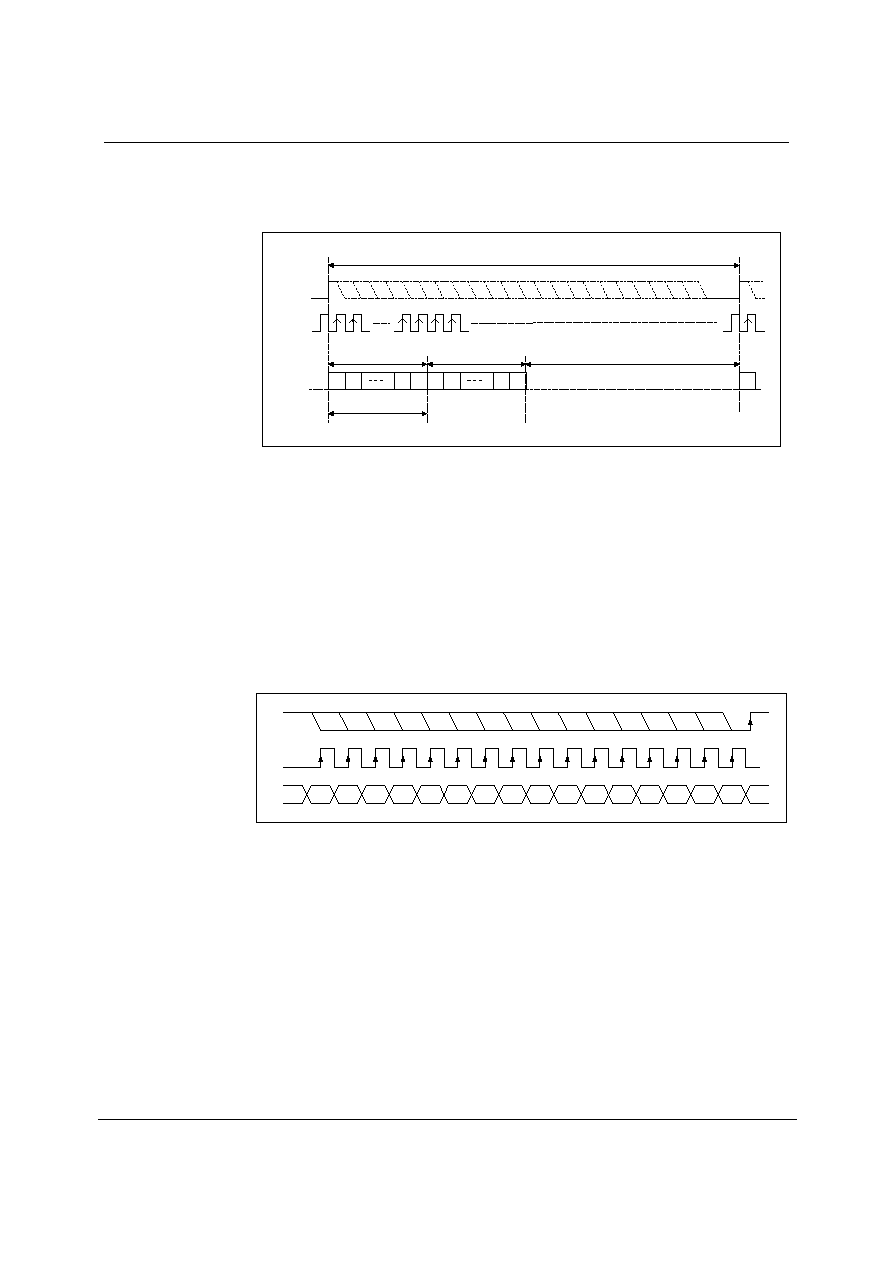
MPU INTERFACE TIMING
t
RCHO
t
RCSU
CE
CL
DI
t
CSL
t
DHO
t
DSU
t
CSH
t
SCY
t
SCH
t
SCL
t
SCS
LSB
t
CSS
RESETB
Figure 6 SPI compatible Control Interface Input Timing
Test Conditions
AVDD = 5V, DVDD = 3.3V, AGND, DGND = 0V, T
A
= +25
o
C, fs = 48kHz, MCLK = 256fs unless otherwise stated
PARAMETER SYMBOL
MIN
TYP
MAX
UNIT
CE to RESETB hold time
t
RCSU
20
ns
RESETB to CL setup time
t
RCHO
20
ns
CL rising edge to CE rising edge
t
SCS
60
ns
CL pulse cycle time
t
SCY
80
ns
CL pulse width low
t
SCL
30
ns
CL pulse width high
t
SCH
30
ns
DI to CL set-up time
t
DSU
20
ns
CL to DI hold time
t
DHO
20
ns
CE pulse width low
t
CSL
20
ns
CE pulse width high
t
CSH
20
ns
CE rising to CL rising
t
CSS
20
ns
Table 4 3-wire SPI compatible Control Interface Input Timing Information

WM8773
Product Preview
PP Rev 1.0 June 2002
12
DEVICE DESCRIPTION
INTRODUCTION
WM8773 is a complete stereo audio ADC with 8-channel multiplexed input.
The input multiplexor to the ADC is configured to allow large signal levels to be input to the ADC,
using external resistors to reduce the amplitude of larger signals to within the normal operating range
of the ADC. The ADC input PGA also allows input signals to be gained up to +19dB and attenuated
down to -12dB. This allows the user maximum flexibility in the use of the ADC.
Analogue record monitor outputs are also available, to allow stereo analogue signals from any of the
8 stereo inputs to be sent to sent to one of the two stereo outputs. This allows the user to monitor
the signal that is being digitised either prior to the input programmable gain amplifier (PGA) or after
gain has been applied. It is intended that the RECL/R outputs are only used to drive a high
impedance buffer.
The Audio Interface may be configured to operate in either master or slave mode. In Slave mode
ADCLRC and BCLK are both inputs. In Master mode ADCLRC and BCLK are all outputs.
Control of internal functionality of the device is by 3-wire serial control interface. The control interface
may be asynchronous to the audio data interface as control data will be re-synchronised to the audio
processing internally. CE, CL, DI and RESETB are 5V tolerant with TTL input thresholds, allowing
the WM8773 to used with DVDD = 3.3V and be controlled by a controller with 5V output.
Operation using system clock of 256fs, 384fs, 512fs or 768fs is provided. In Slave mode selection
between clock rates is automatically controlled. In master mode the master clock to sample rate ratio
is set by control bit ADCRATE. Sample rates (fs) from less than 8ks/s up to 96ks/s are allowed,
provided the appropriate system clock is input.
The audio data interface supports right, left and I
2
S interface formats along with a highly flexible DSP
serial port interface.
AUDIO DATA SAMPLING RATES
In a typical digital audio system there is only one central clock source producing a reference clock to
which all audio data processing is synchronised. This clock is often referred to as the audio system's
Master Clock. The external master system clock can be applied directly through the MCLK input pin
with no software configuration necessary. In a system where there are a number of possible sources
for the reference clock it is recommended that the clock source with the lowest jitter be used to
optimise the performance of the ADC.
The master clock for WM8773 supports ADC audio sampling rates from 256fs to 768fs, where fs is
the audio sampling frequency (ADCLRC) typically 32kHz, 44.1kHz, 48kHz or 96kHz. The master
clock is used to operate the digital filters and the noise shaping circuits.
In Slave mode the WM8773 has a master detection circuit that automatically determines the
relationship between the master clock frequency and the sampling rate (to within +/- 32 system
clocks). If there is a greater than 32 clocks error the interface is disabled and maintains the output
level at the last sample. The master clock must be synchronised with ADCLRC, although the
WM8773 is tolerant of phase variations or jitter on this clock. Table 5 shows the typical master clock
frequency inputs for the WM8773.
The signal processing for the WM8773 typically operates at an oversampling rate of 128fs for the
ADC. For ADC operation at 96kHz, it is recommended that the user set the ADCOSR bit. This
changes the ADC signal processing oversample rate to 64fs.
System Clock Frequency (MHz)
SAMPLING
RATE
(ADCLRC)
256fs 384fs 512fs 768fs
32kHz 8.192
12.288
16.384
24.576
44.1kHz 11.2896
16.9340
22.5792
33.8688
48kHz 12.288
18.432
24.576
36.864
Table 5 System Clock Frequencies Versus Sampling Rate
Product Preview
WM8773
PP Rev 1.0 June 2002
13
In Master mode BCLK and ADCLRC are generated by the WM8773. The frequency of ADCLRC is
determined by setting the required ratio of MCLK to ADCLRC using the ADCRATE control bits (Table
6).
ADCRATE[2:0] MCLK:ADCLRC
RATIO
010 256fs
011 384fs
100 512fs
101 768fs
Table 6 Master Mode MCLK:ADCLRC ratio select
Table 7 shows the settings for ADCRATE for common sample rates and MCLK frequencies.
System Clock Frequency (MHz)
256fs 384fs 512fs 768fs
SAMPLING
RATE
ADCLRC
ADCRATE
=010
ADCRATE
=011
ADCRATE
=100
ADCRATE
=101
32kHz 8.192
12.288
16.384
24.576
44.1kHz 11.2896 16.9340 22.5792 33.8688
48kHz 12.288 18.432 24.576 36.864
96kHz 24.576
36.864
Unavailable
Unavailable
Table 7 Master Mode ADC frequency selection
BCLK is also generated by the WM8773. The frequency of BCLK depends on the mode of operation.
In 256/384/512fs modes (ADCRATE=010 or 011, 100 or 101) BCLK = MCLK/4. However if DSP
mode is selected as the audio interface mode then BCLK=MCLK.
POWERDOWN MODES
The WM8773 has powerdown control bits allowing specific parts of the WM8773 to be powered off
when not being used. The 8-channel input source selector and input buffer may be powered down
using control bit AINPD. When AINPD is set all inputs to the source selector (AIN1l/R to AIN8L/R)
are switched to a buffered VMIDADC. Control bit ADCPD powers off the ADC and also the ADC input
PGAs. Setting AINPD and ADCPD will powerdown everything except the references VMIDADC and
ADCREF. These may be powered down by setting PDWN. Setting PDWN will override all other
powerdown control bits. It is recommended that the 8-channel input mux and buffer and ADC are
powered down before setting PDWN. The default is for all powerdown bits to be set except PDWN.
The Powerdown control bits allow parts of the device to be powered down when not in use.
DIGITAL AUDIO INTERFACE
MASTER AND SLAVE MODES
The audio interface operates in either Slave or Master mode, selectable using the MS control bit. In
both Master and Slave modes, ADCDAT is always an output. The default is Slave mode.
In Slave mode (MS=0) ADCLRC and BCLK are inputs to the WM8773 (Figure 7). ADCLRC is
sampled by the WM8773 on the rising edge of BCLK. ADC data is output on DOUT and changes on
the falling edge of BCLK. By setting control bit BCLKINV the polarity of BCLK may be reversed so
that ADCLRC is sampled on the falling edge of BCLK and DOUT changes on the rising edge of
BCLK.

WM8773
Product Preview
PP Rev 1.0 June 2002
14
BCLK
DOUT
ADCLRC
WM8773
CODEC
DSP
ENCODER/
DECODER
Figure 7 Slave Mode
In Master mode (MS=1) ADCLRC and BCLK are outputs from the WM8773 (Figure 8). ADCLRC and
BITCLK are generated by the WM8773. ADCDAT is output on DOUT and changes on the falling
edge of BCLK. By setting control bit BCLKINV the polarity of BCLK may be reversed so that DOUT
changes on the rising edge of BCLK.
BCLK
DOUT
ADCLRC
WM8773
ADC
DSP/
ENCODER/
DECODER
Figure 8 Master Mode
AUDIO INTERFACE FORMATS
Audio data is output from the ADC filters, via the Digital Audio Interface. 5 popular interface formats
are supported:
∑
Left Justified mode
∑
Right Justified mode
∑
I
2
S mode
∑
DSP
Early
mode
∑
DSP Late mode
All 5 formats send the MSB first and support word lengths of 16, 20, 24 and 32 bits, with the
exception of 32 bit right justified mode, which is not supported.
In left justified, right justified and I
2
S modes, the digital audio interface outputs ADC data on DOUT.
Audio Data for each stereo channel is time multiplexed with ADCLRC indicating whether the left or
right channel is present. ADCLRC is also used as a timing reference to indicate the beginning or end
of the data words.
In left justified, right justified and I
2
S modes, the minimum number of BCLKs per ADCLRC period is 2
times the selected word length. ADCLRC must be high for a minimum of word length BCLKs and
low for a minimum of word length BCLKs. Any mark to space ratio on ADCLRC is acceptable
provided the above requirements are met.

Product Preview
WM8773
PP Rev 1.0 June 2002
15
The ADC data may also be output in DSP early or late modes, with ADCLRC used as a frame sync
to identify the MSB of the first word. The minimum number of BCLKs per ADCLRC period is 2 times
the selected word length
LEFT JUSTIFIED MODE
In left justified mode, the MSB of the ADC data is output on DOUT and changes on the same falling
edge of BCLK as ADCLRC and may be sampled on the rising edge of BCLK. ADCLRC is high
during the left samples and low during the right samples (Figure 9).
LEFT CHANNEL
RIGHT CHANNEL
ADCLRC
BCLK
DOUT
1/fs
n
3
2
1
n-2 n-1
LSB
MSB
n
3
2
1
n-2 n-1
LSB
MSB
Figure 9 Left Justified Mode TIming Diagram
RIGHT JUSTIFIED MODE
In right justified mode, the LSB of the ADC data is output on DOUT and changes on the
falling edge of BCLK preceding an ADCLRC transition and may be sampled on the rising
edge of BCLK. ADCLRC is high during the left samples and low during the right samples).
LEFT CHANNEL
RIGHT CHANNEL
ADCLRC
BCLK
DOUT
1/fs
n
3
2
1
n-2 n-1
LSB
MSB
n
3
2
1
n-2 n-1
LSB
MSB
Figure 10 Right Justified Mode TIming Diagram

WM8773
Product Preview
PP Rev 1.0 June 2002
16
I
2
S MODE
In I
2
S mode, the MSB of the ADC data is output on DOUT and changes on the first falling edge of
BCLK following an ADCLRC transition and may be sampled on the rising edge of BCLK. ADCLRC is
low during the left samples and high during the right samples.
LEFT CHANNEL
RIGHT CHANNEL
ADCLRC
BCLK
DOUT
1/fs
n
3
2
1
n-2 n-1
LSB
MSB
n
3
2
1
n-2 n-1
LSB
MSB
1 BCLK
1 BCLK
Figure 11 I
2
S Mode TIming Diagram
DSP EARLY MODE
The MSB of the left channel ADC data is output on DOUT and changes on the first falling edge of
BCLK following a low to high ADCLRC transition and may be sampled on the rising edge of BCLK.
The right channel ADC data is contiguous with the left channel data (Figure 12)
ADCLRC
BCK
DOUT
Word Length (WL)
1/fs
LEFT CHANNEL
n
2
1
n-1
LSB
MSB
n
2
1
n-1
RIGHT CHANNEL
NO VALID DATA
1 BCLK
1 BCLK
Figure 12 DSP Early Mode Timing Diagram ≠ ADC Data Output
Product Preview
WM8773
PP Rev 1.0 June 2002
17
DSP LATE MODE
The MSB of the left channel ADC data is output on DOUT and changes on the same falling edge of
BCLK as the low to high ADCLRC transition and may be sampled on the rising edge of BCLK. The
right channel ADC data is contiguous with the left channel data (Figure 13).
ADCLRC
BCK
DOUT
Word Length (WL)
1/fs
LEFT CHANNEL
n
2
1
n-1
LSB
MSB
n
2
1
n-1
RIGHT CHANNEL
NO VALID DATA
1
Figure 13 DSP Late Mode Timing Diagram ≠ ADC Data Output
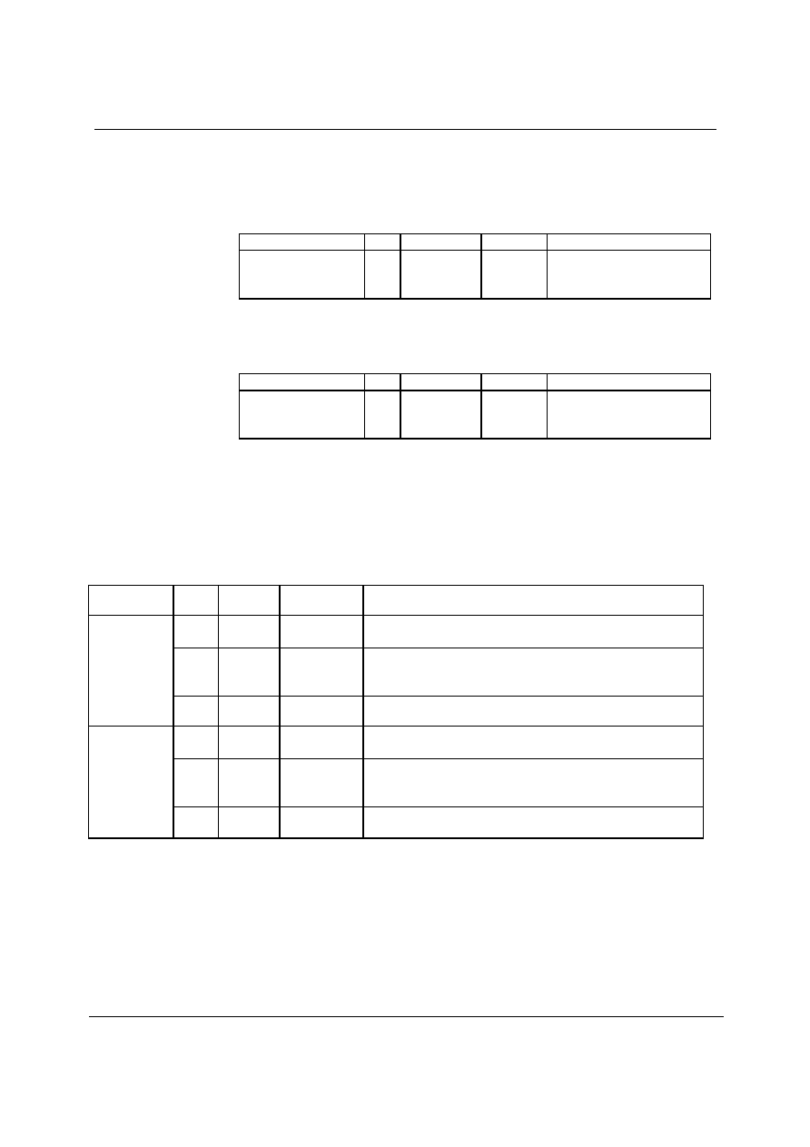
CONTROL INTERFACE OPERATION
The WM8773 is controlled using a 3-wire SPI compatible serial configuration.
The control interface is 5V tolerant, meaning that the control interface input signals CE, CL and DI
may have an input high level of 5V while DVDD is 3V. Input thresholds are determined by DVDD.
RESETB is also 5V tolerant.
3-WIRE (SPI COMPATIBLE) SERIAL CONTROL MODE
DI is used for the program data, CL is used to clock in the program data and CE is used to latch the
program data. DI is sampled on the rising edge of CL. The 3-wire interface protocol is shown in
Figure 14.
Figure 14 3-wire SPI compatible Interface
Note:
1.
B[15:9] are Control Address Bits
2.
B[8:0] are Control Data Bits
3.
CE is edge sensitive ≠ the data is latched on the rising edge of CE.
B15 B14 B13 B12 B11 B10 B9 B8 B7 B6 B5 B4 B3 B2 B1 B0
CE
CL
DI

WM8773
Product Preview
PP Rev 1.0 June 2002
18
CONTROL INTERFACE REGISTERS
DIGITAL AUDIO INTERFACE CONTROL REGISTER
Interface format is selected via the FMT[1:0] register bits:
REGISTER ADDRESS
BIT
LABEL
DEFAULT
DESCRIPTION
10110
Interface Control
1:0
FMT[1:0]
10
Interface format Select
00 : right justified mode
01: left justified mode
10: I
2
S mode
11: DSP (early or late) mode
In left justified, right justified or I
2
S modes, the LRP register bit controls the polarity of ADCLRC. If
this bit is set high, the expected polarity of ADCLRC will be the opposite of that shown Figure 9, and.
Note that if this feature is used as a means of swapping the left and right channels, a 1 sample
phase difference will be introduced. In DSP modes, the LRP register bit is used to select between
early and late modes.
REGISTER ADDRESS
BIT
LABEL
DEFAULT
DESCRIPTION
In left/right/I
2
S modes:
ADCLRC Polarity (normal)
0 : normal ADCLRC polarity
1: inverted ADCLRC polarity
10110
Interface Control
2 LRP
0
In DSP mode:
0 : Early DSP mode
1: Late DSP mode
By default, ADCLRC is sampled on the rising edge of BCLK and should ideally change on the falling
edge. Data sources that change ADCLRC on the rising edge of BCLK can be supported by setting
the BCP register bit. Setting BCP to 1 inverts the polarity of BCLK to the inverse of that shown in
Figure 9, Figure 10, Figure 11, Figure 12, and Figure 13.
REGISTER ADDRESS
BIT
LABEL
DEFAULT
DESCRIPTION
10110
Interface Control
3
BCP
0
BCLK Polarity (DSP modes)
0 : normal BCLK polarity
1: inverted BCLK polarity
The WL[1:0] bits are used to control the word length.
REGISTER ADDRESS
BIT
LABEL
DEFAULT
DESCRIPTION
10110
Interface Control
5:4 WL[1:0]
10
Word
Length
00 : 16 bit data
01: 20 bit data
10: 24 bit data
11: 32 bit data
Note:
1.
If 32-bit mode is selected in right justified mode, the WM8773 defaults to 24 bits.
2.
In 24 bit I
2
S mode, any width of 24 bits or less is supported provided that ADCLRC is high for a
minimum of 24 BCLKs and low for a minimum of 24 BCLKs.

Product Preview
WM8773
PP Rev 1.0 June 2002
19
Control bit MS selects between audio interface Master and Slave Modes. In Master mode ADCLRC
and BCLK are outputs and are generated by the WM8773. In Slave mode ADCLRC and BCLK are
inputs to WM8773.
REGISTER ADDRESS
BIT
LABEL
DEFAULT
DESCRIPTION
10111
Interface Control
8
MS
0
Audio Interface Master/Slave Mode
select:
0 : Slave Mode
1: Master Mode
MASTER MODE ADCLRC FREQUENCY SELECT
In Master mode the WM8773 generates ADCLRC and BCLK. These clocks are derived from master
clock and the ratio of MCLK to ADCLRC and are set by ADCRATE.
REGISTER ADDRESS
BIT
LABEL
DEFAULT
DESCRIPTION
0111 ADCLRC frequency
select
2:0 ADCRATE[2:0]
010
Master
Mode
MCLK:ADCLRC
ratio select:
010: 256fs
011: 384fs
100: 512fs
101: 768fs
ADC OVERSAMPLING RATE SELECT
For ADC operation at 96kHz it is recommended that the user set the ADCOSR bit. This changes the
ADC signal processing oversample rate to 64fs.
REGISTER ADDRESS
BIT
LABEL
DEFAULT
DESCRIPTION
10111
ADC Oversampling Rate
3
ADCOSR
0
ADC oversampling rate select
0: 128x oversampling
1: 64x oversampling
MUTE MODES
Each ADC channel has an individual mute control bit, which mutes the input to the ADC. In addition
both channels may be muted by setting ADCMUTE.
REGISTER ADDRESS
BIT
LABEL
DEFAULT
DESCRIPTION
11001
ADC Mute
7
ADCMUTE
0
ADC MUTE Left and Right
0 : Normal Operation
1: mute ADC left and ADC
right
11001
ADC Mute Left
5 MUTE
0 ADC
Mute
select
0 : Normal Operation
1: mute ADC left
11010
ADC Mute Right
5 MUTE
0 ADC
Mute
select
0 : Normal Operation
1: mute ADC right
The Record outputs may be enabled by setting RECEN, where RECEN enables the RECL and
RECR outputs.
REGISTER ADDRESS
BIT
LABEL
DEFAULT
DESCRIPTION
10100
REC Enable
5
RECEN
0
REC Output Enable
0 : REC output muted
1: REC output enabled
WM8773
Product Preview
PP Rev 1.0 June 2002
20
POWERDOWN MODE AND ADC DISABLE
Setting the PDWN register bit immediately powers down the WM8773, including the references,
overriding all other powerdown control bits. All trace of the previous input samples are removed, but
all control register settings are preserved. When PDWN is cleared the digital filters will be
reinitialised. It is recommended that the 8-channel input mux and buffer, and ADC are powered down
before setting PDWN.
REGISTER ADDRESS
BIT
LABEL
DEFAULT
DESCRIPTION
11000
Powerdown Control
0
PDWN
0
Power Down Mode Select:
0 : Normal Mode
1: Power Down Mode
The ADC may also be powered down by setting the ADCD disable bit. Setting ADCD will disable the
ADC and select a low power mode. The ADC digital filters will be reset and will reinitialise when
ADCD is reset.
REGISTER ADDRESS
BIT
LABEL
DEFAULT
DESCRIPTION
11000
ADC Powerdown Control
1 ADCD
1 ADC
Disable:
0 : Normal Mode
1: Power Down Mode
ADC GAIN CONTROL
Control bits LAG[4:0] and RAG[4:0] control the ADC input gain, allowing the user to attenuate the
ADC input signal to match the full-scale range of the ADC. The gain is independently adjustable on
left and right inputs. Left and right inputs may also be independently muted. The LRBOTH control bit
allows the user to write the same attenuation value to both left and right volume control registers. The
ADC volume and mute also applies to the bypass signal path.
REGISTER
ADDRESS
BIT LABEL DEFAULT
DESCRIPTION
4:0
LAG[4:0] 01100
(0dB)
Attenuation data for Left channel ADC gain in 1dB steps. See Table
8
5
MUTE 0
Mute for Left channel ADC:
0: Mute off
1: Mute on
11001
Attenuation
ADCL
6
LRBOTH 0 Setting LRBOTH will write the same gain value to LAG[4:0] and
RAG[4:0]
4:0
RAG[4:0] 01100
(0dB)
Attenuation data for right channel ADC gain in 1dB steps. See Table
8
5
MUTE 0
Mute for Right channel ADC:
0: Mute off
1: Mute on
11010
Attenuation
ADCR
6
LRBOTH 0 Setting LRBOTH will write the same gain value to RAG[4:0] and
LAG[4:0]
Product Preview
WM8773
PP Rev 1.0 June 2002
21
ADC INPUT GAIN
Registers LAG and RAG control the left and right channel gain into the stereo ADC in 1dB steps from
+19dB to ≠12dB Table 8 shows how the attenuation levels are selected from the 5-bit words.
L/RAG[6:0] ATTENUATION
LEVEL
0 -12dB
: :
01100 0dB
: :
11111 +19dB
Table 8 ADC Gain Control
ADC HIGHPASS FILTER DISABLE
The ADC digital filters contain a digital highpass filter. This defaults to enabled and can be disabled
using software control bit ADCHPD.
REGISTER ADDRESS
BIT
LABEL
DEFAULT
DESCRIPTION
10110
ADC control
8
ADCHPD
0
ADC Highpass filter disable:
0: Highpass filter enabled
1: Highpass filter disabled
ADC INPUT MUX AND POWERDOWN CONTROL
REGISTER
ADDRESS
BIT LABEL
DEFAULT
DESCRIPTION
2:0
LMX[2:0] 000
ADC left channel input mux control
bits (see Table 9)
6:4
RMX[2:0] 000
ADC right channel input mux
control bits (see Table 9)
11011
ADC mux and
powerdown
control
8
AINPD 1 Input mux and buffer powerdown
0: Input mux and buffer
enabled
1: Input mux and buffer
powered down
Register bits LMX and RMX control the left and right channel inputs into the stereo ADC. The default
is AIN1. However if the analogue input buffer is powered down, by setting AINPD, then all 8-channel
mux inputs are switched to buffered VMIDADC.
LMX[2:0] LEFT
ADC
INPUT
RMX[2:0]
RIGHT ADC INPUT
000 AIN1L 000 AIN1R
001 AIN2L 001 AIN2R
010 AIN3L 010 AIN3R
011 AIN4L 011 AIN4R
100 AIN5L 100 AIN5R
101 AIN6L 101 AIN6R
110 AIN7L 110 AIN7R
111 AIN8L 111 AIN8R
Table 9 ADC Input Mux Control

WM8773
Product Preview
PP Rev 1.0 June 2002
22
SOFTWARE REGISTER RESET
Writing to register 11111 will cause a register reset, resetting all register bits to their default
values.
REGISTER MAP
The complete register map is shown below. The detailed description can be found in the relevant text of the device description. The
WM8773 can be configured using the Control Interface. All unused bits should be set to `0'.
REGISTER B15 B14 B13 B12 B11 B10 B9 B8
B7
B6
B5
B4 B3
B2
B1 B0 DEFAULT
R20(14h)
0
0
1
0
1
0
0
x x
x
RECEN
x
x
x
x
x
000000000
R22(16h)
0
0
1
0
1
1
0
ADCHPD x
x
WL[1:0] BCP
LRP
FMT[1:0]
000100010
R23(17h)
0
0
1
0
1
1
1
MS x x
x
x
ADCOSR ADCRATE[2:0] 000010010
R24(18h)
0
0
1
1
0
0
0
x x
x
x
x
x
x
ADCD
PWDN
000111110
R25(19h)
0
0
1
1
0
0
1
x ADCMUTE
LRBOT
H
MUTE LAG[4:0]
000001100
R26(1Ah)
0
0
1
1
0
1
0
x x
LRBOT
H
MUTE RAG[4:0]
000001100
R27(1Bh)
0
0
1
1
0
1
1
AINPD x
RMX[2:0]
x
LMX[2:0] 100000000
R31(1Fh)
0
0
1
1
1
1
1
RESET not
reset
ADDRESS
DATA DEFAULT
Product Preview
WM8773
PP Rev 1.0 June 2002
23
REGISTER
ADDRESS
BIT LABEL DEFAULT
DESCRIPTION
10100
Mute
5
RECEN
0
REC Output Enable
0 : REC output muted
1: REC output enabled
1:0 FMT[1:0]
10
Interface format select
00: right justified mode
01: left justified mode
10: I
2
S mode
11: DSP mode
ADCLRC Polarity or DSP Early/Late mode select
2 LRP
0
Left Justified / Right Justified /
I
2
S
0: Standard ADCLRC Polarity
1: Inverted ADCLRC Polarity
DSP Mode
0: Early DSP mode
1: Late DSP mode
3 BCP
0
BITCLK
Polarity
0: Normal - ADCLRC sampled on rising edge of BCLK;
DOUT changes on falling edge of BCLK.
1: Inverted - ADCLRC sampled on falling edge of BCLK;
DOUT changes on rising edge of BCLK.
5:4 WL[1:0]
10 Input
Word
Length
00: 16-bit Mode
01: 20-bit Mode
10: 24-bit Mode
11: 32-bit Mode (not supported in right justified mode)
10110
Interface
Control
8
ADCHPD
0
ADC Highpass Filter Disable:
0: Highpass Filter enabled
1: Highpass Filter disabled
2:0 ADCRATE[2:0]
010
Master Mode MCLK:ADCLRC ratio select:
010: 256fs
011: 384fs
100: 512fs
3 ADCOSR
0 ADC oversample rate select
0: 128x oversampling
1: 64x oversampling
10111
Master Mode
control
8
MS
0
Maser/Slave interface mode select
0: Slave Mode ≠ ADCLRC and BCLK are inputs
1: Master Mode ≠ ADCLRC and BCLK are outputs
0
PWDN
0
Chip Powerdown Control (works in together with ADCD)
0: All circuits running, outputs are active
1: All circuits in power save mode, outputs muted
11000
Powerdown
Control
1 ADCD
1
ADC
powerdown:
0: ADC enabled
1: ADC disabled
4:0 LAG[4:0] 01100
(0dB)
Attenuation data for left channel ADC gain in 1dB steps
5
MUTE
0
Mute for Left channel ADC:
0: Mute off
1: Mute on
6
LRBOTH
0
Setting LRBOTH will write the same gain value to LAG[4:0] and
RAG[4:0]
11001
Attenuation
ADCL
7
ADCMUTE
0
Mute for Left and Right channel ADC:
0: Mute off
1: Mute on

WM8773
Product Preview
PP Rev 1.0 June 2002
24
REGISTER
ADDRESS
BIT LABEL DEFAULT
DESCRIPTION
4:0 RAG[4:0] 01100
(0dB)
Attenuation data for right channel ADC gain in 1dB steps
5
MUTE
0
Mute for Right channel ADC:
0: Mute off
1: Mute on
11010
Attenuation
ADCR
6
LRBOTH
0
Setting LRBOTH will write the same gain value to RAG[4:0] and
LAG[4:0]
2:0
LMX[2:0]
000
ADC left channel input mux control bits
6:4
RMX[2:0]
000
ADC right channel input mux control bits
11011
ADC mux
control
8
AINPD
1
Input mux and buffer powerdown
0: Input mux and buffer enabled
1: Input mux and buffer powered down
11111
Software reset
[8:0]
RESET
Not reset
Writing to this register will apply a reset to the device registers.
Table 10 Register Map Description
Product Preview
WM8773
PP Rev 1.0 June 2002
25
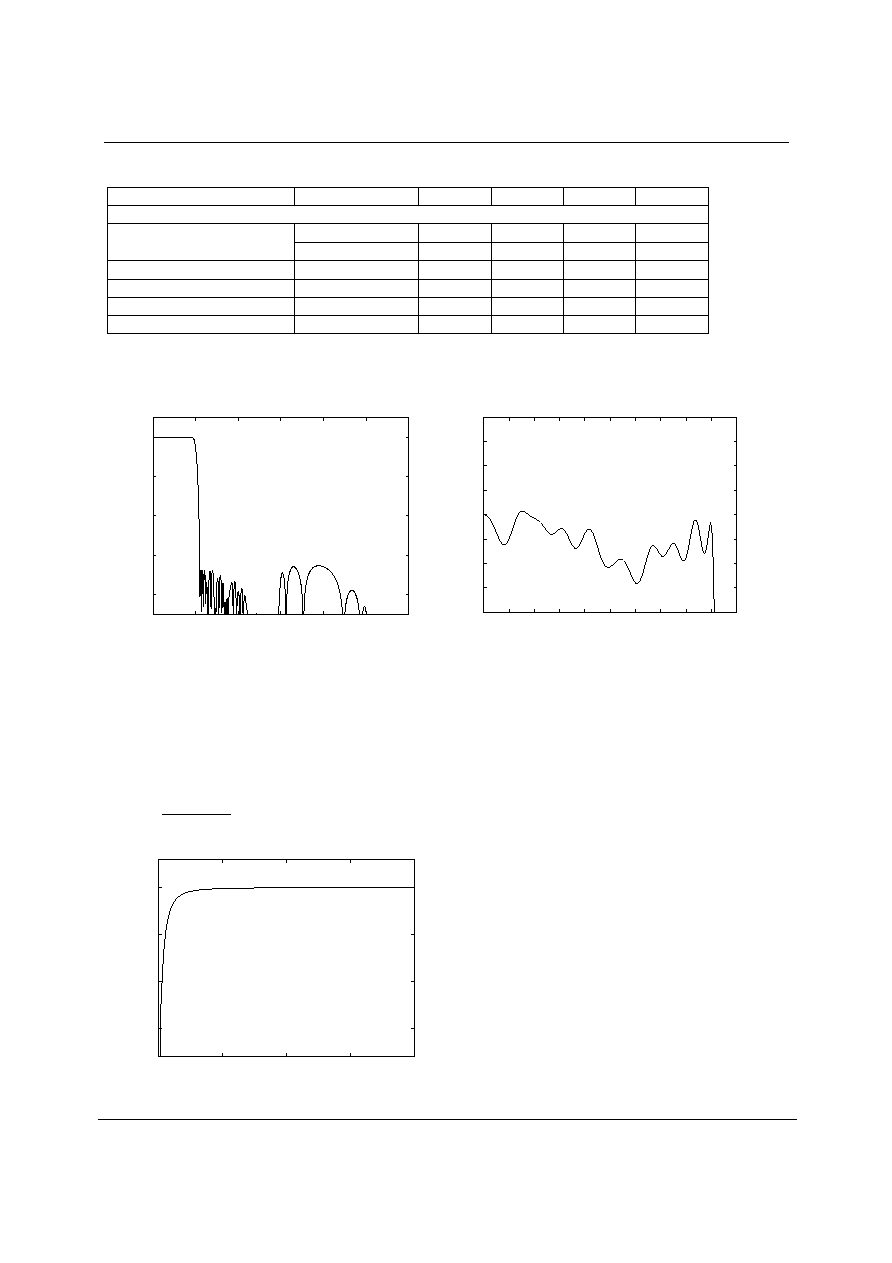
DIGITAL FILTER CHARACTERISTICS
PARAMETER TEST
CONDITIONS
MIN
TYP
MAX
UNIT
ADC Filter
±
0.01 dB
0
0.4535fs
Passband
-6dB
0.5fs
Passband ripple
±
0.01 dB
Stopband
0.5465fs
Stopband Attenuation
f > 0.5465fs
-65
dB
Group Delay
22
fs
Table 11 Digital Filter Characteristics
ADC FILTER RESPONSES
-80
-60
-40
-20
0
0
0.5
1
1.5
2
2.5
3
Response (dB)
Frequency (Fs)
Figure 15 ADC Digital Filter Frequency Response
-0.02
-0.015
-0.01
-0.005
0
0.005
0.01
0.015
0.02
0
0.05
0.1
0.15
0.2
0.25
0.3
0.35
0.4
0.45
0.5
Response (dB)
Frequency (Fs)
Figure 16 ADC Digital Filter Ripple
ADC HIGH PASS FILTER
The WM8773 has a selectable digital highpass filter to remove DC offsets. The filter response is characterised by the
following polynomial.
Figure 17 ADC Highpass Filter Response
1 - z
-1
1 - 0.9995z
-1
H(z) =
-15
-10
-5
0
0
0.0005
0.001
0.0015
0.002
Response (dB)
Frequency (Fs)

WM8773
Product Preview
PP Rev 1.0 June 2002
26
AIN1L
10K
10uF
AIN2L
10K
10uF
AIN3L
10K
10uF
AIN7L
10K
10uF
AIN8L
10K
10uF
AIN1R
10K
10uF
AIN2R
10K
10uF
AIN3R
10K
10uF
AIN7R
10K
10uF
AIN8R
10K
10uF
SOURCE
SELECTOR
INPUTS
AINVGR
AINOPR
5K
AINVGL
AINOPL
5K
EXTERNAL CIRCUIT CONFIGURATION
In order to allow the use of 2V rms and larger inputs to the ADC inputs, a structure is used that uses
external resistors to drop these larger voltages. This also increases the robustness of the circuit to
external abuse such as ESD pulse.
Figure 18 shows the ADC input multiplexor circuit with external components allowing 2Vrms inputs to
be applied.
Figure 18 ADC Input Multiplexor Configuration

Product Preview
WM8773
PP Rev 1.0 June 2002
27
PACKAGE DIMENSIONS
DM027.A
FT: 64 PIN TQFP (10 x 10 x 1.0 mm)
4
c
L
SEATING PLANE
A2
A
A1
ccc
C
-C-
e
33
b
16
D1
E1
17
64
49
48
E
D
NOTES:
A. ALL LINEAR DIMENSIONS ARE IN MILLIMETERS.
B. THIS DRAWING IS SUBJECT TO CHANGE WITHOUT NOTICE.
C. BODY DIMENSIONS DO NOT INCLUDE MOLD FLASH OR PROTRUSION, NOT TO EXCEED 0.25MM.
D. MEETS JEDEC.95 MS-026, VARIATION = ACD. REFER TO THIS SPECIFICATION FOR FURTHER DETAILS.
Symbols
Dimensions
(mm)
MIN
NOM
MAX
A
-----
-----
1.20
A
1
0.05
-----
0.15
A
2
1.00
b
0.22
c
-----
0.20
D
12.00 BSC
D
1
10.00 BSC
E
12.00 BSC
E
1
10.00 BSC
e
0.50 BSC
L
0.60
4
0
o
3.5
o
7
o
Tolerances of Form and Position
ccc
0.08
REF:
JEDEC.95, MS-026
0.95
0.17
0.09
0.27
1.05
0.45
0.75
1
32

WM8773
Product Preview
PP Rev 1.0 June 2002
28
IMPORTANT NOTICE
Wolfson Microelectronics Ltd (WM) reserve the right to make changes to their products or to discontinue any product or
service without notice, and advise customers to obtain the latest version of relevant information to verify, before placing
orders, that information being relied on is current. All products are sold subject to the WM terms and conditions of sale
supplied at the time of order acknowledgement, including those pertaining to warranty, patent infringement, and limitation
of liability.
WM warrants performance of its products to the specifications applicable at the time of sale in accordance with WM's
standard warranty. Testing and other quality control techniques are utilised to the extent WM deems necessary to support
this warranty. Specific testing of all parameters of each device is not necessarily performed, except those mandated by
government requirements.
In order to minimise risks associated with customer applications, adequate design and operating safeguards must be used
by the customer to minimise inherent or procedural hazards.
WM assumes no liability for applications assistance or customer product design. WM does not warrant or represent that
any license, either express or implied, is granted under any patent right, copyright, mask work right, or other intellectual
property right of WM covering or relating to any combination, machine, or process in which such products or services might
be or are used. WM's publication of information regarding any third party's products or services does not constitute WM's
approval, license, warranty or endorsement thereof.
Reproduction of information from the WM web site or datasheets is permissible only if reproduction is without alteration and
is accompanied by all associated warranties, conditions, limitations and notices. Representation or reproduction of this
information with alteration voids all warranties provided for an associated WM product or service, is an unfair and deceptive
business practice, and WM is neither responsible nor liable for any such use.
Resale of WM's products or services with statements different from or beyond the parameters stated by WM for that
product or service voids all express and any implied warranties for the associated WM product or service, is an unfair and
deceptive business practice, and WM is not responsible nor liable for any such use.
ADDRESS:
Wolfson Microelectronics Ltd
20 Bernard Terrace
Edinburgh
EH8 9NX
United Kingdom
Tel :: +44 (0)131 272 7000
Fax :: +44 (0)131 272 7001
Email :: sales@wolfsonmicro.com

Product Preview
WM8773
PP Rev 1.0 June 2002
29
REVISION HISTORY
DATE REV
ORIGINATOR
CHANGES