 | –≠–ª–µ–∫—Ç—Ä–æ–Ω–Ω—ã–π –∫–æ–º–ø–æ–Ω–µ–Ω—Ç: WM8775 | –°–∫–∞—á–∞—Ç—å:  PDF PDF  ZIP ZIP |
Document Outline
- WM8775
- 24-bit,96kHz ADC with 4 Channel I/P Multiplexer
- DESCRIPTION
- FEATURES
- APPLICATIONS
- BLOCK DIAGRAM
- TABLE OF CONTENTS
- PIN CONFIGURATION
- ORDERING INFORMATION
- PIN DESCRIPTION
- ABSOLUTE MAXIMUM RATINGS
- RECOMMENDED OPERATING CONDITIONS
- ELECTRICAL CHARACTERISTICS
- MASTER CLOCK TIMING
- DIGITAL AUDIO INTERFACE Ö MASTER MODE
- DIGITAL AUDIO INTERFACE Ö SLAVE MODE
- 3-WIRE MPU INTERFACE TIMING
- 2-WIRE MPU INTERFACE TIMING
- DEVICE DESCRIPTION
- INTRODUCTION
- AUDIO DATA SAMPLING RATES
- POWERDOWN MODES
- POWER-ON-RESET
- DIGITAL AUDIO INTERFACE
- CONTROL INTERFACE OPERATION
- CONTROL INTERFACE REGISTERS
- LIMITER /AUTOMATIC LEVEL CONTROL (ALC)
- REGISTER MAP
- DIGITAL FILTER CHARACTERISTICS
- ADC FILTER RESPONSES
- ADC HIGH PASS FILTER
- APPLICATIONS INFORMATION
- EXTERNAL CIRCUIT CONFIGURATION
- RECOMMENDED EXTERNAL COMPONENTS
- PACKAGE DIMENSIONS
- IMPORTANT NOTICE
- ADDRESS:

w
WM8775
24-bit, 96kHz ADC with 4 Channel I/P Multiplexer
WOLFSON MICROELECTRONICS plc
w :: www.wolfsonmicro.com
Product Preview, June 2004, Rev 1.8
Copyright
2004 Wolfson Microelectronics plc
DESCRIPTION
The WM8775 is a high performance, stereo audio ADC
with a 4 channel input mixer. The WM8775 is ideal for
digitising multiple analogue sources for surround sound
processing applications for home hi-fi, automotive and
other audio visual equipment.
A stereo 24-bit multi-bit sigma delta ADC is used with a
four stereo channel input selector. Each channel has
programmable gain control. Digital audio output word
lengths from 16-32 bits and sampling rates from 32kHz
to 96kHz are supported.
The audio data interface supports I
2
S, left justified, right
justified and DSP digital audio formats.
The device is controlled via a 2 or 3 wire serial interface.
The interface provides access to all features including
channel selection, volume controls, mutes, de-emphasis
and power management facilities.
The device is available in a 28-pin SSOP package. The
WM8775 is software compatible with the WM8776.
FEATURES
∑
Audio Performance
-
102dB SNR (`A' weighted @ 48kHz)
-
-90dB THD
∑
ADC Sampling Frequency: 32kHz ≠ 96kHz
∑
Four stereo ADC inputs with analogue gain adjust from
+24dB to ≠21dB in 0.5dB steps
∑
Digital gain adjust from -21.5dB to -103dB.
∑
Programmable Automatic Level Control (ALC) or Limiter on
ADC input
∑
3-Wire SPI Compatible or 2-wire Serial Control Interface
∑
Master or Slave Clocking Mode
∑
Programmable Audio Data Interface Modes
-
I
2
S, Left, Right Justified or DSP
-
16/20/24/32 bit Word Lengths
∑
2.7V to 5.5V Analogue, 2.7V to 3.6V Digital supply Operation
∑
5V tolerant digital inputs
APPLICATIONS
∑ Surround Sound AV Processors and Hi-Fi systems
∑ Automotive Audio
BLOCK DIAGRAM
AG
N
D
AVD
D
VMI
D
A
D
C
AUDIO INTERFACE
AND
DIGITAL FILTERS
A
DCR
E
F
P
DV
DD
DG
ND
CONTROL INTERFACE
DI
CE
CL
W
WM8775
ADCLRC
BCLK
DOUT
MCLK
A
DCR
E
F
G
N
D
STEREO
ADC
ALC
AIN2R
AIN3L
AIN3R
AIN4L
AIN4R
AINOPR
AINOPL
AINVGR
AINVGL
AIN2L
AIN1R
AIN1L
I
N
PU
T
MI
XER
VMID
MO
D
E

WM8775
Product Preview
w
PP Rev 1.8, June 2004
2
TABLE OF CONTENTS
DESCRIPTION ................................................................................................................1
FEATURES......................................................................................................................1
BLOCK DIAGRAM ..........................................................................................................1
PIN CONFIGURATION....................................................................................................3
ORDERING INFORMATION ...........................................................................................3
PIN DESCRIPTION .........................................................................................................4
ABSOLUTE MAXIMUM RATINGS ..................................................................................5
RECOMMENDED OPERATING CONDITIONS ..............................................................5
ELECTRICAL CHARACTERISTICS ...............................................................................6
TERMINOLOGY ......................................................................................................................7
MASTER CLOCK TIMING...............................................................................................7
DIGITAL AUDIO INTERFACE ≠ MASTER MODE ...................................................................7
DIGITAL AUDIO INTERFACE ≠ SLAVE MODE ......................................................................8
3-WIRE MPU INTERFACE TIMING ......................................................................................10
2-WIRE MPU INTERFACE TIMING ......................................................................................10
DEVICE DESCRIPTION ................................................................................................12
INTRODUCTION ...................................................................................................................12
AUDIO DATA SAMPLING RATES.........................................................................................12
POWERDOWN MODES .......................................................................................................13
POWER-ON-RESET .............................................................................................................14
DIGITAL AUDIO INTERFACE ...............................................................................................15
CONTROL INTERFACE OPERATION ..................................................................................18
CONTROL INTERFACE REGISTERS ..................................................................................19
LIMITER / AUTOMATIC LEVEL CONTROL (ALC) ................................................................23
REGISTER MAP ...................................................................................................................28
DIGITAL FILTER CHARACTERISTICS ........................................................................32
ADC FILTER RESPONSES...................................................................................................32
ADC HIGH PASS FILTER .....................................................................................................32
APPLICATIONS INFORMATION ..................................................................................33
EXTERNAL CIRCUIT CONFIGURATION .............................................................................33
RECOMMENDED EXTERNAL COMPONENTS ....................................................................34
IMPORTANT NOTICE ...................................................................................................36
ADDRESS: ............................................................................................................................36
Product Preview
WM8775
w
PP Rev 1.8, June 2004
3
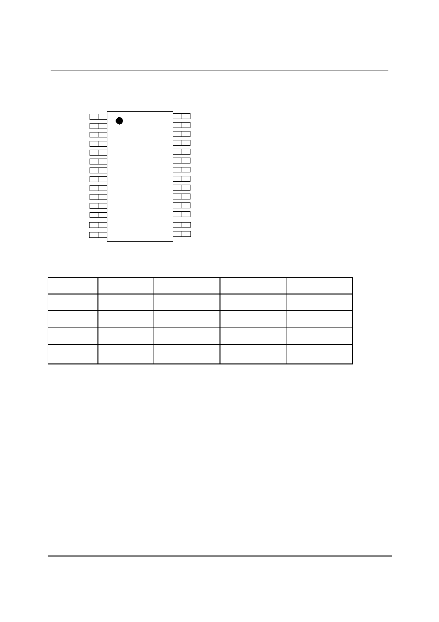
PIN CONFIGURATION
AVDD
VMIDADC
AGND
AINOPL
AINVGL
AINVGR
AIN1R
AIN4L
AIN3R
AIN3L
AIN2R
AIN2L
AIN1L
AIN4R
BCLK
ADCLRC
DOUT
MCLK
CE
1
9
8
7
6
5
4
3
2
11
10
13
14
15
16
17
18
19
28
27
26
25
ADCREFGND
CL
MODE
12
20
21
22
23
24
DI
ADCREFP
DGND
DVDD
AINOPR
NC
ORDERING INFORMATION
DEVICE
TEMP. RANGE
PACKAGE
MOISTURE
SENSITIVITY LEVEL
PEAK SOLDERING
TEMP
WM8775EDS
-25 to +85
o
C
28-pin SSOP
MSL1
240
∞C
WM8775EDS/R
-25 to +85
o
C
28-pin SSOP
(tape and reel)
MSL1
240
∞C
WM8775SEDS
-25 to +85
o
C
28-pin SSOP
(lead free)
MSL1
260
∞C
WM8775SEDS/R
-25 to +85
o
C
28-pin SSOP
(lead free, tape and reel)
MSL1
260
∞C
Note:
Reel quantity = 2,000
WM8775
Product Preview
w
PP Rev 1.8, June 2004
4
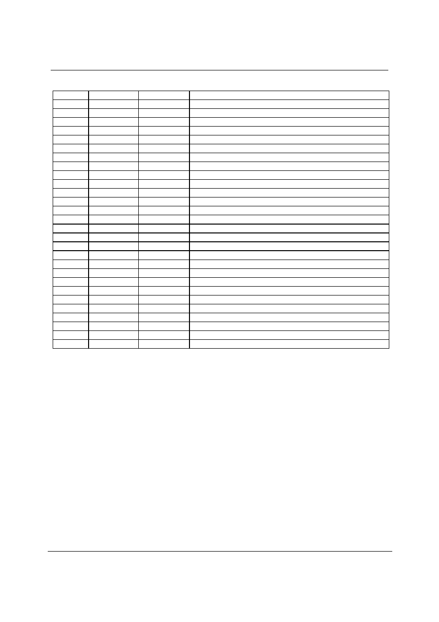
PIN DESCRIPTION
PIN
NAME
TYPE
DESCRIPTION
1
AIN1L
Analogue Input
Channel 1 left input multiplexor virtual ground
2
BCLK
Digital input/output ADC audio interface bit clock
3
MCLK
Digital input
Master ADC clock; 256, 384, 512 or 768fs (fs = word clock frequency)
4
DOUT
Digital output
ADC data output
5
ADCLRC
Digital input/output ADC left/right word clock
6
DGND
Supply
Digital negative supply
7
DVDD
Supply
Digital positive supply
8
MODE
Digital Input
Serial Interface Mode select (5V tolerant)
9
CE
Digital Input
Serial Interface Latch signal (5V tolerant)
10
DI
Digital input/output Serial interface data (5V tolerant)
11
CL
Digital input
Serial interface clock (5V tolerant)
12
NC
No connection
13
VMIDADC
Analogue Output
ADC midrail divider decoupling pin; 10uF external decoupling
14
ADCREFGND
Supply
ADC negative supply and substrate connection
15
ADCREFP
Analogue Output
ADC positive reference decoupling pin; 10uF external decoupling
16
AVDD
Supply
Analogue positive supply
17
AGND
Supply
Analogue negative supply and substrate connection
18
AINVGR
Analogue Input
Right channel multiplexor virtual ground
19
AINOPR
Analogue Output
Right channel multiplexor output
20
AINVGL
Analogue Input
Left channel multiplexor virtual ground
21
AINOPL
Analogue Output
Left channel multiplexor output
22
AIN4R
Analogue Input
Channel 4 right input multiplexor virtual ground
23
AIN4L
Analogue Input
Channel 4 left input multiplexor virtual ground
24
AIN3R
Analogue Input
Channel 3 right input multiplexor virtual ground
25
AIN3L
Analogue Input
Channel 3 left input multiplexor virtual ground
26
AIN2R
Analogue Input
Channel 2 right input multiplexor virtual ground
27
AIN2L
Analogue Input
Channel 2 left input multiplexor virtual ground
28
AIN1R
Analogue Input
Channel 1 right input multiplexor virtual ground
Note : Digital input pins have Schmitt trigger input buffers and pins 8, 9, 10 and 11 are 5V tolerant.
Product Preview
WM8775
w
PP Rev 1.8, June 2004
5
ABSOLUTE MAXIMUM RATINGS
Absolute Maximum Ratings are stress ratings only. Permanent damage to the device may be caused by continuously operating at
or beyond these limits. Device functional operating limits and guaranteed performance specifications are given under Electrical
Characteristics at the test conditions specified.
ESD Sensitive Device. This device is manufactured on a CMOS process. It is therefore generically susceptible
to damage from excessive static voltages. Proper ESD precautions must be taken during handling and storage
of this device.
Wolfson tests its package types according to IPC/JEDEC J-STD-020B for Moisture Sensitivity to determine acceptable storage
conditions prior to surface mount assembly. These levels are:
MSL1 = unlimited floor life at <30
∞C / 85% Relative Humidity. Not normally stored in moisture barrier bag.
MSL2 = out of bag storage for 1 year at <30
∞C / 60% Relative Humidity. Supplied in moisture barrier bag.
MSL3 = out of bag storage for 168 hours at <30
∞C / 60% Relative Humidity. Supplied in moisture barrier bag.
CONDITION
MIN
MAX
Digital supply voltage
-0.3V
+3.63V
Analogue supply voltage
-0.3V
+7V
Voltage range digital inputs (DI, CL, CE and MODE)
DGND -0.3V
+7V
Voltage range digital inputs (MCLK, ADCLRC and BCLK)
DGND -0.3V
DVDD + 0.3V
Voltage range analogue inputs
AGND -0.3V
AVDD +0.3V
Master Clock Frequency
37MHz
Operating temperature range, T
A
-25
∞C
+85
∞C
Storage temperature
-65
∞C
+150
∞C
Notes:
1.
Analogue and digital grounds must always be within 0.3V of each other.
RECOMMENDED OPERATING CONDITIONS
PARAMETER
SYMBOL
TEST CONDITIONS
MIN
TYP
MAX
UNIT
Digital supply range
DVDD
2.7
3.6
V
Analogue supply range
AVDD
2.7
5.5
V
Ground
AGND, DGND
0
V
Difference DGND to AGND
-0.3
0
+0.3
V
Note: Digital supply DVDD must never be more than 0.3V greater than AVDD.