Document Outline
- WM8777
- 24-bit, 192kHz AV Receiver on-a-Chip
- DESCRIPTION
- FEATURES
- APPLICATIONS
- TABLE OF CONTENTS
- PIN CONFIGURATION
- ORDERING INFORMATION
- PIN DESCRIPTION
- ABSOLUTE MAXIMUM RATINGS
- RECOMMENDED OPERATING CONDITIONS
- ELECTRICAL CHARACTERISTICS
- TERMINOLOGY
- SUPPLY CURRENT
- DEVICE DESCRIPTION
- INTRODUCTION
- ANALOGUE TONE CONTROLS
- BASS MANAGEMENT
- HEADPHONE OUTPUT
- OUTPUT POWERDOWN
- DIGITAL AUDIO INTERFACE ROUTING OPTIONS
- CONTROL INTERFACE OPERATION
- CONTROL INTERFACE TIMING Ö 3-WIRE MODE
- CONTROL INTERFACE TIMING Ö 2-WIRE MODE
- MASTER CLOCK
- AUDIO SAMPLING RATES AND AUDIO INTERFACES
- AUDIO INTERFACE FORMATS
- DIGITAL AUDIO INTERFACE CONTROL REGISTERS
- POWERDOWN MODES
- MASTER CLOCK AND PHASE LOCKED LOOP
- S/PDIF DATA/CLOCK RECOVERY
- S/PDIF TRANSCEIVER FEATURES
- S/PDIF TRANSMITTER
- S/PDIF RECEIVER
- DAC CONTROL REGISTERS
- OUTPUT SELECT AND ENABLE CONTROL
- ADC CONTROL REGISTERS
- LIMITER / AUTOMATIC LEVEL CONTROL (ALC)
- SOFTWARE REGISTER RESET
- REGISTER MAP
- DIGITAL FILTER CHARACTERISTICS
- DAC FILTER RESPONSES
- ADC HIGH PASS FILTER
- DIGITAL DE-EMPHASIS CHARACTERISTICS
- APPLICATIONS INFORMATION
- EXTERNAL S/PDIF INPUT CIRCUIT CONFIGURATION
- RECOMMENDED ANALOGUE OUTPUT EXTERNAL COMPONENTS
- PACKAGE DIMENSIONS
- IMPORTANT NOTICE

w
WM8777
24-bit, 192kHz AV Receiver on-a-Chip
WOLFSON MICROELECTRONICS plc
www.wolfsonmicro.com
Product Preview, November 2004, Rev 1.94
Copyright
2004 Wolfson Microelectronics plc
DESCRIPTION
The WM8777 is a high performance, multi-channel audio codec.
The WM8777 is ideal for surround sound processing applications
for home hi-fi, automotive and other audio visual equipment. A
S/PDIF transceiver with 4-channel input mux is included. Analogue
domain bass management processing, and front channel analogue
tone control facilities are provided.
A stereo 24-bit multi-bit sigma delta ADC is used with a six stereo
channel input selector. Each channel has analogue domain mute
and programmable gain control. Sampling rates from 8kHz to
192kHz are supported.
Four stereo 24-bit multi-bit sigma delta DACs are provided, which
may be used to support up to 7.1 channel operation. If preferred,
5.1 operation may be chosen, with the spare stereo DAC used to
support an Aux remote room. Sampling rates from 8kHz to 192kHz
are supported. Each DAC channel has independent digital volume
and mute control. A set of input multiplexors allows switching of an
external 5.1 analogue input, or bypass channel stereo analogue
input into the signal path. The front channel analogue signals may
be looped out of the chip prior to each master volume control, and
external filtering applied in order to select treble and bass filter
characteristics. Adjustment of tone controls is then achieved using
on-chip gain adjust amplifiers, addressed via the control interface.
Analogue bass management support is provided, plus analogue
stereo mixdown options.
The device is controlled via a serial interface giving access to all
features including channel selection, volume controls, tone
controls, mutes, de-emphasis and power management facilities.
The device is available in a 100-pin LQFP package.
FEATURES
∑
AV receiver on-a-chip with 8 DACs and 2 ADCs
∑
Integrated S/PDIF/IEC60958/AES3 transceiver
∑
Analogue Bass Management and stereo mixdown support
∑
Analogue tone controls for front 3 channels
∑
Master volume control on each DAC channel with gain range
of +20dB to -100dB in 1dB steps
∑
Audio
Performance
-
108dB SNR (`A' weighted @ 48kHz) DAC
-
102dB SNR (`A' weighted @ 48kHz) ADC
-
110dB SNR (`A' weighted) Analogue volume control
∑
DAC Sampling Frequency: 8KHz ≠ 192kHz
∑
ADC Sampling Frequency: 8KHz ≠ 192kHz
∑
3-Wire SPI or 2-wire MPU Serial Control Interface with
readback.
∑
Master or Slave Clocking Mode
∑
Programmable Format Audio Data Interface Modes
∑
Four Independent stereo DAC outputs with independent
digital volume controls
∑
Integrated Stereo headphone amplifier with source select
∑
5.1 channel analogue input prior to the tone controls, bass
management and stereo mixdown functions.
∑
Six stereo input ADC mux with analogue gain adjust from
+24dB to ≠21dB in 0.5dB steps
∑
5V Analogue, 2.7V to 3.6V Digital supply Operation
APPLICATIONS
∑
Surround Sound AV Processors and Hi-Fi systems

WM8777
Product Preview
w
PP Rev 1.94 November 2004
2
TABLE OF CONTENTS
DESCRIPTION .......................................................................................................1
FEATURES.............................................................................................................1
APPLICATIONS .....................................................................................................1
TABLE OF CONTENTS .........................................................................................2
PIN CONFIGURATION...........................................................................................3
ORDERING INFORMATION ..................................................................................3
PIN DESCRIPTION ................................................................................................4
ABSOLUTE MAXIMUM RATINGS.........................................................................6
RECOMMENDED OPERATING CONDITIONS .....................................................6
ELECTRICAL CHARACTERISTICS ......................................................................7
TERMINOLOGY .......................................................................................................... 10
SUPPLY CURRENT .............................................................................................11
DEVICE DESCRIPTION .......................................................................................12
INTRODUCTION ......................................................................................................... 12
ANALOGUE TONE CONTROLS ................................................................................. 13
BASS MANAGEMENT................................................................................................. 19
HEADPHONE OUTPUT .............................................................................................. 20
OUTPUT POWERDOWN............................................................................................ 21
DIGITAL AUDIO INTERFACE ROUTING OPTIONS................................................... 22
CONTROL INTERFACE OPERATION ........................................................................ 24
CONTROL INTERFACE TIMING ................................................................................ 27
MASTER CLOCK ........................................................................................................ 29
AUDIO SAMPLING RATES AND AUDIO INTERFACES ............................................. 30
AUDIO INTERFACE FORMATS.................................................................................. 35
DIGITAL AUDIO INTERFACE CONTROL REGISTERS ............................................. 38
POWERDOWN MODES ............................................................................................. 39
MASTER CLOCK AND PHASE LOCKED LOOP......................................................... 42
S/PDIF TRANSCEIVER FEATURES........................................................................... 45
S/PDIF TRANSMITTER............................................................................................... 47
S/PDIF RECEIVER...................................................................................................... 50
DAC CONTROL REGISTERS ..................................................................................... 56
OUTPUT SELECT AND ENABLE CONTROL ............................................................. 65
ADC CONTROL REGISTERS ..................................................................................... 66
LIMITER / AUTOMATIC LEVEL CONTROL (ALC) ...................................................... 68
SOFTWARE REGISTER RESET ................................................................................ 72
REGISTER MAP...................................................................................................73
DIGITAL FILTER CHARACTERISTICS ...............................................................95
DAC FILTER RESPONSES .................................................................................95
ADC HIGH PASS FILTER ....................................................................................96
DIGITAL DE-EMPHASIS CHARACTERISTICS........................................................... 97
APPLICATIONS INFORMATION .........................................................................98
EXTERNAL ANALOGUE INPUT CIRCUIT CONFIGURATION ................................... 98
EXTERNAL S/PDIF INPUT CIRCUIT CONFIGURATION ........................................... 99
RECOMMENDED ANALOGUE OUTPUT EXTERNAL COMPONENTS.................... 100
IMPORTANT NOTICE ........................................................................................102
ADDRESS: ................................................................................................................ 102

Product Preview
WM8777
w
PP Rev 1.94 November 2004
3
PIN CONFIGURATION
ORDERING INFORMATION
DEVICE
TEMPERATURE
RANGE
PACKAGE
MOISTURE SENSITIVITY
LEVEL
PEAK SOLDERING
TEMPERATURE
WM8777SEFT/V
-25
o
C to +85
o
C 100-pin
TQFP
MSL3
240
∞
C

WM8777
Product Preview
w
PP Rev 1.94 November 2004
4
PIN DESCRIPTION
PIN NAME TYPE
DESCRIPTION
1 PGND Supply
PLL ground supply
2 PVDD Supply
PLL positive supply
3 CLKOUT
Digital
output
PLL output or crystal oscillator output
4 PDATAOP
Digital
output
Primary Audio Interface data output (ADC)
5 PDATAIP1
Digital
Input
Primary Audio Interface data input 1 (DAC1)
6 PDATAIP2
Digital
Input
Primary Audio Interface data input 2 (DAC2)
7 PDATAIP3
Digital
Input
Primary Audio Interface data input 3 (DAC3)
8 PDATAIP4
Digital
Input
Primary Audio Interface data input 4 (DAC4)
9 PDATAIPLRC
Digital
input/output
DAC left/right word clock
10 PDATAOPLRC
Digital
input/output
ADC left/right word clock
11 PBCLK
Digital
input/output
ADC and DAC audio interface bit clock
12 MCLK
Digital
input/output
Master DAC and ADC clock; 128, 192, 256, 384, 512, 768fs or 1152fs (fs =
word clock freq)
13 SDOUT
Digital
output
Serial interface output data
14 DVDD Supply
Digital positive supply
15 DGND Supply
Digital negative supply
16 CSB
Digital
input
Serial interface Latch signal (5V tolerant)
17 SCLK
Digital
input
Serial interface clock (5V tolerant)
18 SDIN
Digital
input
Serial interface data (5V tolerant)
19 AIN1L
Analogue
Input
Channel 1 left input multiplexor virtual ground
20 AIN1R
Analogue
Input
Channel 1 right input multiplexor virtual ground
21 AIN2L
Analogue
Input
Channel 2 left input multiplexor virtual ground
22 AIN2R
Analogue
Input
Channel 2 right input multiplexor virtual ground
23 AIN3L
Analogue
Input
Channel 3 left input multiplexor virtual ground
24 AIN3R
Analogue
Input
Channel 3 right input multiplexor virtual ground
25 AIN4L
Analogue
Input
Channel 4 left input multiplexor virtual ground
26 AIN4R
Analogue
Input
Channel 4 right input multiplexor virtual ground
27 AIN5L
Analogue
Input
Channel 5 left input multiplexor virtual ground
28 AIN5R
Analogue
Input
Channel 5 right input multiplexor virtual ground
29 AIN6L
Analogue
Input
Channel 6 left input multiplexor virtual ground
30 AIN6R
Analogue
Input
Channel 6 right input multiplexor virtual ground
31 AINOPL
Analogue
Output
Left channel multiplexor output
32 AINVGL
Analogue
Input
Left channel multiplexor virtual ground
33 AINVGR
Analogue
Input
Right channel multiplexor virtual ground
34 AINOPR
Analogue
Output
Right channel multiplexor output
35 RECL
Analogue
Output
Left channel input mux select output
36 RECR
Analogue
Output
Right channel input mux select output
37 AVDDADC Supply
Analogue positive supply for ADC
38 REFADCP
Analogue
Output
ADC reference buffer decoupling pin; 10uF external decoupling
39 VMIDADC
Analogue
Output
ADC midrail divider decoupling pin; 10uF external decoupling
40 AGNDADC Supply
Analogue negative supply and substrate connection for ADC
41 REFADCN Supply
ADC ground reference
42 DACREFP1 Supply
DAC positive reference supply
43 DACREFN1 Supply
DAC ground reference
44 VMIDDAC1
Analogue
output
DAC midrail decoupling pin ; 10uF external decoupling
45 RAUXSOP
Analogue
output
Right aux/rear channel summer output
46
RAUXBMIN
Analogue input
Right Aux/rear channel bass managed filtered input
47 LAUXSOP
Analogue
output
Left aux/rear channel summer output
48 LAUXBMIN
Analogue
input
Left Aux/rear channel bass managed filtered input
49 AUXR
Analogue
output
DAC aux or rear channel right output
50 AUXL
Analogue
output
DAC aux or rear channel left output

Product Preview
WM8777
w
PP Rev 1.94 November 2004
5
PIN NAME TYPE
DESCRIPTION
51 RRBMIN
Analogue
input
Right surround channel bass managed filtered input
52 RSURSOP
Analogue
output
Right surround channel summer output
53 SURR
Analogue
output
DAC surround channel right output
54 LRBMIN
Analogue
input
Left surround channel bass managed filtered input
55 LSURSOP
Analogue
output
Left surround channel summer output
56 SURL
Analogue
output
DAC surround channel left output
57 AUX3R
Analogue
input
3.1 Multiplexor channel 3 right virtual ground input
58 AUX3L
Analogue
input
3.1 Multiplexor channel 3 left virtual ground input
59 LFE
Analogue
output
DAC LFE channel right output
60 LFEVE
Analogue
Input
LFE channel summer virtual earth
61 LFESUM
Analogue
output
LFE channel summer output
62 LFESOP
Analogue
output
LFE channel summer output
63 AVDDDAC Supply
Analogue positive supply for DAC
64 AGNDDAC Supply
Analogue negative supply and substrate connection for DAC
65 HPHONER
Analogue
output
Headphone channel right output
66 HPHONEL
Analogue
output
headphone channel left output
67 AUX2R
Analogue
input
3.1 Multiplexor channel 2 right virtual ground input
68 AUX2L
Analogue
input
3.1 Multiplexor channel 2 left virtual ground input
69 CNTR
Analogue
output
DAC centre channel right output
70 CNTSOP
Analogue
output
Centre front channel summer output
71 CIN3
Analogue
input
Centre channel bass management filter input
72 CIN2
Analogue
input
Centre channel bass filter input
73 CIN1
Analogue
input
Centre channel treble filter input
74 FRONTR
Analogue
output
DAC front channel right output
75 RIN3
Analogue
input
Right front channel bass management filter input
76 RIN2
Analogue
input
Right front channel bass filter input
77 RIN1
Analogue
input
Right front channel treble filter input
78 RSUMOP
Analogue
output
Right front channel summer output
79 FRONTL
Analogue
output
DAC front channel left output
80 LIN3
Analogue
input
Left front channel bass management filter input
81 LIN2
Analogue
input
Left front channel bass filter input
82 LIN1
Analogue
input
Left front channel treble filter input
83 LSUMOP
Analogue
output
Left front channel summer output
84 AUX1R
Analogue
input
3.1 Multiplexor channel 1 right virtual ground input
85 AUX1L
Analogue
input
3.1 Multiplexor channel 1 left virtual ground input
86 VMIDDAC2
Analogue
output
DAC midrail decoupling pin ; 10uF external decoupling
87 DACREFN2 Supply
DAC ground reference
88 DACREFP2 Supply
DAC positive reference supply
89 GPIO1
Digital
input/output
Selectable i/o (S/PDIF input, status flag output or ADCMCLK)
90 GPIO2
Digital
input/output
Selectable i/o (S/PDIF input, status flag output, or PDATAOPBCLK)
91 GPIO3
Digital
input/output
Selectable i/o (S/PDIF input or status flag output)
92 GPO/MODE
Digital
input/output
Selectable i/o (state at RESET determines control interface type)
93 SPIN
Digital
input
S/PDIF input
94 SPDIFOP
Digital
output
S/PDIF output
95 SPBCLK
Digital
input/output
Secondary Audio Interface bit clock
96 SLRC
Digital
input/output
Secondary Audio Interface left/right clock
97 SDATAOP
Digital
output
Secondary Audio Interface output data
98 SDATAIP
Digital
Input
Secondary Audio Interface input data
99 XTO Crystal
op
Crystal oscillator output
100 XTI Digital
input
Crystal oscillator or external clock inputs

WM8777
Product Preview
w
PP Rev 1.94 November 2004
6
ABSOLUTE MAXIMUM RATINGS
Absolute Maximum Ratings are stress ratings only. Permanent damage to the device may be caused by continuously operating at
or beyond these limits. Device functional operating limits and guaranteed performance specifications are given under Electrical
Characteristics at the test conditions specified.
ESD Sensitive Device. This device is manufactured on a CMOS process. It is therefore generically susceptible
to damage from excessive static voltages. Proper ESD precautions must be taken during handling and storage
of this device.
As per specification IPC/JEDEC J-STD-020B, this product requires specific storage conditions prior to surface mount assembly. It
has a Moisture Sensitivity Level of 3 and as such will be supplied in vacuum-sealed moisture barrier bags, with an out of bag
exposure time limit of 1 week at less than 30
∞
C / 60% RH.
CONDITION
MIN MAX
Digital supply voltage
-0.3V +3.63V
Analogue supply voltage
-0.3V +7V
Voltage range digital inputs (SDIN, SCLK, CSB)
DGND -0.3V
+7V
Voltage range digital inputs (MCLK, DIN[3:0], PDATAOPLRC,
PDATAIPLRC and PBCLK)
DGND -0.3V
DVDD + 0.3V
Voltage range analogue inputs
AGND -0.3V
AVDD +0.3V
Master Clock Frequency
37MHz
Operating temperature range, T
A
-25
∞
C +85
∞
C
Storage temperature
-65
∞
C +150
∞
C
Note:
1.
Analogue and digital grounds must always be within 0.3V of each other.
RECOMMENDED OPERATING CONDITIONS
PARAMETER SYMBOL
TEST
CONDITIONS
MIN
TYP
MAX
UNIT
Digital supply range
DVDD
2.7
3.6
V
Analogue supply range
AVDDDAC,AVDDACD,
PVDD
4.5
5.5
V
Analogue Reference range
VREFP
4.5
5.5
Ground
AGNDDAC,
AGNDADC, PGND,
DGND, VREFN
0 V
Difference DGND to
AGNDDAC/AGNDADC/PLL
GND
-0.3
0
+0.3
V
Product Preview
WM8777
w
PP Rev 1.94 November 2004
7
ELECTRICAL CHARACTERISTICS
Test Conditions
AVDDDAC = 5V, AVDDADC=5V, DVDD = 3.3V, AGNDDAC = 0V, AGNDADC = 0, DGND = 0V, T
A
= +25
o
C, fs = 48kHz, MCLK
= 256fs, ADC/DAC in Slave Mode unless otherwise stated.
PARAMETER SYMBOL
TEST
CONDITIONS
MIN
TYP
MAX
UNIT
Digital Logic Levels ( CMOS Levels)
Input LOW level
V
IL
0.3 X DVDD
V
Input HIGH level
V
IH
0.7 X DVDD
V
Input Leakage Current
±0.2
µA
Input Capacitance
5 pF
Output LOW
V
OL
I
OL
=1mA
0.1 x DVDD
V
Output HIGH
V
OH
I
OH
-1mA
0.9 x DVDD
V
Analogue Reference Levels
V
VMID (DAC)
VREFP/2
V
Reference voltage
V
VMID (ADC)
AVDDADC/2
V
R
VMID (DAC)
VREFP to VMID and
VMID to VREFN
50k
Potential divider resistance
R
VMID (ADC)
AVDDADC to VMID
and VMID to
AGNDADC
50k
DAC Performance (Load
= 10k , 50pF) to pins L/RSUMOP, CNTSOP, LFESOP, L/RSUROP, L/RAUXSOP
0dBFs Full scale output voltage
1.0
x
VREFP/5
Vrms
SNR (Note 1,2)
A-weighted,
@ fs = 48kHz
100 108
dB
SNR (Note 1,2)
A-weighted
@ fs = 96kHz
108
dB
Dynamic Range (Note 2)
DNR
A-weighted, -60dB
full scale input
100 108
dB
Total Harmonic Distortion (THD)
1kHz, 0dBFs
-94
-90
dB
DAC channel separation
110
dB
DAC Mute attenuation
1KHz Input, 0dB gain
100
dB
1kHz 100mVpp
50
dB
Power Supply Rejection Ratio
PSRR
20Hz to 20kHz
100mVpp
45 dB
DAC Digital Volume
DAC Digital volume control
range
-127.5
0
dB
DAC Digital volume step size
0.5
dB
ADC Performance
Input Signal Level (0dB)
1.0
x
AVDDADC/5
Vrms
SNR (Note 1,2)
A-weighted, 0dB gain
@ fs = 48kHz
93 102 dB
SNR (Note 1,2)
A-weighted, 0dB gain
@ fs = 96kHz
100
dB
Dynamic Range (note 2)
A-weighted, -60dB
full scale input
102 dB
1kHz, 0dBFs
-89
dB
Total Harmonic Distortion (THD)
1kHz, -1dBFs
-94
-85
dB
ADC Channel Separation
1kHz Input
85
dB
Programmable Gain Step Size
0.5 dB
Programmable Gain Range
(Analogue)
1kHz Input
-21
+24
dB
Programmable Gain Range
(Digital)
1kHz Input
-103
-21.5
dB
Mute Attenuation
1kHz Input, 0dB gain
82
dB
Power Supply Rejection Ratio
PSRR 1kHz
100mVpp
50
dB

WM8777
Product Preview
w
PP Rev 1.94 November 2004
8
Test Conditions
AVDDDAC = 5V, AVDDADC=5V, DVDD = 3.3V, AGNDDAC = 0V, AGNDADC = 0, DGND = 0V, T
A
= +25
o
C, fs = 48kHz, MCLK
= 256fs, ADC/DAC in Slave Mode unless otherwise stated.
PARAMETER SYMBOL
TEST
CONDITIONS
MIN
TYP
MAX
UNIT
20Hz to 20kHz
100mVpp
45 dB
Input Resistance (AIN1 -> AIN6)
20
k
Input Capacitance
(AIN1 -> AIN6)
10
pF
ADC PGA Output to Analogue Output (L/RSUMOP, CNTSOP, LFESOP, L/RSUROP, L/RAUXSOP) (Load=10k , 50pF,
gain = 0dB) Bypass Mode
0dB Full scale output voltage
1.0 x
AVDDDAC/5
Vrms
SNR (Note 1)
90
104
dB
1kHz,
0dB -93 dB
THD
1kHz,
-3dB -95 dB
1kHz
100mVpp
50 dB
Power Supply Rejection Ratio
PSRR
20Hz to 20kHz 100mV
45
dB
Mute Attenuation
1kHz,
0dB
100
dB
Analogue Input (AIN6) to Analogue Output (FRONTL, FRONTR) (Load=10k , 50pF, gain = 0dB) Bypass Mode
0dB Full scale output voltage
1.0 x
AVDDDAC/5
Vrms
SNR (Note 1)
90
104
dB
1kHz,
0dB -93 dB
THD
1kHz,
-3dB -95 dB
1kHz
100mVpp
50 dB
Power Supply Rejection Ratio
PSRR
20Hz to 20kHz 100mV
45
dB
Mute Attenuation
1kHz,
0dB
100
dB
ADC PGA to REC Output
0dB Full scale output voltage
1.0 x
AVDDDAC/5
Vrms
SNR (Note 1)
90
104
dB
1kHz,
0dB -93 dB
THD
1kHz,
-3dB -95 dB
1kHz
100mVpp
50 dB
Power Supply Rejection Ratio
PSRR
20Hz to 20kHz 100mV
45
dB
Mute Attenuation
1kHz,
0dB
100
dB
L/RSUMOP to REC Output
0dB Full scale output voltage
1.0 x
AVDDDAC/5
Vrms
SNR (Note 1)
90
104
dB
THD
1kHz,
0dB -93 dB
1kHz,
-3dB -95 dB
1kHz
100mVpp
50 dB
Power Supply Rejection Ratio
PSRR
20Hz to 20kHz 100mV
45
dB
Mute Attenuation
1kHz,
0dB
100
dB
Volume Controls (FRONTL, FRONTR, CNTR, LFE, SURR, SURL, AUXL, AUXR, HPHONER, HPHONEL, LFESUM)
Analogue output Volume Gain
Step Size
0.5
1
1.5
dB
Analogue output Volume Gain
Range
1kHz Input
-100
+20
dB
Analogue output Volume Mute
Attenuation
1kHz Input, 0dB gain
100
dB
Analogue Tone volume step size
1
dB
Product Preview
WM8777
w
PP Rev 1.94 November 2004
9
Test Conditions
AVDDDAC = 5V, AVDDADC=5V, DVDD = 3.3V, AGNDDAC = 0V, AGNDADC = 0, DGND = 0V, T
A
= +25
o
C, fs = 48kHz, MCLK
= 256fs, ADC/DAC in Slave Mode unless otherwise stated.
PARAMETER SYMBOL
TEST
CONDITIONS
MIN
TYP
MAX
UNIT
Analogue Bass Management and Tone Controls
Treble range adjustment
-10
+10
dB
Treble step size
1
dB
Bass range adjustment
-10
+10
dB
Bass step size
1
dB
Headphone Amplifier at 0dB Volume (Load=16 , at 1Vrms)
Headphone output level
1.5
Vrms
THD
-74
dB
SNR
-96
dB
Headphone Amplifier at 0dB Volume (Load=32 , at 1Vrms)
Headphone output level
0.95
Vrms
THD
-68
dB
SNR
-100 dB
S/PDIF Transceiver
Jitter on recovered clock (Rms
period jitter)
50
Ps
S/PDIF Input Levels CMOS MODE
Input LOW level
V
IL
0.3 X DVDD
V
Input HIGH level
V
IH
0.7 X DVDD
V
Input capacitance
1.25
pF
Input Frequency
36
MHz
S/PDIF Input Levels Comparator MODE
Input capacitance
1.31
pF
Input resistance
18
Input frequency
25
MHz
Input Amplitude
200
0.5 X DVDD
mV
PLL
Period Jiffer
80
ps(rms)
XTAL
Input XTI LOW level
VX
IL
0
557
mV
Input XTI HIGH level
VXI
H
853
mV
Input XTI capacitance
C
XJ
3.32
4.491
pF
Input XTI leakage
IX
leak
28.92
38.96
mA
Output XTO LOW
VX
OL
15pF load capacitors
86
278
mV
Output XTO HIGH
VX
OH
15pF load capacitors
1.458
1.942
V
Notes:
1.
Ratio of output level with 1kHz full scale input, to the output level with all zeros into the digital input, measured `A'
weighted.
2.
All performance measurements done with 20kHz low pass filter, and where noted an A-weight filter. Failure to use
such a filter will result in higher THD+N and lower SNR and Dynamic Range readings than are found in the Electrical
Characteristics. The low pass filter removes out of band noise; although it is not audible it may affect dynamic
specification values.
3.
VMID decoupled with 10uF and 0.1uF capacitors (smaller values may result in reduced performance).

WM8777
Product Preview
w
PP Rev 1.94 November 2004
10
TERMINOLOGY
1.
Signal-to-noise ratio (dB) - SNR is a measure of the difference in level between the full scale output and the output
with no signal applied. (No Auto-zero or Automute function is employed in achieving these results).
2.
Dynamic range (dB) - DNR is a measure of the difference between the highest and lowest portions of a signal.
Normally a THD+N measurement at 60dB below full scale. The measured signal is then corrected by adding the 60dB
to it. (e.g. THD+N @ -60dB= -32dB, DR= 92dB).
3.
THD+N (dB) - THD+N is a ratio, of the rms values, of (Noise + Distortion)/Signal.
4.
Stop band attenuation (dB) - Is the degree to which the frequency spectrum is attenuated (outside audio band).
5.
Channel Separation (dB) - Also known as Cross-Talk. This is a measure of the amount one channel is isolated from
the other. Normally measured by sending a full scale signal down one channel and measuring the other.
6.
Pass-Band Ripple - Any variation of the frequency response in the pass-band region.
Product Preview
WM8777
w
PP Rev 1.94 November 2004
11
SUPPLY CURRENT
The supply current of the WM877 depends on the operating mode. For example, the supply current
is lower when the device is used for playback-only (ADC off) or recording-only (DACs off). The supply
currents for various operating modes are shown in Table 1 below.
SUPPLY CURRENT
MODE DESCRIPTION
AVDDDAC AVDDADC PVDD
DVDD TOTAL UNIT
On power-up, no clks applied
2.81 1.89
0.30
0.39
5.39
mA
On power-up, clks applied
2.81 1.89
0.30
1.70
6.70
mA
ADC
2.71 38.86
0.30
5.80
47.67
mA
All DACs
55.35 1.90
0.30
18.61
76.16
mA
ADC, All DACs
53.45 38.69
0.30
22.4
114.84
mA
ADC, All DACs, Osc
53.44 38.70
1.12
22.4
115.66
mA
ADC, All DACs, Osc, PLL
53.38 38.62
3.74
28.65
124.39
mA
ADC, All DACs, Osc, PLL, S/PDIF
53.38 38.62
3.43
29.89
125.32
mA
ADC, All DACs, Osc, PLL, S/PDIF, Tone
87.53 38.53
3.43
29.99
159.48
mA
ADC, All DACs, Osc, PLL, S/PDIF, Tone,
HP (16 Ohm)
146.60 38.42
3.44
29.99
218.45
mA
Power-down, no clks applied
0.028 0.172
0.30
0.39
0.89
mA
Power-down, clks applied
0.028 0.172
0.30
1.60
2.10
mA
Software RESET
2.80 1.88
0.3
0.95
5.93
mA
Table 1 Supply Current for Functional Blocks
Notes:
1.
DAC Analogue supply (AVDDDAC) = 5V.
2.
ADC Analogue supply (AVDDADC) = 5V.
3.
PLL Analogue supply (PVDD) = 5V.
4.
Digital supply (DVDD) = 3.3V.

WM8777
Product Preview
w
PP Rev 1.94 November 2004
12
DEVICE DESCRIPTION
INTRODUCTION
WM8777 is a complete 8-channel DAC, 2-channel ADC audio codec, with integrated S/PDIF
transceiver, analogue tone controls and bass management including analogue volume controls on
each channel.
The device is implemented as four separate stereo DACs and a stereo ADC with flexible input
multiplexer, in a single package and controlled by a single interface.
The four stereo channels may either be used to implement a 5.1 channel surround system, with
additional stereo channel for a stereo mix down channel, or for a complete 7.1 channel surround
system.
An analogue bypass path option is available, to allow stereo analogue signals from any of the 8
stereo inputs to be sent to the stereo outputs via the main volume controls. This allows a purely
analogue input to analogue output high quality signal path to be implemented if required. This would
allow, for example, the user to play back a 5.1 channel surround movie through 6 of the DACs, whilst
playing back a separate analogue or digital signal into a remote room installation.
The WM8777 has two digital audio interfaces. The primary audio interface has separate inputs for
each stereo DAC, and one data output which can output digital data from the ADC, received S/PDIF
data or data received from the secondary audio interface. Data directed to DAC1 is also directed to
the S/PDIF transmitter. The secondary audio interface has a single data input and a single data
output. The input data can be output over the primary audio interface, or converted into S/PDIF
format and output over the S/PDIF transmitter. Both audio interfaces may be configured to operate in
either master or slave mode and support right justified, left justified and I
2
S interface formats along
with a highly flexible DSP serial port interface.
The input multiplexor to the ADC is configured to allow large signal levels to be input to the ADC,
using external resistors to reduce the amplitude of larger signals to within the normal operating range
of the ADC. The ADC input PGA also allows input signals to be gained up to +24dB and attenuated
down to -21dB. This allows the user maximum flexibility in the use of the ADC.
A selectable stereo record output is also provided on RECL/R. It is intended that the RECL/R outputs
are only used to drive a high impedance buffer.
Each DAC has its own digital volume control. The digital volume control changes can be made in
0.5dB steps. In addition a zero cross detect circuit is provided for each DAC. The digital volume
control detects a transition through the zero point before updating the volume. This minimises audible
clicks and `zipper' noise as the gain values change. In addition to this there is an analogue volume
control on each of the tone outputs, with a zero cross detect circuit. The analogue volume control
changes can be made in 1dB steps. When analogue volume zero-cross detection is enabled the
attenuation values are only updated when the input signal to the gain stage is close to the analogue
ground level.
Additionally, 6 of the DAC outputs incorporate an input selector and mixer allowing an external 6
channel, or 5.1 channel signal, to be either switched into the signal path in place of the DAC signal or
mixed with the DAC signal.
Control of internal functionality of the device is by 3-wire SPI or 2-wire serial control interface
selectable by the state of the GPO/MODE pin on power up. The control interface may be
asynchronous to the audio data interface as control data will be re-synchronised to the audio
processing internally.
CSB, SCLK, and SDIN are 5V tolerant with TTL input thresholds, allowing the WM8777 to be used
with DVDD = 3.3V and be controlled by a controller with 5V output.
Operation using a system clock of 128fs, 192fs, 256fs, 384fs, 512fs, 768fs or 1152fs is provided. In
Slave mode selection between clock rates is automatically controlled. In master mode the master
clock to sample rate ratio is set by control bits PAIFTX_RATE and PAIFRX_RATE. The ADC and
DAC may run at different rates within the constraint of a common master clock. For example with
master clock at 24.576MHz, a DAC sample rate of 96kHz (256fs mode) and an ADC sample rate of
48kHz (512fs mode) can be accommodated. Sample rates (fs) from less than 8ks/s up to 192ks/s
are allowed, provided the appropriate system clock is input.

Product Preview
WM8777
w
PP Rev 1.94 November 2004
13
ANALOGUE TONE CONTROLS
Facilities are provided for implementation of analogue treble and bass tone controls on each of the
Front left, right and centre channels. External R and C values are used to set the corner frequencies
of these tone control functions, allowing the system builder to choose the required responses.
Adjustment of the amplitude of the required tone response is made electronically by writing the
required gain or attenuation value into the WM8777 over the serial control interface. Maximum boost
or attenuation of tone control values of +/-10dB in 1dB steps is provided.
A tone control bypass path is provided, plus input summing paths for Rear (i.e. Surround L/R),
Centre and LFE channels, to allow for creation of a stereo `mix-down' signal when only two speakers
are supported. Each of these mix-down paths has independent gain adjust from 0dB to -6db in 1dB
steps.
An analogue input bypass path is also provided. This allows AIN6L and AIN6R to be output on the
FRONTL and FRONTR output channels making use of the volume controls if required.
In order to provide sufficient headroom for cases where significant amounts of analogue treble or
bass boost have been applied, a gain attenuation control is provided in the summing stage after the
tone adjust PGAs. This allows attenuation of -6dB, -12dB or -18dB to be applied. Re-adjustment of
the nominal 0dB signal level may then be made in the following volume control stage as required.
pad
pad
pad
pad
Bass filter
Treble filter
Bass Managed Signal
Bass cut
+/-10dB
Treble boost
Tone Control Bypass
Main Volume Control
+20dB to -100dB
0, -6,
-12, -18dB
Bass boost
Bass
management filter
Bypass
Aux input
DAC
pad
XSUMOP
XIN3
XIN2
XIN1
FRONTL/R
Treble cut
Bass
Management
pad
RearL/R
Center
LFE
Stereo Mix-down inputs
No-Sub Option
AIN6L/R
0 to -6dB
Figure 1 Tone Control Configuration - Front Left/Right (single channel shown)
pad
pad
pad
pad
Bass filter
Treble filter
Bass Managed Signal
Bass cut
+/-10dB
Treble boost
Tone Control Bypass
Main Volume Control
+20dB to -100dB
0, -6,
-12, -18dB
Bass boost
Bass
management filter
Bypass
Aux input
DAC
pad
CNTSUMOP
CIN3
CIN2
CIN1
CNTR
Treble cut
Bass
Management
pad
LFE
No-Sub Option
0 to -6dB
To Front L/R
Figure 2 Tone Control Configuration - Centre Channel

WM8777
Product Preview
w
PP Rev 1.94 November 2004
14
MIXER CONTROL
Control of the front channel signal paths is via five software registers. The first three registers control
both the front left and right channels whilst the remaining two control the centre channel. When only
two speakers are available a stereo mix-down signal can be created by setting the REAR, CNTR and
LFE bits of the appropriate register.
Control of the tone characteristics for a channel is determined by writing to the XTRBL and XBASS
register bits (where X implies either Front L/R or Centre channel). The tone controls work by
adding/subtracting high/low-pass filtered signal content to the nominal 0dB bass-managed signal.
Thus when using the tone controls, the XBM bit should also be set. Note also that cut and boost
cannot be applied simultaneously. If both bits are set, the tone control signal path will be bypassed
but the amplifiers will remain enabled. To avoid pop-noises during dynamic tone control it is
recommending that this method is used to disable the tone control signal path. Setting both bits low
disables the path, however it will also cause the amplifiers to power down.
The mixer control registers (FTRBL, FBASS, CTRBL and CBASS) share the zero-cross detect circuit
used by the analogue volume control. Thus the ZCEN enable bit for a particular channel can be used
to determine whether or not the tone control signal path select signals are updated only on a zero-
cross condition.
The bypass path is selected by setting the FBYP bit for the front L/R channels and the CBYP bit for
the centre channel. The centre, rear and LFE channels can all be independently summed into the
front L/R channels by setting the CNTR, REAR and FLFE bits respectively. Each of these signal
paths has independent gain control from 0 to -6dB, adjustable in 1dB steps. These gains are
determined by writing to the attenuation registers CNTRGAIN, REARGAIN and FLFEGAIN
respectively.
The LFE channel can also be summed into the front centre channel by setting the CLFE bit. This
path also has independent gain control from 0 to -6dB, controlled by writing to the CLFEGAIN
register.
REGISTER
ADDRESS
BIT LABEL
DEFAULT
DESCRIPTION
1:0
FTRBL[1:0]
00
Control treble boost and cut:-
00 = both off ( Amps disabled)
01 = Treble cut
10 = Treble boosted
11 = both off (Amps enabled)
3:2
FBASS[1:0]
00
Controls bass boost and cut:-
00 = both off (Amps disabled)
01 = Bass cut
10 = Bass boosted
11 = both off (Amps enabled)
4
FBM
0
Bass Managed Signal path
select
0 = Open
1 = Closed
5
FBYP
0
Tone Control Bypass signal
path select
0 = Open
1 = Closed
(22h)
FRONT Mixer
Control 1
6
AIN6
0
0 = AIN6 not selected
1 = AIN6 applied to FRONT
channels
(23h)
FRONT Mixer
Control 2
2:0
FLFEGAIN[2:0]
000
Front LFE gain:
000 = 0dB
001 = 1dB
010 = 2dB
011 = 3dB
100 = 4dB
101 = 4.5dB
110 = 5dB
111 = 6dB

Product Preview
WM8777
w
PP Rev 1.94 November 2004
15
REGISTER
ADDRESS
BIT LABEL
DEFAULT
DESCRIPTION
3
FLFE
0
LFE signal path select
0 = Open
1 = Closed
6:4
CNTRGAIN[2:0]
000
Front CNTR gain:
000 = 0dB
001 = 1dB
010 = 2dB
011 = 3dB
100 = 4dB
101 = 4.5dB
110 = 5dB
111 = 6dB
7
CNTR
0
Centre signal path mix
0 = Open
1 = Closed
2:0
REARGAIN[2:0]
000
Front REAR gain:
000 = 0dB
001 = 1dB
010 = 2dB
011 = 3dB
100 = 4dB
101 = 4.5dB
110 = 5dB
111 = 6dB
(24h)
FRONT Mixer
Control 3
3
REAR
0
Rear signal path mix
1:0
CTRBL[1:0]
00
Control treble boost and cut:
00 = both off
01 = Treble cut
10 = Treble boosted
11 = both off
3:2
CBASS[1:0]
00
Controls bass boost and cut:-
00 = both off
01 = Bass cut
10 = Bass boosted
11 = both off
4
CBM
0
Bass Managed Signal path
select
0 = Open
1 = Closed
(25h)
Center Mixer
Control 1
5
CBYP
0
Tone Control Bypass signal
path select
0 = Open
1 = Closed
2:0
CLFEGAIN[2:0]
000
Center LFE gain:-
000 = 0dB
001 = 1dB
010 = 2dB
011 = 3dB
100 = 4dB
101 = 4.5dB
110 = 5dB
111 = 6dB
(26h)
Center Mixer
Control 2
3
CLFE
0
LFE signal path select
0 = Open
1 = Closed
Table 2 Output Mixer Control Registers

WM8777
Product Preview
w
PP Rev 1.94 November 2004
16
TONE CONTROL GAIN
The amplitude of the tone response is controlled by writing gain values to the appropriate gain
registers. The front left and right channels share gain registers, whilst the centre channel may be
controlled independently. Table 3 shows how the attenuation levels for the tone control blocks are
selected from the 4-bit code words.
The tone control attenuation registers share the zero-cross detect circuit used by the analogue
volume control. Thus the ZCEN enable bit for a particular channel can be used to determine whether
or not the treble/bass attenuation registers for that channel are updated only on a zero-cross
condition.
CUT/BOOST CODE[3:0] ATTENUATION
LEVEL
0000
+1dB
0001
+2dB
.
.
.
.
BOOST
1001
+10dB
0000
-1dB
0001
-2dB
.
.
.
.
CUT
1001
-10dB
Table 3 Tone Control Attenuation Levels

Product Preview
WM8777
w
PP Rev 1.94 November 2004
17
REGISTER ADDRESS
BIT
LABEL
DEFAULT
DESCRIPTION
3:0
FBASS[3:0]
0000
Gain control for Bass boost/cut
(28h)
Front Bass Control
8
UPDATE Not
latched
Controls simultaneous update of
all Attenuation Latches
0 = Store GAIN FRONT BASS in
intermediate latch (no change to
output)
1 = Store GAIN FRONT BASS
and update attenuation on all
channels.
3:0
FTREB[3:0]
0000
Gain control for Bass boost/cut
(29h)
Front Treble Control
8
UPDATE Not
latched
Controls simultaneous update of
all Attenuation Latches
0 = Store GAIN FRONT TREBLE
in intermediate latch (no change to
output)
1 = Store GAIN FRONT TREBLE
and update attenuation on all
channels.
3:0
CBASS[3:0]
0000
Gain control for Bass boost/cut
(2Ah)
Center Bass Control
8
UPDATE Not
latched
Controls simultaneous update of
all Attenuation Latches
0 = Store GAIN CENTER BASS in
intermediate latch (no change to
output)
1 = Store GAIN CENTER BASS
and update attenuation on all
channels.
3:0
CTREB[3:0]
0000
Gain control for Bass boost/cut
(2Bh)
Center Treble Control
8
UPDATE Not
latched
Controls simultaneous update of
all Attenuation Latches
0 = Store GAIN CENTER TREBLE
in intermediate latch (no change to
output)
1 = Store GAIN CENTER TREBLE
and update attenuation on all
channels.
Table 4 Tone Control Gain Registers
TONE CONTROL PRE-GAIN
The tone pre-gain is applied directly before the analogue volume control for a channel. This is to
allow scaling of the channel response prior to the overall channel volume control.
Each of the front right, left and centre channels accept their own 2-bit gain code to determine to
amount of attenuation applied. The Attenuation levels are given in Table 5.
PRE-GAIN[0:1]
ATTENUATION
00
0dB
01
-6dB
10 -12dB
11 -18dB
Table 5 Tone Control Pre-Gain Attenuation

WM8777
Product Preview
w
PP Rev 1.94 November 2004
18
REGISTER ADDRESS
BIT
LABEL
DEFAULT
DESCRIPTION
1:0
CNTP[1:0]
00
PREGAIN control for CNTR
control channel
00 = 0dB Attenuation
01 = -6dB Attenuation
10 = -12dB Attenuation
11 = -18dB Attenuation
3:2
FTRP[1:0]
00
PREGAIN control for FRONTR
tone control channel
00 = 0dB Attenuation
01 = -6dB Attenuation
10 = -12dB Attenuation
11 = -18dB Attenuation
5:4
FTLP[1:0]
00
PREGAIN control for FRONTL
tone control channel
00 = 0dB Attenuation
01 = -6dB Attenuation
10 = -12dB Attenuation
11 = -18dB Attenuation
6
UPDATEC
0
Controls simultaneous update of
all Attenuation Latches
0 = Store PREGAIN CNTR in
intermediate latch (no change to
output)
1 = Store PREGAIN CNTR and
update attenuation on all
channels.
7
UPDATER
0
Controls simultaneous update of
all Attenuation Latches
0 = Store PREGAIN RIGHT in
intermediate latch (no change to
output)
1 = Store PREGAIN RIGHT and
update attenuation on all
channels.
(2Ch)
Mixer Pregain
8
UPDATEL
0
Controls simultaneous update of
all Attenuation Latches
0 = Store PREGAIN LEFT in
intermediate latch (no change to
output)
1 = Store PREGAIN LEFT and
update attenuation on all
channels.
Table 6 Mixer Pre-Gain Registers
Product Preview
WM8777
w
PP Rev 1.94 November 2004
19
BASS MANAGEMENT
Support is provided for Bass Management in the analogue domain. This might be used either in the
case where a partnering DSP has insufficient MIPs to support all required functions, or where an
analogue multi-channel input is required to be processed for use with `small' bass-limited speakers.
Provision is made for single pole high pass filtering of each front, centre, surround or rear channel,
using a single external capacitor. The value of this capacitor may be chosen to set the required high-
pass corner frequency, typically the Dolby recommended 100Hz value being preferred. Use of extra
external FET switches would allow the system builder to adjust this corner frequency in the system.
To create the subwoofer channel signal, each of up to all 6 channels is summed into the LFE
channel using external discrete summing resistors, and the entire summed subwoofer signal then
low-pass band-limited using a further user selectable external capacitor value. This allows the gain
from each individual channel, and the overall bass corner response to be selected. Following this
summing stage, an integrated volume control allows the overall level of the subwoofer channel to be
set.
PAD
+20dB to -100dB
LFE
LFEVE
PAD
PAD
+20dB to -100dB
AUXR
RAUXBMIN
PAD
PAD
+20dB to -100dB
AUXL
LAUXBMIN
PAD
PAD
+20dB to -100dB
SURR
RRBMIN
PAD
PAD
+20dB to -100dB
SURL
LRBMIN
PAD
PAD
LFESUM
DAC
Bypass
AUX
+
PAD
LSUMOP
DAC
Bypass
AUX
+
PAD
RSUMOP
DAC
Bypass
AUX
+
PAD
CNTSOP
DAC
Bypass
AUX
+
PAD
LFESOP
DAC
Bypass
AUX
+
PAD
LSUROP
DAC
Bypass
AUX
+
PAD
RSUROP
DAC
Bypass
+
PAD
LAUXOP
DAC
Bypass
+
PAD
RAUXSOP
To centre tone network
To front right tone network
To front left tone network
To front channels
100Hz Highpass
100Hz Lowpass
100Hz Highpass
100Hz Highpass
(or 10Hz if no bass management)
100Hz Highpass
(or 10Hz if no bass management)
Figure 3 Bass Management Configuration

WM8777
Product Preview
w
PP Rev 1.94 November 2004
20
BASS MANAGEMENT BYPASS
Signal paths are provided for the surround and auxiliary channels which allow the user to bypass the
high pass filtering operation and apply the unfiltered signals directly to the analogue volume controls.
REGISTER ADDRESS
BIT
LABEL
DEFAULT
DESCRIPTION
0
AUXLBYP
0
Bypass select for AUX left output
0 = Bass managed
1 = Bypass
1
AUXRBYP
0
Bypass select for AUX right
output
0 = Bass managed
1 = Bypass
2
SURLBYP
0
Bypass select for surround left
output
0 = Bass managed
1 = Bypass
(27h)
Bass Management
Bypass
3
SURRBYP
0
Bypass select for surround right
output
0 = Bass managed
1 = Bypass
Table 7 Bass Management Bypass Register
HEADPHONE OUTPUT
A stereo headphone output is provided which may be used to buffer out either the front L/R channels,
or the AUX L/R channels as required. Control is via the HPSEL bit. An independent volume control is
provided for this output.
REGISTER
ADDRESS BIT
LABEL
DEFAULT DESCRIPTION
(25h)
Centre Mixer Control 1
6
HPSEL
0
Controls headphone output MUX:-
0 = FRONT L/R output on
headphone channels
1 = AUX L/R output on headphone
channels
Table 8 Headphone Source Select

Product Preview
WM8777
w
PP Rev 1.94 November 2004
21
OUTPUT POWERDOWN
The analogue output signal paths are all disabled by default and can be controlled by writing to the
appropriate software control register.
REGISTER ADDRESS
BIT
LABEL
DEFAULT
DESCRIPTION
0
AUXLPD
1
Auxiliary left output powerdown.
0 = enabled
1 = disabled
1
AUXRPD
1
Auxiliary right output powerdown.
0 = enabled
1 = disabled
2
SURLPD
1
Surround left output powerdown.
0 = enabled
1 = disabled
3
SURRPD
1
Surround Right output
powerdown.
0 = enabled
1 = disabled
4
LFEPD
1
LFE output powerdown.
0 = enabled
1 = disabled
5
CTRPD
1
Center output powerdown.
0 = enabled
1 = disabled
6
FRTLPD
1
Front Left output powerdown.
0 = enabled
1 = disabled
7
FRTRPD
1
Front Right output powerdown.
0 = enabled
1 = disabled
(2Dh)
Output Powerdown
8
HPPD
1
Headphone output powerdown.
0 = enabled
1 = disabled
Table 9 Output Powerdown Register
WM8777
Product Preview
w
PP Rev 1.94 November 2004
22
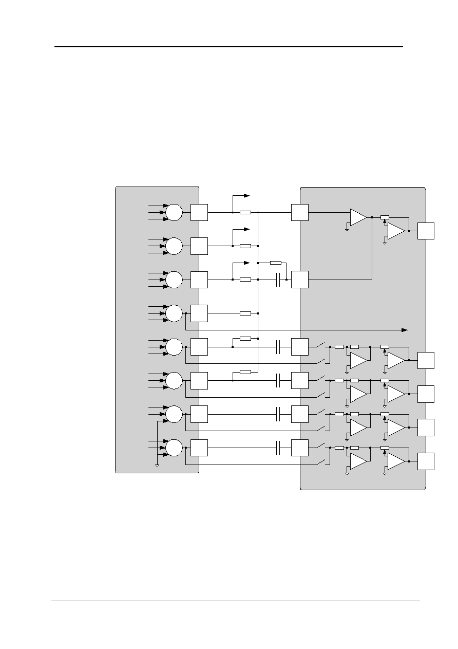
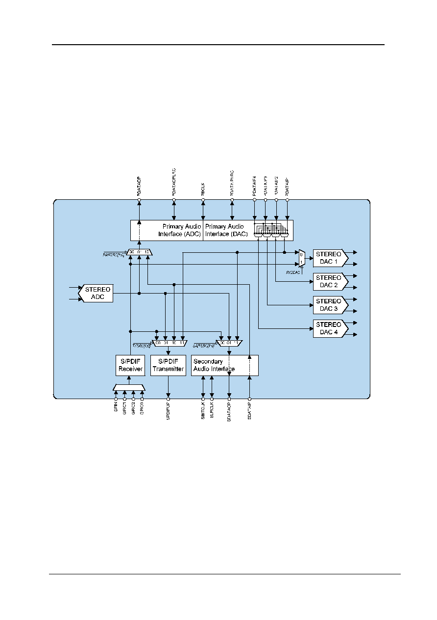
DIGITAL AUDIO INTERFACE ROUTING OPTIONS
The WM8777 has extremely flexible digital audio interface routing options which are illustrated in
Figure 4. It has an S/PDIF receiver, S/PDIF transmitter and two digital audio interfaces. Each DAC
has its own digital input pin PDATAIP1/2/3/4. Internal multiplexors in the primary audio interface
(DAC) allow the data received on any DIN pin to be routed to any DAC .Any DIN pin routed to DAC1
is also routed to the S/PDIF and Secondary Audio Interface transmitters. DAC1 may also be used to
convert received S/PDIF data to analogue, while DACs 2-4 take data only from the primary audio
interface. The primary audio interface can output ADC data, received S/PDIF data or data from the
secondary audio interface on the PDATAOP pin.
The secondary audio interface can output ADC data, received S/PDIF data and data received
through PDATAIP1-4 on the SDATAOP pin. The S/PDIF transmitter can output S/PDIF received
data, and converts ADC data and data from both audio interfaces into S/PDIF format and outputs
them on SPDIFOP.
Figure 4 WM8777 Digital Routing Diagram

Product Preview
WM8777
w
PP Rev 1.94 November 2004
23
REGISTER
ADDRESS
BIT LABEL DEFAULT
DESCRIPTION
0
RX2DAC
0
Received S/PDIF PCM data to DAC.
0 = DAC1 takes data from Primary Audio Interface.
1 = DAC1 takes data from S/PDIF receiver.
Note: If DACs 2, 3 and 4 are disabled, DAC1 uses the
subframe rate of the S/PDIF input with respect to any
selected MCLK. PLL clock should be selected to set the
f
s
mode. If DAC 2, 3 or 4 are enabled, the user must
ensure that DACLRC and the S/PDIF subframe are
operating at the same rate; any difference will cause a
sample slip on DAC1.
2:1
TXSRC[1:0]
00
S/PDIF Transmitter Data Source.
00 = S/PDIF received data.
01 = ADC digital output data.
10 = Secondary Audio Interface received data
11 = DAC Audio Interface Received data.
Note: The output rate is determined by the source of the
data to be transmitted. The ADC outputs S/PDIF at a rate
determined by LRCLK.
5:4
PAIFSRC[1:0]
01
Audio Interface output source
00 = S/PDIF received data
01 = ADC digital output data
10 = Secondary Audio Interface received data
11 = Power-down Primary Audio Interface Transmitter
Note: for cases 00 and 10, the user must ensure that the
source rate matches the transmit rate; any difference will
cause samples to be lost. For optimum performance, the
PAIF should be operated in master mode, with the master
clock source the same as the PAIF source.
R65 (41h)
Interface
Source
Select
7:6
SAIFSRC[1:0]
00
Secondary Audio Interface Transmitter Data Source.
00 = S/PDIF received data.
01 = ADC digital output data.
10 = Power-down Secondary Audio Interface Transmitter
11 = Primary Audio Interface received data.
Note: for cases 00 and 10, the user must ensure that the
source rate matches the transmit rate; any difference will
cause samples to be lost. For case 01, if PAIFSRC is not
also 01, the ADC operation rate is set by the SLRC and
ADCCLKSRC/PLL2ADC register bits.
Table 10 Interface Output Selection Register
WM8777
Product Preview
w
PP Rev 1.94 November 2004
24
CONTROL INTERFACE OPERATION
The WM8777 is controlled using a 2-wire (plus readback pin) or 3-wire (plus readback pin) SPI
compatible serial interface.
The interface configuration is determined by the state of the GPIO/MODE pin on power up. If the
GPIO/MODE pin is low while the power on reset is being applied internally, the 2-wire configuration is
selected. If GPIO/MODE is high while the power on reset is being applied internally, the 3-wire
configuration is selected - see table 11.
The control interface is 5V tolerant, meaning that the control interface input signals CSB, SCLK and
SDIN may have an input high level of 5V while DVDD is 3V. Input thresholds are determined by
DVDD.
GPIO/MODE AT
POWER UP
CONTROL
Low 2-wire
High
3-wire
Table 11 Control Interface Selection
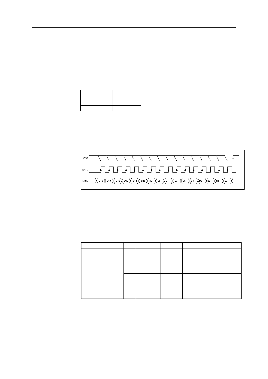
3-WIRE (SPI COMPATIBLE) SERIAL CONTROL MODE WITH ADDITIONAL
READBACK PIN
SDIN is used for the program data, SCLK is used to clock in the program data and CSB is used to
latch the program data. SDIN is sampled on the rising edge of SCLK. The 2-wire interface protocol
with readback is shown in Figure 5.
Figure 5 3 Wire SPI Compatible Interface
1.
B[15:9] are Control Address Bits
2.
B[8:0] are Control Data Bits
3.
CSB is edge sensitive ≠ the data is latched on the rising edge of CSB.
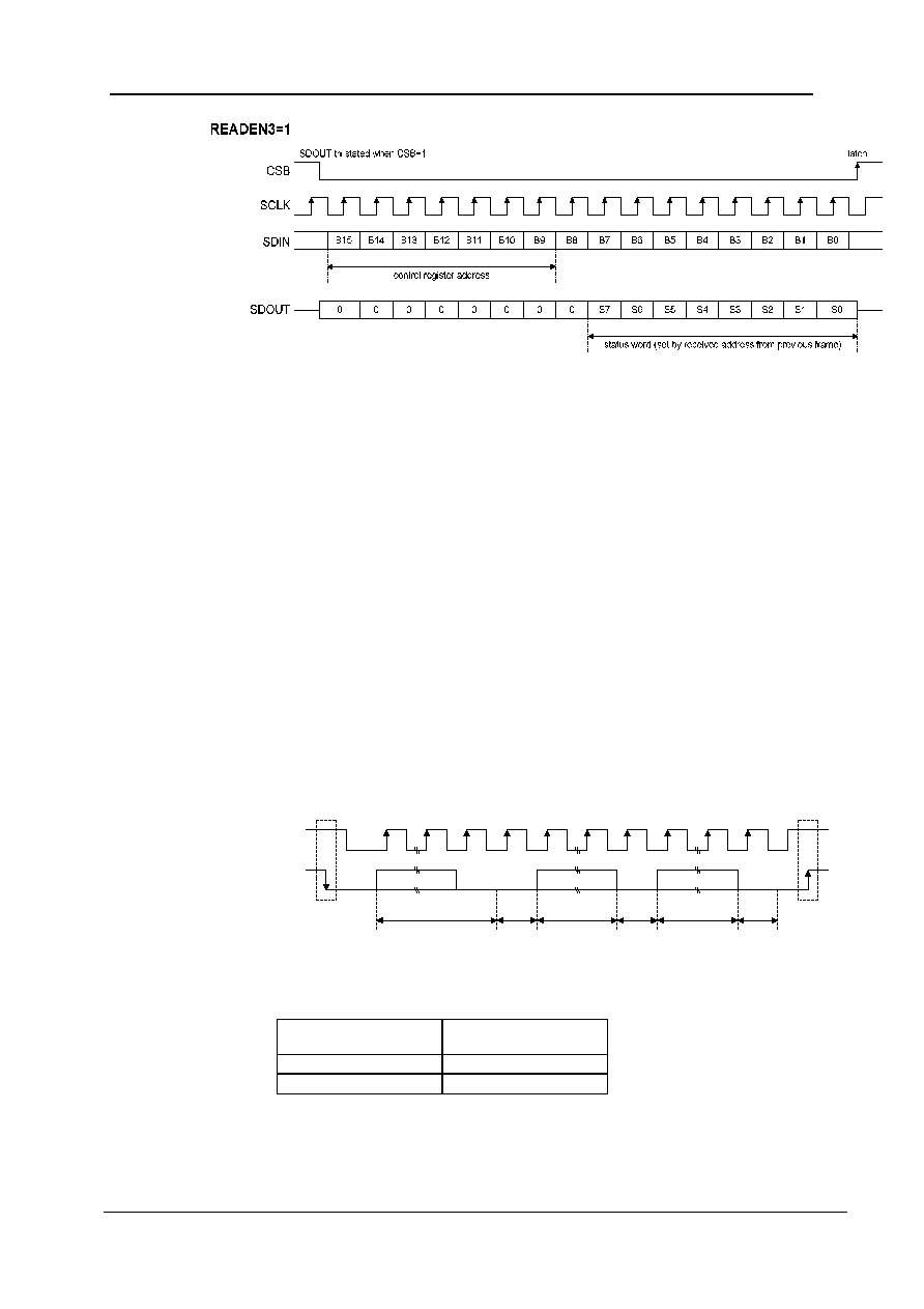
3-WIRE REGISTER READBACK
The read-only registers in the S/PDIF section can be read back via the SDOUT pin. To enable
readback the READEN3 bit must be set.
REGISTER ADDRESS
BIT
LABEL
DEFAULT
DESCRIPTION
4 READEN3
0
3-Wire Read-back mode enable.
0 = 3-Wire read-back mode
disabled
1 = 3-Wire read-back mode
enabled
(4Ah)
Read-back Control
5 READEN2
0
2-Wire Read-back mode enable.
0 = 2-Wire read-back mode
disabled
1 = 2-Wire read-back mode
enabled
Table 12 Readback Control Register
The 3-wire interface readback protocol is shown in Figure 6. Note that the SDOUT pin is tri-state
unless CSB is held low, therefore CSB must be held low for the duration of the read.
Product Preview
WM8777
w
PP Rev 1.94 November 2004
25
Figure 6 3-Wire SPI Compatible Control Interface Readback
2-WIRE SERIAL CONTROL MODE WITH ADDITIONAL READBACK PIN
The WM8777 supports software control via a 2-wire (plus readback pin) serial bus. Many devices can
be controlled by the same bus, and each device has a unique 7-bit address (this is not the same as
the 7-bit address of each register in the WM8777).
The controller indicates the start of data transfer with a high to low transition on SDIN while SCLK
remains high. This indicates that a device address and data will follow. All devices on the 2-wire bus
respond to the start condition and shift in the next eight bits on SDIN (7-bit address + Read/Write bit,
MSB first). If the device address received matches the address of the WM8777, the WM8777
responds by pulling SDIN low on the next clock pulse (ACK). If the address is not recognised, the
WM8777 returns to the idle condition and wait for a new start condition and valid address.
Once the WM8777 has acknowledged a correct address, the controller sends the first byte of control
data (B15 to B8, i.e. the WM8777 register address plus the first bit of register data). The WM8777
then acknowledges the first data byte by pulling SDIN low for one clock pulse. The controller then
sends the second byte of control data (B7 to B0, i.e. the remaining 8 bits of register data), and the
WM8777 acknowledges again by pulling SDIN low.
The transfer of data is complete when there is a low to high transition on SDIN while SCLK is high.
After receiving a complete address and data sequence the WM8777 returns to the idle state and
waits for another start condition. If a start or stop condition is detected out of sequence at any point
during data transfer (i.e. SDIN changes while SCLK is high), the device jumps to the idle condition.
Figure 7 2-Wire Serial Control Interface
The WM8777 has two possible device addresses, which can be selected using the CSBpin.
CSBSTATE
DEVICE ADDRESS IN 2-
WIRE MODE
Low or Unconnected
0011010
High 0011011
Table 13 2-Wire MPU Interface Address Selection
SDIN
SCLK
address
wr
ack
B15-B8
ack
B7-B0
ack
device address
[wr=0]
in
STOP
START
out
out
out
in
in
register
address and
1st data bit
remaining data
bits

WM8777
Product Preview
w
PP Rev 1.94 November 2004
26
2-WIRE SERIAL READBACK
The WM8777 allows readback of certain registers in 2-wire mode, with data output on the SDOUT
pin. Readback is set by writing to the Readback Control register (see Table 12) to set READEN2 to
1.
Figure 8 2-Wire Readback
Product Preview
WM8777
w
PP Rev 1.94 November 2004
27
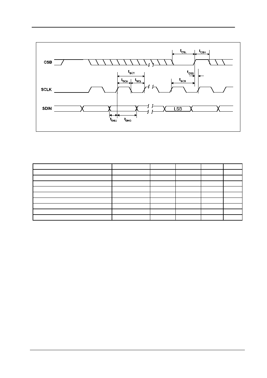
CONTROL INTERFACE TIMING ≠ 3-WIRE MODE
Figure 9 SPI Compatible Control Interface Input Timing
Test Conditions
DVDD = 3.3V, AGND = 0V, DGND = 0V, T
A
= +25
o
C, fs = 48kHz, MCLK = 256fs, ADC/DAC in Slave Mode unless otherwise
stated.
PARAMETER SYMBOL
MIN
TYP
MAX
UNIT
SCLK rising edge to CSBrising edge
t
SCS
60
ns
SCLK pulse cycle time
t
SCY
80
ns
SCLK pulse width low
t
SCL
30
ns
SCLK pulse width high
t
SCH
30
ns
SDIN to SCLK set-up time
t
DSU
20
ns
SCLK to SDIN hold time
t
DHO
20
ns
CSB pulse width low
t
CSL
20
ns
CSB pulse width high
t
CSH
20
ns
CSB rising to SCLK rising
t
CSS
20
ns
Table 14 SCLK Timing Requirements

WM8777
Product Preview
w
PP Rev 1.94 November 2004
28
CONTROL INTERFACE TIMING ≠ 2-WIRE MODE
Figure 10 Control Interface Timing ≠ 2-Wire Serial Control Mode (MODE=0)
Test Conditions
AVDD = 5V, DVDD = 3.3V, AGND, DGND = 0V, T
A
= +25
o
C, fs = 48kHz, MCLK = 256fs unless otherwise stated
PARAMETER SYMBOL
MIN
TYP
MAX
UNIT
Program Register Input Information
SCLK Frequency
0
400
kHz
SCLK Low Pulse-Width
t
1
600
ns
SCLK High Pulse-Width
t
2
1.3
us
Hold Time (Start Condition)
t
3
600
ns
Setup Time (Start Condition)
t
4
600
ns
Data Setup Time
t
5
100
ns
SDIN, SCLK Rise Time
t
6
300
ns
SDIN, SCLK Fall Time
t
7
300
ns
Setup Time (Stop Condition)
t
8
600
ns
Data Hold Time
t
9
900
ns
Pulse width of spikes that will be suppressed
t
ps
0
5
ns
Table 15 2-wire Control Interface Timing Information.
t
3
t
1
t
6
t
9
t
2
t
5
t
7
t
3
t
4
t
8
SDIN
SCLK

Product Preview
WM8777
w
PP Rev 1.94 November 2004
29
MASTER CLOCK
In a typical digital audio system there is only one central clock source producing a reference clock to
which all audio data processing is synchronised. This clock is often referred to as the audio system's
Master Clock. The external master system clock can be applied directly through the MCLK input pin
with no software configuration necessary. In a system where there are a number of possible sources
for the reference clock it is recommended that the clock source with the lowest jitter be used to
optimise the performance of the ADC and DAC.
MASTER CLOCK TIMING
Figure 11 Master Clock Timing Requirements
Test Conditions
DVDD = 3.3V, DGND = 0V, T
A
= +25
o
C, fs = 48kHz, MCLK = 256fs, ADC/DAC in Slave Mode unless otherwise stated.
PARAMETER SYMBOL
TEST
CONDITIONS
MIN
TYP
MAX
UNIT
System Clock Timing Information
MCLK System clock pulse width high
t
MCLKH
11
ns
MCLK System clock pulse width low
t
MCLKL
11
ns
MCLK System clock cycle time
t
MCLKP
28
ns
MCLK Duty cycle
40:60
60:40
Table 16 Master Clock Timing Requirements
The master clock for WM8777 supports DAC and ADC audio sampling rates from 128fs to 1152fs,
where fs is the audio sampling frequency (PDATAIPLRC or PDATAOPLRC) typically 32kHz,
44.1kHz, 48kHz, 96kHz, or 192KHz. The master clock is used to operate the digital filters and the
noise shaping circuits.
The WM8777 has a master clock detection circuit that automatically determines the relationship
between the master clock frequency and the sampling rate (to within +/- 32 system clocks). If there is
a greater than 32 clocks error the interface sets itself to the highest rate available, 1152fs. The
master clock must be synchronised with PDATAOPLRC/PDATAIPLRC, although the WM8777 is
tolerant of phase variations or jitter on this clock.
t
MCLKL
t
MCLKH
t
MCLKP
MCLK
WM8777
Product Preview
w
PP Rev 1.94 November 2004
30
AUDIO SAMPLING RATES AND AUDIO INTERFACES
DIGITAL AUDIO INTERFACES
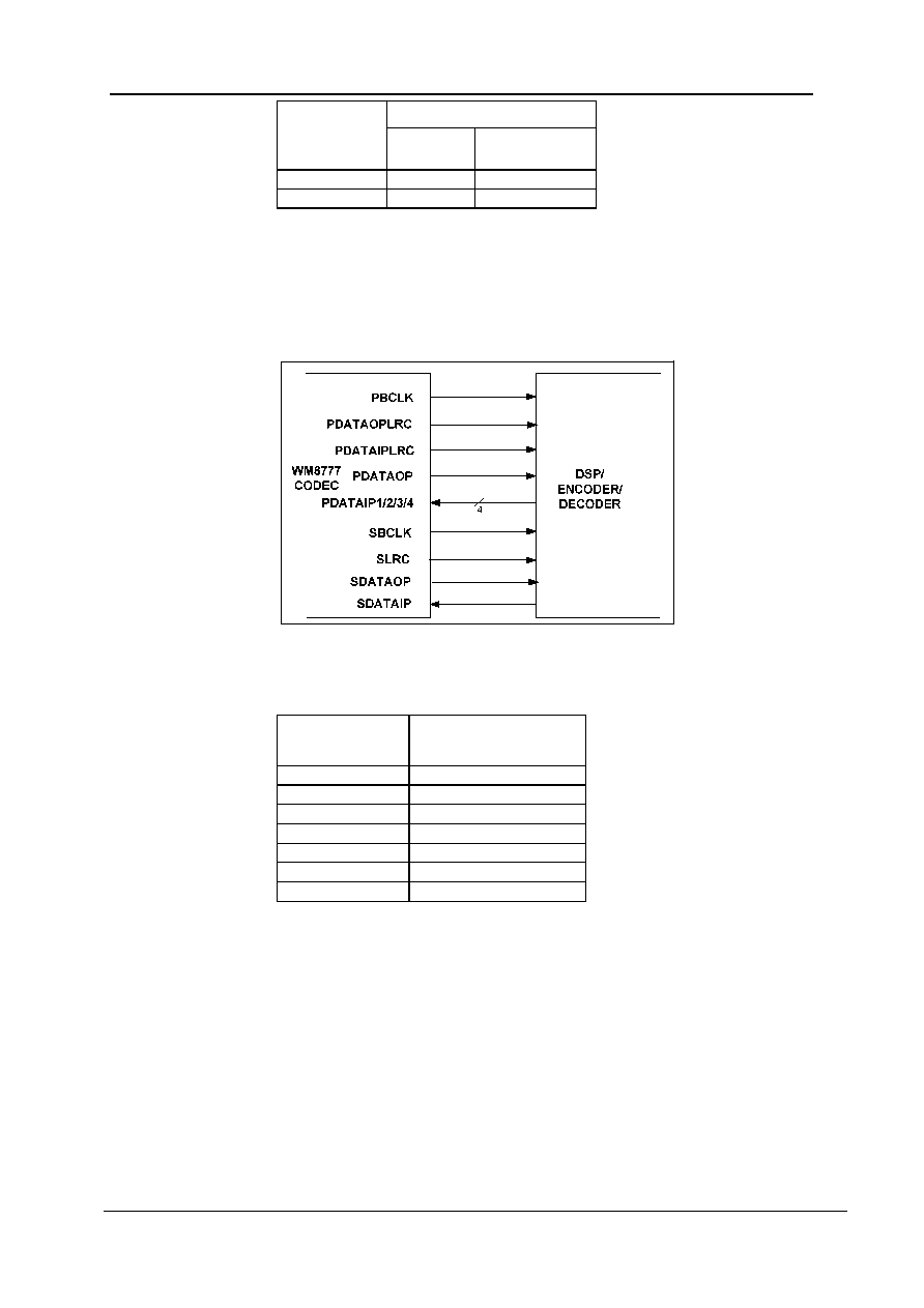
The WM8777 has two audio interfaces ≠ a primary audio interface and a secondary audio interface.
The primary audio interface has four data inputs (PDATAIP1/2/3/4), one data output (PDATAOP),
and is controlled by PBCLK, PDATAOPLRC and PDATAIPLRC clock pins. The secondary audio
interface has one input (SDATAIP), one output (SDATAOP) and is controlled by SPBCLK and SLRC
clock pins.
Both audio interfaces operate in either Slave or Master mode, selectable using the PAIFRX_MS and
SMS control bits. In both Master and Slave modes PDATAIP1/2/3/4 and SDATAIP are always inputs
to the WM8777 and PDATAOP and SDATAOP are always outputs. The default is Slave mode.
SLAVE MODE
In Slave mode (PAIFRX_MS/SMS=0) PDATAOPLRC, PDATAIPLRC, SLRC, PBCLK and SPBCLK
are inputs to the WM8777. PDATAIP1/2/3/4, PDATAOPLRC and PDATAIPLRC are sampled by the
WM8777 on the rising edge of PBCLK. SDATAIP and SLRC are sampled by the WM8777 on the
rising edge of SBCLK. Data output PDATAOP changes on the falling edge of PBCLK and data output
on SDATAOP changes on the falling edge of SBCLK. By setting control bit PAIFRX_BCP the polarity
of PBCLK may be reversed so that PDATAIP1/2/3/4, PDATAOPLRC and PDATAIPLRC are sampled
on the falling edge of PBCLK and PDATAOP changes on the rising edge of PBCLK. Similarly the
polarity of SBCLK can be reversed using control bit SBCP.
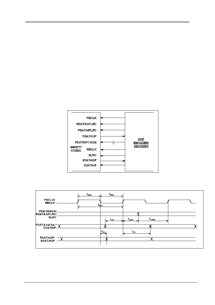
Figure 12 Digital Audio Interface ≠ Slave Mode
Figure 13 Digital Audio Data Timing ≠ Slave Mode

Product Preview
WM8777
w
PP Rev 1.94 November 2004
31
Test Conditions
DVDD = 3.3V, DGND = 0V, T
A
= +25
o
C, fs = 48kHz, MCLK = 256fs, ADC/DAC in Slave Mode unless otherwise stated.
PARAMETER SYMBOL
TEST
CONDITIONS
MIN
TYP
MAX
UNIT
Audio Data Input Timing Information
PBCLK cycle time
t
BCY
50
ns
PBCLK pulse width high
t
BCH
20
ns
PBCLK pulse width low
t
BCL
20
ns
PDATAIPLRC/PDATAOPL
RC set-up time to PBCLK
rising edge
t
LRSU
10
ns
PDATAIPLRC/PDATAOPL
RC hold time from PBCLK
rising edge
t
LRH
10
ns
PDATAIP1/2/3/4 set-up
time to PBCLK rising edge
t
DS
10
ns
PDATAIP1/2/3/4 hold time
from PBCLK rising edge
t
DH
10
ns
PDATAOP propagation
delay from PBCLK falling
edge
t
DD
0
10
ns
Table 17 Digital Audio Data Timing ≠ Slave Mode
Note: PDATAOPLRC and PDATAIPLRC should be synchronous with MCLK, although the WM8777 interface is tolerant of
phase variations or jitter on these signals.
The DACs support system clock to sampling clock ratios of 256fs to 1152fs when the DAC signal
processing of the WM8777 is programmed to operate at 128 times oversampling rate (DACOSR=0).
The DACs support ratios of 128fs and 192fs when the WM8777 is programmed to operate at 64
times oversampling rate (DACOSR=1).
The ADC supports system clock to sampling clock ratios of 128fs to 1152fs. The signal processing
for the WM8777 ADC typically operates at an oversampling rate of 128fs. For ADC operation at
96kHz in 256fs or 384fs mode it is recommended that the user set the ADCOSR bit. This changes
the ADC signal processing oversample rate from 128fs to 64fs. For ADC operation at 192kHz in
128fs or 192fs mode it is recommended that the user set the ADCOSR bit. This changes the ADC
signal processing oversample rate from 64fs to 32fs.
Table 18 shows the typical system clock frequencies for ADC operation at both 128 times
oversampling rate (ADCOSR=0) and 64 times oversampling rate (ADCOSR=1), and DAC operation
at 128 times oversampling rate (DACOSR=0). Table 19 shows typical system clock frequencies for
ADC operation at 32/64 times oversampling rate (ADCOSR=1), and DAC operation at 64 times
oversampling rate (DACOSR =1).
System Clock Frequency (MHz)
SAMPLING
RATE
(PDATAIPLRC/
PDATAOPLRC)
256fs 384fs 512fs 768fs 1152fs
32kHz 8.192
12.288 16.384 24.576 36.864
44.1kHz 11.2896
16.9340 22.5792 33.8688
Unavailable
48kHz 12.288
18.432
24.576
36.864
Unavailable
96kHz
24.576
36.864
Unavailable Unavailable Unavailable
Table 18 ADC and DAC system clock frequencies versus sampling rate. (ADC operation at
either 128 times oversampling rate (ADCOSR=0) or 64 times oversampling rate (ADCOSR=1),
DAC operation at 128 times oversampling rate, DACOSR=0)
WM8777
Product Preview
w
PP Rev 1.94 November 2004
32
System Clock Frequency (MHz)
SAMPLING
RATE
(PDATAIPLRC/
PDATAOPLRC)
128fs 192fs
96kHz 12.288 18.432
192kHz 24.576 36.864
Table 19 ADC and DAC system clock frequencies versus sampling rate. (ADC operation at
32/64 times oversampling rate (ADCOSR=1), DAC operation at 64 times oversampling rate
(DACOSR=1)
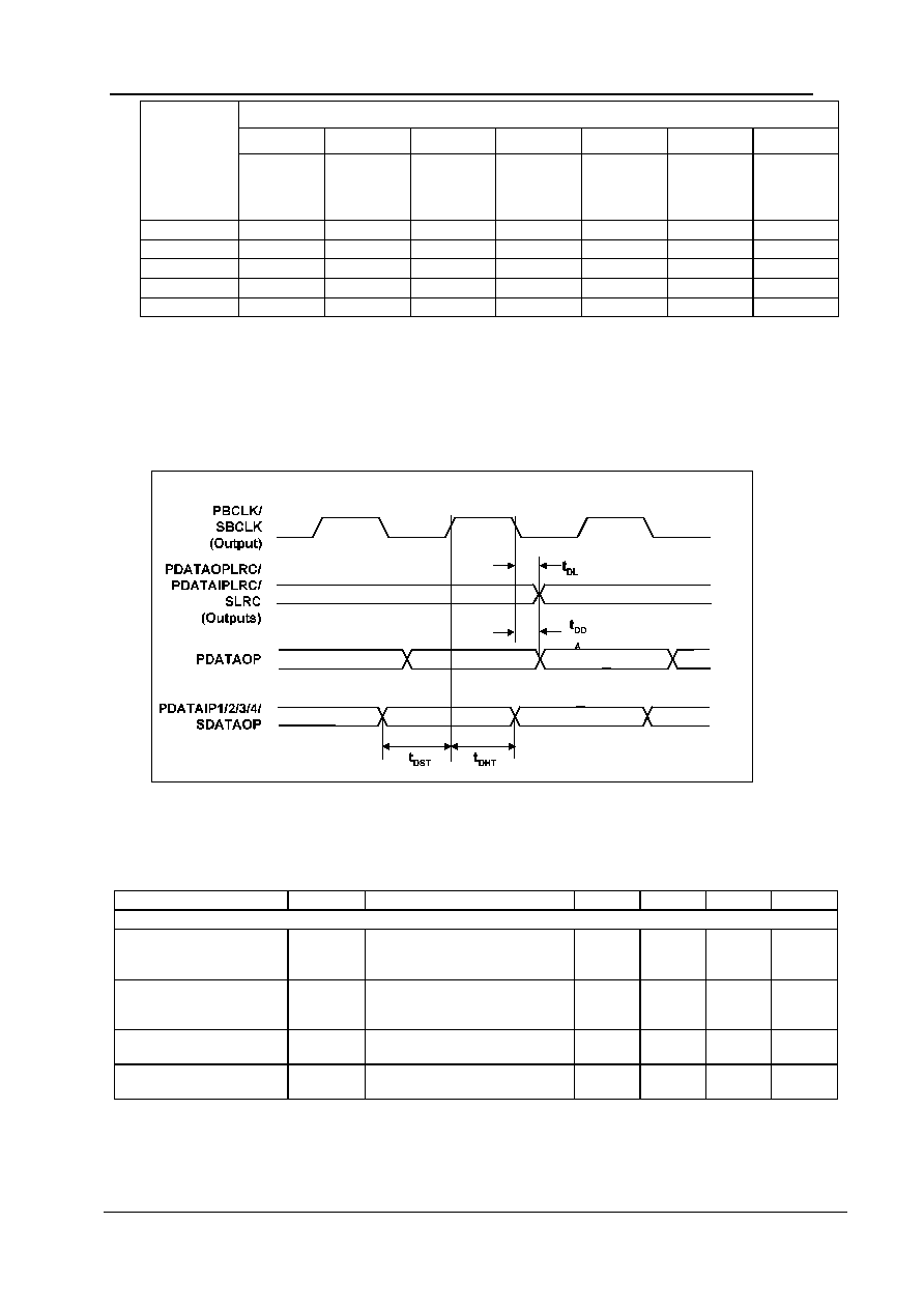
MASTER MODE
In Master mode PBCLK, PDATAIPLRC, PDATAOPLRC, SLRC and SPBCLK are generated by the
WM8777.
Figure 14 Audio Interface - Master Mode
The frequencies of PDATAOPLRC, PDATAIPLRC and SLRC are set by setting the required ratio of
MCLK to PDATAIPLRC, PDATAOPLRC and SLRC using the PAIFRX_RATE, PAIFTX_RATE and
SAIFRATE control bits respectively, see Table 20.
PAIFTX_RATE[2:0]/
PAIFRX_RATE[2:0]
MCLK :
PDATAOPLRC/PDATAIPLR
C/SLRC RATIO
000 128fs
001 192fs
010 256fs
011 384fs
100 512fs
101 768fs
110 1152fs
Table 20 Master Mode MCLK:LRCLK Ratio Select
Table 21 shows the settings for PAIFTX_RATE, PAIFRX_RATE and SAIFRATE for common sample
rates and MCLK frequencies.
Product Preview
WM8777
w
PP Rev 1.94 November 2004
33
SYSTEM CLOCK FREQUENCY (MHZ)
128fs 192fs 256fs 384fs 512fs 768fs 1152fs
SAMPLING
RATE
(PDATAIPLRC/
PDATAOPLRC)
PAIFTX_RATE/
PAIFRX_RATE/
SAIFRATE
=000
PAIFTX_RATE/
PAIFRX_RATE/
SAIFRATE
=001
PAIFTX_RATE/
PAIFRX_RATE/
SAIFRATE
=010
PAIFTX_RATE/
PAIFRX_RATE/
SAIFRATE
=011
PAIFTX_RATE/
PAIFRX_RATE/
SAIFRATE
=100
PAIFTX_RATE/
PAIFRX_RATE/
SAIFRATE
=101
PAIFTX_RATE/
PAIFRX_RATE/
SAIFRATE
=110
32kHz 4.096 6.144 8.192 12.288
16.384
24.576
36.864
44.1kHz 5.6448 8.467 11.2896
16.9340
22.5792
33.8688
Unavailable
48kHz 6.144 9.216 12.288 18.432 24.576 36.864
Unavailable
96kHz 12.288 18.432 24.576 36.864
Unavailable
Unavailable
Unavailable
192kHz
24.576
36.864
Unavailable Unavailable Unavailable Unavailable Unavailable
Table 21 Master Mode ADC/PDATAIPLRC Frequency Selection
PBCLK is also generated by the WM8777. The frequency of PBCLK depends on the mode of
operation. In 128/192fs modes (PAIFTX_RATE/PAIFRX_RATE=000 or 001) PBCLK = MCLK/2. In
256/384/512/768/1152fs modes (PAIFTX_RATE/PAIFRX_RATE=010 or 011 or 100 or 101 or 110)
PBCLK = MCLK/4. However if DSP mode is selected as the audio interface mode then
PBCLK=MCLK. This is to ensure that there are sufficient PBCLKs to clock in all eight channels. Note
that DSP mode cannot be used in 128fs mode for word lengths greater than 16-bits or in 192fs mode
for word lengths greater than 24 bits.
Figure 15 Digital Audio Data Timing ≠ Master Mode
Test Conditions
DVDD = 3.3V, DGND = 0V, T
A
= +25
o
C, fs = 48kHz, MCLK = 256fs, ADC/DAC in Slave Mode unless otherwise stated.
PARAMETER SYMBOL
TEST
CONDITIONS
MIN
TYP
MAX
UNIT
Audio Data Input Timing Information
PDATAOPLRC/PDATAIPL
RC propagation delay from
PBCLK falling edge
t
DL
0
10
ns
PDATAOP propagation
delay from PBCLK falling
edge
t
DDA
0
10
ns
PDATAIP1/2/3/4 setup time
to PBCLK rising edge
t
DST
10
ns
PDATAIP1/2/3/4 hold time
from PBCLK rising edge
t
DHT
10
ns
Table 22 Digital Audio Data Timing ≠ Master Mode

WM8777
Product Preview
w
PP Rev 1.94 November 2004
34
MASTER MODE REGISTERS
Control bit PAIFRX_MS selects between primary audio interface Master and Slave Modes. Control bit
SMS selects between secondary audio interface master and slave modes.
REGISTER
ADDRESS
BIT LABEL DEFAULT
DESCRIPTION
7
PAIFTX_MS
0
Master/Slave Interface mode select. If
ADCCLKSRC is set high then this register
control whether the ADC clocks are in
master or slave mode/
0 = Slave Mode ≠ PDATAOPLRC and
ADCPBCLK are inputs
1 = Master Mode ≠ PDATAOPLRC and
ADCPBCLK are outputs
(19h)
Master Mode
Control
8
PAIFRX_MS
0
Maser/Slave interface mode select
0 = Slave Mode ≠ PDATAOPLRC,
PDATAIPLRC and PBCLK are inputs
1 = Master Mode ≠ PDATAOPLRC,
PDATAIPLRC and PBCLK are outputs
Note if ADCCLKSRC is set high then this
register only controls PDATAIPLRC and
PBCLK.
(3Fh)
Secondary
Interface
Master Mode
Control
3
SMS
0
Master/Slave interface mode select
0 = Slave Mode ≠ SLRC and SPBCLK are
inputs
1 = Master Mode ≠ SLRC and SPBCLK are
outputs
Table 23 Master Mode Registers
In Master mode the WM8777 generates PDATAOPLRC, PDATAIPLRC and PBCLK. These clocks
are derived from master clock and the ratio of MCLK to PDATAOPLRC and PDATAIPLRC are set by
PAIFTX_RATE, PAIFRX_RATE and SAIFRATE.
REGISTER ADDRESS
BIT
LABEL
DEFAULT
DESCRIPTION
2:0
PAIFTX_RATE
[2:0]
010
(19h)
Master Mode Control
6:4
PAIFRX_RATE
[2:0]
010
(3Fh)
Secondary Interface
Master Mode Control
2:0
SAIFRATE
[2:0]
010
Master Mode MCLK:LRCLK
ratio select:
000 = 128fs
001 = 192fs
010 = 256fs
011 = 384fs
100 = 512fs
101 = 768fs
110 = 1152fs
(3Fh)
Secondary Interface
5:4 SAIFCLKSRC[1:0] 00
Audio interface master clock
source when SMS is 1.
00 = MCLK
01 = GPIO (If ADCCLKSRC
is set)
10 = PLL clock
11 = PLL clock
Table 24 Master Mode MCLK:LRCLK Regsiters
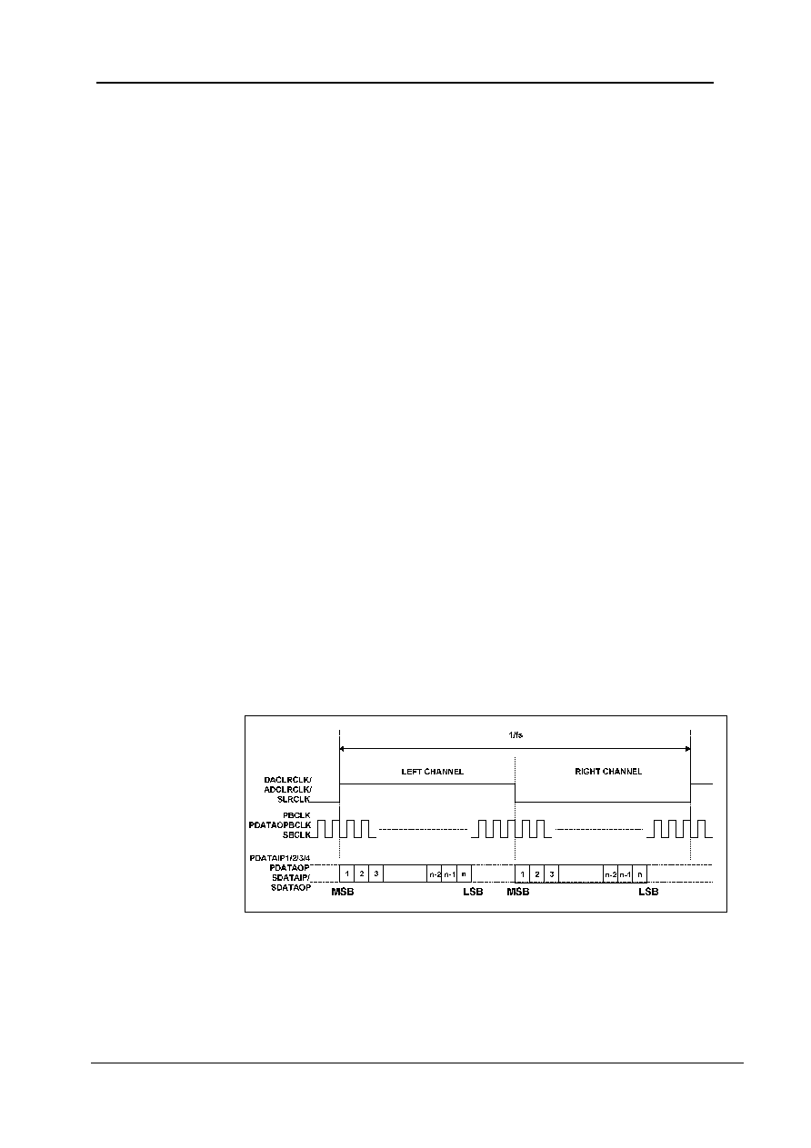
Product Preview
WM8777
w
PP Rev 1.94 November 2004
35
AUDIO INTERFACE FORMATS
Audio data is applied to the WM8777 via the Primary and Secondary Audio Interface. Five popular
interface formats are supported:
∑
Left Justified mode
∑
Right Justified mode
∑
I
2
S mode
∑
DSP Early mode
∑
DSP Late mode
All five formats send the MSB first and support word lengths of 16, 20, 24 and 32 bits, with the
exception of 32 bit right justified mode, which is not supported.
Audio Data for each stereo channel is time multiplexed with the interface's Left-Right-Clock
(PDATAOPLRC/PDATAIPLRC), indicating whether the left or right channel is present. The
PDATAOPLRC/PDATAIPLRC is also used as a timing reference to indicate the beginning or end of
the data words.
In left justified, right justified and I
≤
S modes, the minimum number of PBCLKs per LRCLK period is 2
times the selected word length. LRCLK must be high for a minimum of word length PBCLKs and low
for a minimum of word length PBCLKs. Any mark to space ratio on LRCLK is acceptable provided
the above requirements are met. The Primary Audio interface has Left-Right-Clocks PDATAOPLRC
and PDATAIPLRC, and Bit-Clock PBCLK. The Secondary Audio Interface has Left-Right-Clock
SLRC, and Bit-Clock SPBCLK.
In DSP early or DSP late mode, all 8 DAC channels are time multiplexed onto PDATAIP1.
PDATAIPLRC is used as a frame sync signal to identify the MSB of the first word. The minimum
number of PBCLKs per PDATAIPLRC period is 8 times the selected word length. Any mark to space
ratio is acceptable on PDATAIPLRC provided the rising edge is correctly positioned. The ADC data
may also be output in DSP early or late modes, with PDATAOPLRC used as a frame sync to identify
the MSB of the first word. The minimum number of PBCLKs per PDATAOPLRC period is 2 times the
selected word length. The Secondary Audio Interface also supports DSP modes with SLRC used as
a frame sync and data input on SDATAIP, and data output on SDATAOP. The minimum number of
SPBCLKs per SLRC period is 2 times the selected word length.
LEFT JUSTIFIED MODE
In left justified mode, the MSB of the input data (PDATAIP/SDATAIP) is sampled by the WM8777 on
the first rising edge of PBCLK/SPBCLK following a LRCLK transition. The MSB of the output data
(PDATAOP/SDATAOP) changes on the same falling edge of PBCLK as SLRC, and may be sampled
on the next rising edge of PBCLK. LRCLKs are high during the left samples and low during the right
samples.
Figure 16 Left Justified Mode Timing Diagram
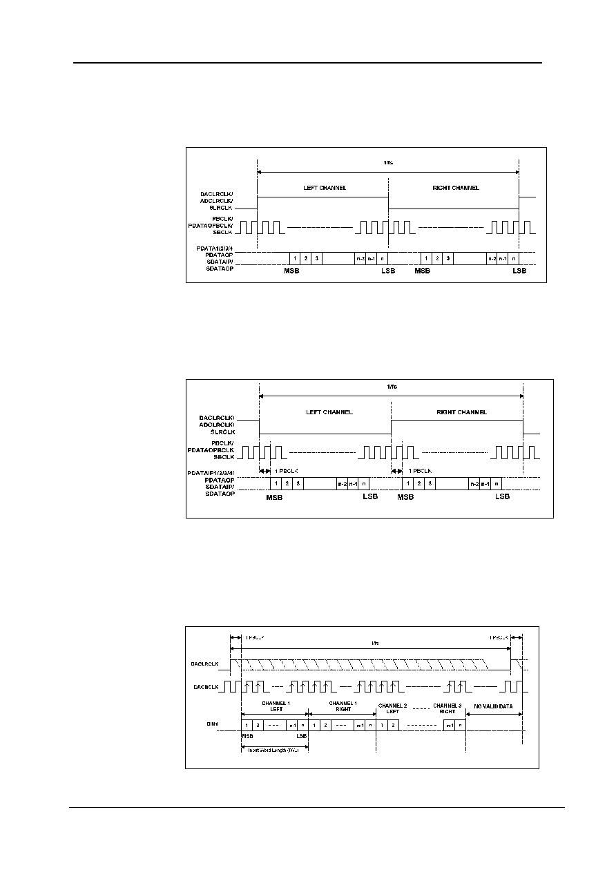
WM8777
Product Preview
w
PP Rev 1.94 November 2004
36
RIGHT JUSTIFIED MODE
In right justified mode, the LSB of the input data (PDATAIP/SDATAIP) is sampled by the WM8777 on
the rising edge of PBCLK/SPBCLK preceding a LRCLK transition. The LSB of the output data
(PDATAOP/SDATOP) changes on the falling edge of PBCLK preceding a LRCLK transition, and may
be sampled on the nect rising edge of PBCLK. LRCLKs are high during the left samples and low
during the right samples (Figure 17).
Figure 17 Right Justified Mode Timing Diagram
I
2
S MODE
In I
2
S mode, the MSB of the input data is sampled by the WM8777 on the second rising edge of
PBCLK/SPBCLK following a LRCLK transition. The MSB of the output data changes on the first
falling edge of PBCLK following an LRCLK transition, and may be sampled on the next rising edge of
PBCLK. LRCKs are low during the left samples and high during the right samples.
Figure 18 I
2
S Mode Timing Diagram
DSP EARLY MODE
In DSP early mode, the MSB of DAC channel 1 left data is sampled by the WM8777 on the second
rising edge on PBCLK following a PDATAIPLRC rising edge. DAC channel 1 right and DAC channels
2, 3 and 4 data follow DAC channel 1 left data (Figure 19).
Figure 19 DSP Early Mode Timing Diagram ≠ DAC Data Input

Product Preview
WM8777
w
PP Rev 1.94 November 2004
37
The MSB of the left channel ADC data is output on PDATAOP and changes on the first falling edge
of PBCLK following a low to high PDATAOPLRC transition and may be sampled on the rising edge of
PBCLK. The right channel ADC data is contiguous with the left channel data (Figure 20).
Figure 20 DSP Early Mode Timing Diagram ≠ ADC Data Output
DSP LATE MODE
In DSP late mode, the MSB of DAC channel 1 left data is sampled by the WM8777 on the first
PBCLK rising edge following a PDATAIPLRC rising edge. DAC channel 1 right and DAC channels 2,
3 and 4 data follow DAC channel 1 left data (Figure 21).
Figure 21 DSP Late Mode Timing Diagram ≠ DAC Data Input
The MSB of the left channel ADC data is output on PDATAOP and changes on the same falling edge
of PBCLK as the low to high PDATAOPLRC transition and may be sampled on the rising edge of
PBCLK. The right channel ADC data is contiguous with the left channel data (Figure 22).
Figure 22 DSP Late Mode Timing Diagram ≠ ADC Data Output
In both early and late DSP modes, DACL1 is always sent first, followed immediately by DACR1 and
the data words for the other 6 channels. No PBCLK edges are allowed between the data words. The
word order is DAC1 left, DAC1 right, DAC2 left, DAC2 right, DAC3 left, DAC3 right, DAC4 left, DAC4
right. For DSP modes the Secondary Audio Interface exhibits similar timing to the ADC where data is
input on SDATAIP, and output on SDATAOP.

WM8777
Product Preview
w
PP Rev 1.94 November 2004
38
DIGITAL AUDIO INTERFACE CONTROL REGISTERS
Interface format for primary and secondary interfaces are selected via the PAIFRX_FMT register bits:
REGISTER ADDRESS
BIT
LABEL
DEFAULT
DESCRIPTION
(18h)
Primary
Interface Control (RX)
1:0 PAIFRX_FMT
[1:0]
10
(1Bh)
Primary Interface
Control (TX)
1:0 PAIFTX_FMT
[1:0]
10
(3Eh)
Secondary Interface
Control
1:0 SAIF_FMT
[1:0]
10
Interface Format Select
00 = right justified mode
01 = left justified mode
10 = I
2
S mode
11 = DSP (early or late)
mode
Table 25 Format Registers
In left justified, right justified or I
2
S modes, the PAIFRX_LRP register bit controls the polarity of
PDATAIPLRC/PDATAOPLRC/SLRC. If this bit is set high, the expected polarity of
PDATAIPLRC/PDATAOPLRC/SLRC will be the opposite of that shown in Figure 16, Figure 17 and
Figure 18.
Note that if this feature is used as a means of swapping the left and right channels, a 1 sample
phase difference will be introduced. In DSP modes, the PAIFRX_LRP register bit is used to select
between early and late modes.
REGISTER ADDRESS
BIT
LABEL
DEFAULT
DESCRIPTION
(18h)
Primary
Interface Control (RX)
2 PAIFRX_LRP
0
(1Bh)
Primary Interface
Control (TX)
2 PAIFTX_LRP
0
(3Eh)
Secondary Interface
Control
2 SAIF_LRP
0
In LEFT/RIGHT/I
2
S modes:
PDATAOPLRC/PDATAIPLRC/SLRC
Polarity (normal)
0 = normal LRCLK polarity
1 = inverted LRCLK polarity
In DSP mode:
0 = Early DSP mode
1 = Late DSP mode
Table 26 LRCLK Polarity Registers
By default, PDATAIPLRC, PDATAOPLRC, SLRC, PDATAIP1/2/3/4 and SDATAIP are sampled on
the rising edge of PBCLK/SPBCLK and should ideally change on the falling edge. Data sources that
change PDATAIPLRC, PDATAOPLRC, SLRC, PDATAIP1/2/3/4 and SDATAOP on the rising edge of
PBCLK/SPBCLK can be supported by setting the PAIFRX_BCP register bit. Setting PAIFRX_BCP to
1 inverts the polarity of PBCLK/SPBCLK to the inverse of that shown in Figure 19, Figure 20, Figure
21 and Figure 22.
REGISTER ADDRESS
BIT
LABEL
DEFAULT
DESCRIPTION
(18h)
Primary
Interface Control (RX)
3 PAIFRX_BCP
0
(1Bh)
Primary Interface
Control (TX)
3 PAIFTX_BCP
0
(3Eh)
Secondary Interface
Control
3 SAIF_BCP
0
PBCLK/SPBCLK Polarity (DSP
modes)
0 = normal PBCLK polarity
1 = inverted PBCLK polarity
Table 27 PBCLK Polarity Registers
The PAIFRX_WL[1:0] bits are used to control the input word length.
Note: If 32-bit mode is selected in right justified mode, the WM8777 defaults to 24 bits.

Product Preview
WM8777
w
PP Rev 1.94 November 2004
39
REGISTER ADDRESS
BIT
LABEL
DEFAULT
DESCRIPTION
(18h)
Primary
Interface Control (RX)
5:4 PAIFRX_WL[1:0]
10
(1Bh)
Primary Interface
Control (TX)
5:4 PAIFTX_WL
[1:0]
10
(3Eh)
Secondary Interface
Control
5:4 SAIF_WL
[1:0]
10
Input Word Length
00 = 16 bit data
01 = 20 bit data
10 = 24 bit data
11 = 32 bit data
Table 28 Word Length Registers
In all modes, the data is signed 2's complement. The digital filters always input 24-bit data. If the
DAC is programmed to receive 16 or 20 bit data, the WM8777 pads the unused LSBs with zeros. If
the DAC is programmed into 32 bit mode, the 8 LSBs are ignored.
Note: In 24 bit I
≤
S mode, any width of 24 bits or less is supported provided that LRCLK is high for a
minimum of 24 PBCLKs and low for a minimum of 24 PBCLKs. If exactly 32 bit clocks occur in one
left/right clock (16 high, 16 low) the chip will auto detect and run a 16 bit data mode.
POWERDOWN MODES
The WM8777 has powerdown control bits allowing specific parts of the WM8777 to be powered down
when not in use. The 6-channel input source selector and input buffer may be powered down using
control bit AINPD. When AINPD is set all inputs to the source selector (AIN1L/R to AIN6L/R) are
switched to a buffered VMIDADC and the ADC is also powered off. The control bit ADCPO powers
off the ADC.
The four stereo DACs each have a separate powerdown control bit, DACPD[3:0] allowing individual
stereo DACs to be powered down when not in use. The analogue output mixers and PGAs may also
be powered down by setting OUTPD1/2/3/4. OUTPD1/2/3/4 also switch the analogue outputs
VOUTL/R to VMIDDAC to maintain a dc level on the output. SPDIFTXD and SPDIFRXD will
powerdown the S/PDIF transmitter and receiver.
Setting all of AINPD, ADCPD, DACPD[3:0], SPDIFTXD, SPDIFRXD and OUTPD[3:0] will powerdown
everything except the references VMIDADC, ADCREF and VMIDDAC. These may be powered down
by setting PDWN. Setting PDWN will override all other powerdown control bits. It is recommended
that the 6-channel input mux and buffer, ADC, DAC and output mixers and PGAs are powered down
before setting PDWN. The default is for all powerdown bits to be set except PDWN.
REGISTER ADDRESS
BIT
LABEL
DEFAULT
DESCRIPTION
0
PWDN
0
Chip Powerdown Control (works
in tandem with the other
powerdown registers):
0 = All digital circuits running,
outputs are active
1 = All digital circuits in power
save mode, outputs muted
1 ADCPD
1 ADC powerdown:
0 = ADC enabled
1 = ADC disabled
5:2 DACPD[3:0]
1111
DAC powerdowns (0 = DAC
enabled, 1 = DAC disabled)
DACPD[0] = DAC1
DACPD[1] = DAC2
DACPD[2] = DAC3
DACPD[3] = DAC4
6 SPDIFTXD
1
SPDIF_TX powerdown
0 = SPDIF_TX enabled
1 = SPDIF_TX disabled
(1Ah)
Powerdown Control
7 SPDIFRXD
1
SPDIF_RX powerdown
0 = SPDIF_RX enabled
1 = SPDIF_RX disabled

WM8777
Product Preview
w
PP Rev 1.94 November 2004
40
8
OSCPD
1
OSC power down
0 = Oscillator enabled
1 = Oscillator disabled
(31h)
ADC Mux and Buffer
Powerdown Control
8 AINPD
1 Input mux and buffer powerdown
0 = Input mux and buffer enabled
1 = Input mux and buffer powered
down
7
OUTPD1 1
Mixer Powerdown select
0 = Powerup
1 = Powerdown
(32h)
Output Mux and
Powerdown Control 1
8
OUTPD2 1
Mixer Powerdown select
0 = Powerup
1 = Powerdown
7
OUTPD3 1
Mixer Powerdown select
0 = Powerup
1 = Powerdown
(33h)
Output Mux and
Powerdown Control 2
8
OUTPD4 1
Mixer Powerdown select
0 = Powerup
1 = Powerdown
(37h)
PLL Control 4
0
PLLPD
1
0 = Enable PLL
1 = Disable PLL
0
AUXLPD
1
Auxiliary left output powerdown.
0 = enabled
1 = disabled
1
AUXRPD
1
Auxiliary left output powerdown.
0 = enabled
1 = disabled
2
SURLPD
1
Surround left output powerdown.
0 = enabled
1 = disabled
3
SURRPD
1
Surround Right output
powerdown.
0 = enabled
1 = disabled
4
LFEPD
1
LFE output powerdown.
0 = enabled
1 = disabled
5
CTRPD
1
Center output powerdown.
0 = enabled
1 = disabled
6
FRTLPD
1
Front Left output powerdown.
0 = enabled
1 = disabled
7
FRTRPD
1
Front Right output powerdown.
0 = enabled
1 = disabled
(2Dh)
Output Powerdown
8
HPPD
1
Headphone output powerdown.
0 = enabled
1 = disabled

Product Preview
WM8777
w
PP Rev 1.94 November 2004
41
5:4
PAIFSRC
[1:0]
01
Audio Interface output source
00 = S/PDIF received data
01 = ADC digital output data
10 = Secondary Audio Interface
received data
11 = Power-down Primary Audio
Interface Transmitter
R65 (41h)
Interface Source Select
7:6 SAIFSRC
[1:0]
00
Secondary Audio Interface
Transmitter Data Source.
00 = S/PDIF received data.
01 = ADC digital output data.
10 = Power-down Secondary
Audio Interface Transmitter
11 = Primary Audio Interface
received data.
Table 29 Powerdown Registers

WM8777
Product Preview
w
PP Rev 1.94 November 2004
42
MASTER CLOCK AND PHASE LOCKED LOOP
The WM8777 has an on-chip phase-locked loop (PLL) circuit that can be used to:
∑
Generate master clocks for the WM8777 audio functions from another external clock.
∑
Generate a clock for another part of the system from an existing audio master clock.
Figure 23 PLL and Clock Select Circuit
The PLL frequency ratio R = f
2
/f
1
(see Figure 23 ) can be set using K and N (see :
N = int R
K = int (2
22
(R-N))
Example:
MCLK=12MHz, required clock = 12.288MHz.
R should be chosen to ensure 5 < N < 13. There is a divide by 4 and a selectable divide by 2
after the PLL which should be set to meet this requirement. Enabling the divide by 2 sets the
required f
2
= 8 x 12.288MHz = 98.304MHz.
R = 98.304 / 12 = 8.192
N = int R = 8
k = int ( 2
22
x (8.192 ≠ 8)) = 805306 = C49BAh
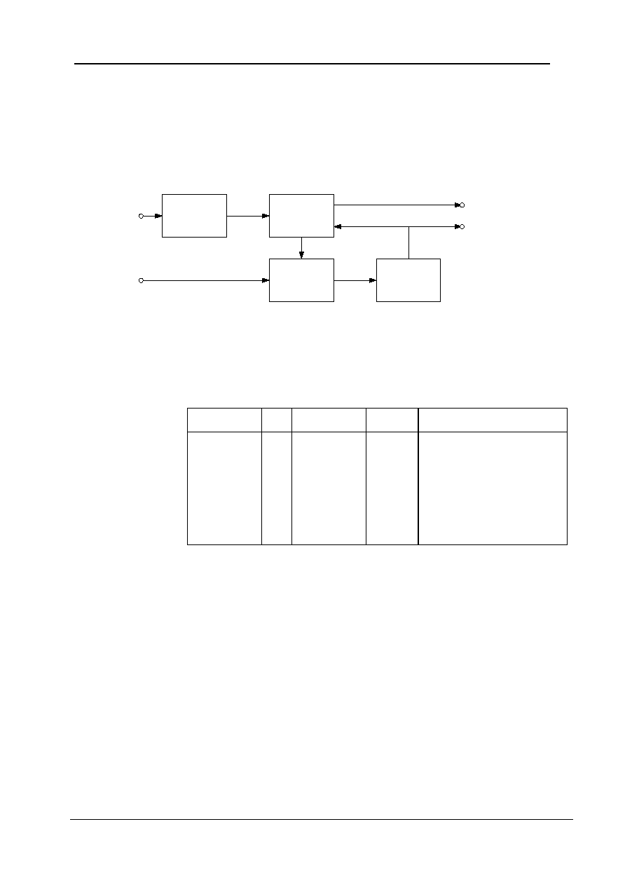
Product Preview
WM8777
w
PP Rev 1.94 November 2004
43
S/PDIF DATA/CLOCK RECOVERY
The WM8777 uses a patented clock and data recovery scheme that allows an extremely low jitter
bandwidth on the output recovered clock. This is done by isolating the clock and data recovery
systems.
The data is recovered and stored in a buffer which modifies the frequency of the recovered clock via
a filter. This filter controls the jitter bandwidth using the register value FPLL.
Data
recovery
Buffer
Filter
Clock
recovery
SPDIF in
FPLL
SPDIF out
Clock out
Figure 24 S/PDIF Data and Clock Recovery System
The jitter bandwidth affects the rate at which the clock can change to track the incoming data rate,
resulting in a slower tracking time as FPLL is increased. Note that this effect is only apparent on
slowly changing input frequencies. Input signals that change frequency by a significant amount, i.e.
data rate changes, will cause the system to lose lock and to enter a quick tracking mode which will
open the filter bandwidth out to the maximum.
Table 30 lists the cut-off frequencies for the different values of FPLL.
REGISTER
ADDRESS
BIT LABEL
DEFAULT DESCRIPTION
(42h)
S/PDIF
Data/Clock
Recovery
5:3
FPLL[2:0]
111
-3dB LPF Cut-Off
000 = Invalid
001 = 28.84Hz
010 = 14.92Hz
011 = 7.46Hz
100 = 3.73Hz
101 = 1.87Hz
110 = 0.97Hz
111 = 0.47Hz
Table 30 PLL Frequency Ratio Control

WM8777
Product Preview
w
PP Rev 1.94 November 2004
44
REGISTER
ADDRESS
BIT LABEL
DEFAULT DESCRIPTION
6
MCLKOPEN
0
MCLK pin output enable
0 = MCLK pin is an input
1 = MCLK pin is an output (refer to
MCLKOUTSRC below
(18h)
Primary
Interface Control
(RX)
7
MCLKOUTSRC
0
MCLK pin output source
0 = PLL
1 = Crystal clock output.
(34h)
PLL Control 1
8:0 PLL_K[8:0]
121
(Hex)
(35h)
PLL Control 2
8:0 PLL_K[17:9]
17E
(Hex)
3:0 PLL_K[21:18]
D(Hex)
Fractional (K) part of PLL
input/output frequency ratio (treat as
one 22-digit binary number).
4
CLKOUTSRC
0
CLKOUT pin source:-
0 = PLL clock output
1 = Crystal clock output.
6
PLL2DAC
0
DAC clock source
0 = MCLK pin
1 = PLL clock
7
PLL2ADC
0
ADC clock source
0 = MCLK or ADCMLCK pin
1 = PLL clock
(36h)
PLL Control 3
8
PLL2TX
1
S/PDIF TX clock source
0 = MLCK or ADCMCLK pin
1 = PLL clock
0
PLLPD
1
0 = Enable PLL
1 = Disable PLL
1
POSTSCALE
0
0 = no post scale
1= divide PLL by 2 after PLL
2
FRAC_EN
0
0 = Integer N only PLL
1 = Integer N and Fractional K PLL
3
PRESCALE
0
0 = no pre-scale
1 = divide MCLK by 2 prior to PLL
(37h)
PLL Control 4
8:4
PLL_N[4:0]
00000
Integer (N) divisor part of PLL
input/output frequency ratio. Use
values greater than 5 and less than
13.
(40h)
S/PDIF
Receiver
Input Selector
8
ADCCLKSRC
0
ADC clock source
0 = ADCMCLK is from MCLK pin
and ADCPBCLK is from PBCLK pin.
1 = ADCMCLK is from GPIO1, and
ADCPBCLK is from GPIO2.(Note
that when in this mode RXINSEL
must not be set to 01 or 10)
Table 31 PLL Frequency Ratio Control
Note: MCLKOPEN should not be toggled if any part of the WM8777 is actively using
MCLK as its clock source.

Product Preview
WM8777
w
PP Rev 1.94 November 2004
45
The PLL performs best when f
2
is around 90MHz. Its stability peaks at N=8. Some example settings are shown below.
XTALC
LK
(MHz)
(F1)
DESIRED
OUTPUT
(MHz)
F2
(MHz)
PRE
SCALE
POST
SCALE
R N
(Hex)
K
(Hex)
11.91 11.2896 90.3168 0
1 7.5833 7 25545C
11.91
12.288
98.304 0
1 8.2539 8 103FF6
12 11.2896
90.3168 0
1 7.5264 7 21B089
12 12.288
98.304 0
1 8.192 8 C49BA
13 11.2896
90.3168 0
1 6.9474 6 3CA2F4
13 12.288
98.304 0
1 7.5618 7 23F548
14.4 11.2896
90.3168 0
1 6.272 6 116872
14.4 12.288
98.304 0
1 6.8267 6 34E818
19.2 11.2896
90.3168 1
1 9.408 9 1A1CAC
19.2 12.288 98.304 1
1 10.24 A F5C28
19.68
11.2896
90.3168 1
1 9.1785 9 B6D22
19.68
12.288
98.304 1
1 9.9902 9 3F6017
19.8 11.2896
90.3168 1
1 9.1229 9 7DDCA
19.8 12.288
98.304 1
1 9.9297 9 3B8023
24 11.2896
90.3168 1
1 7.5264 7 21B089
24 12.288
98.304 1
1 8.192 8 C49BA
26 11.2896
90.3168 1
1 6.9474 6 3CA2F4
26 12.288
98.304 1
1 7.5618 7 23F548
27 11.2896
90.3168 1
1 6.6901 6 2C2B30
27 12.288
98.304 1
1 7.2818 7 12089E
Table 32 PLL Frequency Examples
S/PDIF TRANSCEIVER FEATURES
∑
IEC-60958 compatible with 32 to 96k frames/s support
∑
Support for Rx and Tx of S/PDIF data
∑
Clock synthesis PLL with reference clock input and low jitter output
∑
Input mux with support for up to 4 S/PDIF inputs
∑
Register controlled Channel Status bit configuration
∑
Register read-back of recovered Channel Status bits and error flags
∑
Detection of non-audio data, sample rate, de-emphasis
∑
Programmable GPO for error flags and frame status flags
An IEC-60958 compatible S/PDIF transceiver is integrated into the WM8777. Operation of the
S/PDIF function may be synchronous or asynchronous to the rest of the digital audio circuits.
The receiver performs data and clock recovery, and sends recovered data either off the chip to an
external DSP (via Primary or Secondary Audio Interfaces), or if the data is audio PCM, it can route
the stereo recovered data to DAC1. The recovered clock may be routed out of the chip onto a pin for
external use, and may be used to clock the internal DAC and ADC circuits as required.
The transmitter generates S/PDIF frames where audio data may be sourced from the ADC, S/PDIF
Receiver, Primary or Secondary Audio Interfaces.
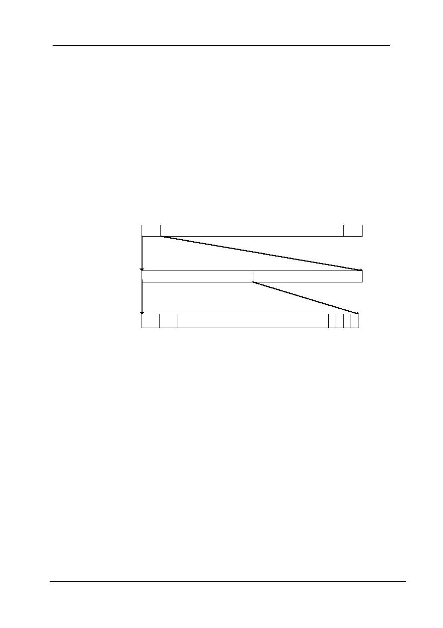
WM8777
Product Preview
w
PP Rev 1.94 November 2004
46
S/PDIF FORMAT
S/PDIF is a serial, bi-phase-mark encoded data stream. An S/PDIF frame consists of two sub-
frames. Each sub-frame is made up of:
∑
Preamble ≠ a synchronization pattern used to identify the start of a 192-frame block or sub-
frame
∑
4-bit Auxiliary Data (AUX) ≠ ordered LSB to MSB
∑
20-bit Audio Data (24-bit when combined with AUX) ≠ ordered LSB to MSB
∑
Validity Bit ≠ a 1 indicates invalid data in that sub-frame
∑
User Bit ≠ over 192-frames, this forms a User Data Block,
∑
Channel Bit ≠ over 192-frames, this forms a Channel Status Block
∑
Parity Bit ≠ used to maintain even parity over the sub-frame(except the preamble)
An S/PDIF Block consists of 192 frames. Channel and User blocks are incorporated within the 192-
frame S/PDIF Block. For Consumer mode (as in the WM8777) only the first 40-frames are used to
make up the Channel and User blocks. Figure 25 illustrates the S/PDIF format.
. . . . . . . . .
Frame
192
Frame
1
Subframe 1
Subframe 2
Sync
preamble
Aux
V
U
C
P
Audio Sample Word
3 4
7 8
27 28
0
31
32 bit
Word
Figure 25 S/PDIF Format
CLOCK RECOVERY AND GENERATION
The circuit comprises data and clock recovery blocks, and a clock synthesis function in the event of
no S/PDIF input. As an integral part of these functions, an accurate, stable, crystal derived master
clock must be input to the WM8777. This clock may be generated using the WM8777 crystal
oscillator circuit, by connecting a suitable crystal across the XIN XOP pins, or else may be applied as
a digital input to the XIN pin. This reference clock input may have any frequency from 10MHz up to
27MHz. When S/PDIF signals are being received, the PLL will recover the audio MCLK at a rate of
256fs or 384fs. In the event of no S/PDIF input, the PLL will continue to synthesise a 128, 256 or
384fs audio clock. If desired the S/PDIF input may be ignored and the PLL instructed to synthesise
any desired audio clock rate (depending upon sample rate). The ratio of this audio clock to the
reference clock frequency is set by programming the required value over the serial interface. Audio
sample rates from 32kHz to 96kHz are supported both by the S/PDIF transceiver and the clock
synthesiser.
The reference clock input should be low jitter, hence it is recommended that a crystal connected to
WM8777 oscillator is used to generate the clock. In this condition very low jitter audio clocks will be
generated, and S/PDIF in-coming clocks will likewise be de-jittered. The WM8777 crystal derived
clock, or the PLL derived audio clock, may then be supplied to external circuits as low jitter clock
references as required.

Product Preview
WM8777
w
PP Rev 1.94 November 2004
47
S/PDIF TRANSMITTER
The S/PDIF transmitter generates the S/PDIF frames, and outputs on the SPDIFOP pin. The audio
data for the frame can be taken from one of four sources, selectable using the TXSRC register. The
transmitter can be powered down using the SPDIFTXD register bit.
REGISTER
ADDRESS
BIT LABEL DEFAULT
DESCRIPTION
2:1
TXSRC[1:0]
00
S/PDIF Transmitter Data Source.
00 = S/PDIF received data.
01 = ADC digital output data.
10 = Secondary Audio Interface received data
11 = Primary Audio Interface Received data.
(41h)
Interface Source
Select
3
TXRXTHRU
0
Only used if TXSRC==00. Configures only the Channel
Bit in the S/PDIF frame.
0 = Channel data equal to recovered channel data.
1 = Channel data taken from channel status registers.
(1Ah)
Powerdown
Control
6 SPDIFTXD
1
SPDIF_TX powerdown
0 = SPDIF_TX enabled
1 = SPDIF_TX disabled
Table 33 S/PDIF Tx Control
The WM8777 also transmits the preamble and VUCP bits (Validity, User Data, Channel Status and
Parity bits).
VALIDITY BIT
Set to 0 (to indicate valid data) ≠ unless TXSRC=00 (S/PDIF receiver), where Validity is set by the
receiver.
USER DATA
Set to 0 as User Data configuration is not supported in the WM8777 ≠ if TXSRC=00 (S/PDIF
receiver) User Data is set by the receiver.
CHANNEL STATUS
The Channel Status bits form a 192-frame block - transmitted at 1 bit per sub-frame. Each sub-frame
forms its own 192-frame block. The WM8777 is a consumer mode device and only the first 40 bits of
the block are used. All data transmitted from the WM8777 is stereo, so the channel status data is
duplicated for both channels. The only exception to this is the channel number bits (23:20) which can
be changed to indicate if the channel is left or right in the stereo image. Bits within this block can be
configured by setting the Channel Bit Control registers (see Tables 28-32 ). If TXSRC is the S/PDIF
receiver, the Channel bits are transmitted with the same values recovered by the receiver ≠ unless
TXRXTHRU is set, in which case they are set by the registers.
Note that the WM8777 expects to receive channel status data in consumer format. The channel
status bits are defined differently for professional mode. The definitions on the following page do not
hold for professional mode.
PARITY BIT
This bit maintains even parity for data as a means of basic error detection. It is generated by the
transmitter.

WM8777
Product Preview
w
PP Rev 1.94 November 2004
48
REGISTER
ADDRESS
BIT LABEL CHANNEL
STATUS
BIT
DEFAULT DESCRIPTION
0
CON/PRO
0
0
0 = Consumer Mode
1 = Professional Mode (not supported by
WM8777)
1
AUDIO_N
1
0
0 = S/PDIF transmitted data is audio PCM.
1 = S/PDIF transmitted data is not audio
PCM.
2
CPY_N
2
0
0 = Transmitted data has copyright asserted.
1 = Transmitted data has no copyright
assertion.
5:3 PREEMPH
[2:0]
5:3
000
000 = Data from Audio interface has no pre-
emphasis.
001 = Data from Audio interface has pre-
emphasis.
010 = Reserved (Audio interface has pre-
emphasis).
011 = Reserved (Audio interface has pre-
emphasis).
All other modes are reserved and should not
be used.
(39h)
S/PDIF
Transmitter
Channel Bit
Control 1
7:6
CHSTMODE
[1:0]
7:6
00
S/PDIF Channel status bits.
00 = Only valid mode for consumer
applications.
All other modes are reserved.
Table 34 S/PDIF Tx Channel Bit Control 1
REGISTER
ADDRESS
BIT LABEL CHANNEL
STATUS
BIT
DEFAULT DESCRIPTION
(3Ah)
S/PDIF
Transmitter
Channel Bit
Control 2
7:0 CATCODE
[7:0]
15:8
00000000
Category Code. Refer to S/PDIF
specification for details.
00h indicates "general" mode.
Table 35 S/PDIF Tx Channel Bit Control 2
REGISTER
ADDRESS
BIT LABEL CHANNEL
STATUS
BIT
DEFAULT DESCRIPTION
3:0 SRCNUM
[3:0]
19:16
0000
Source Number. No definitions are attached
to data. See S/PDIF specification for details.
Channel Number for Subframe 1
CHNUM1
Channel Status Bits[23:20]
00
0000 = Do not use channel
number
01
0001 = Send to Left Channel
10
0010 = Send to Right Channel
5:4 CHNUM1[1:0] 23:20
00
11
0000 = Do not use channel
number
Channel Number for Subframe 2
CHNUM2
Channel Status Bits[23:20]
00
0000 = Do not use channel
number
01
0001 = Send to Left Channel
10
0010 = Send to Right Channel
(3Bh)
S/PDIF
Transmitter
Channel Bit
Control 3
7:6 CHNUM2[1:0]
00
11
0000 = Do not use channel
number
Table 36 S/PDIF Tx Channel Bit Control 3

Product Preview
WM8777
w
PP Rev 1.94 November 2004
49
REGISTER
ADDRESS
BIT LABEL CHANNEL
STATUS
BIT
DEFAULT DESCRIPTION
3:0
FREQ[3:0]
27:24
0001
Sampling Frequency. See S/PDIF
specification for details.
0001 = Sampling Frequency not indicated.
(3Ch)
S/PDIF
Transmitter
Channel Bit
Control 4
5:4
CLKACU[1:0]
29:28
11
Clock Accuracy of Generated clock.
00 = Level II
01 = Level I
10 = Level III
11 = Interface frame rate not matched to
sampling frequency.
Table 37 S/PDIF Tx Channel Bit Control 4
REGISTER
ADDRESS
BIT LABEL CHANNEL
STATUS
BIT
DEFAULT DESCRIPTION
0
MAXPAIFRX_WL
32
1
Maximum Audio sample word length
0 = 20 bits
1 = 24 bits
Audio Sample Word Length.
000 = Word Length Not Indicated
TXPAIFRX_
WL
MAXPAIFR
X_WL==1
MAXPAIFR
X_WL==0
001
20 bits
16 bits
010
22 bits
18 bits
100
23 bits
19 bits
101
24 bits
20 bits
110
21 bits
17 bits
3:1
TXPAIFRX_WL
[2:0]
35:33 101
All other combinations reserved
(3Dh)
S/PDIF
Transmitter
Channel Bit
Control 5
7:4 ORGSAMP
[3:0]
39:36
0000
Original Sampling Frequency. See S/PDIF
specification for details.
0000 = original sampling frequency not
indicated
Table 38 S/PDIF Tx Channel Bit Control 5

WM8777
Product Preview
w
PP Rev 1.94 November 2004
50
S/PDIF RECEIVER
INPUT SELECTOR
The S/PDIF receiver has one dedicated input, SPIN. There are three other pins which can be
configured as either S/PDIF inputs or general purpose outputs (GPOs). The four S/PDIF inputs go
into a 4:1 mux, allowing one input to go to the S/PDIF receiver for decoding. The S/PDIF receiver can
be powered down using the SPDIFRXD register bit.
Table 39 S/PDIF Rx Input Selection register
AUDIO DATA HANDLING
The S/PDIF receiver recovers the data and VUCP bits from each sub-frame. If the S/PDIF input data
is in PCM format the data can be internally routed to the stereo data input of DAC1. The WM8777
can detect when the data is not in PCM format and will automatically mute the DAC. See Non-Audio
Detection for more detail.
The received data can also be output over the Audio interfaces in any of the data formats supported.
This can be done while simultaneously using DAC1 for playback. The received data may also be re-
transmitted over SPDIFOP.
USER DATA
The WM8777 can output recovered user data received over the GPIO pins. See Table 48 for General
Purpose Pin control.
CHANNEL STATUS DATA
The channel status bits are recovered from the incoming data stream and are used to control various
functions of the device. The recovered MAXPAIFRX_WL and PAIFRX_WL bits are used to truncate
the recovered 24-bit audio word to so that only the appropriate numbers of bits are used by the other
interfaces (except the S/PDIF transmitter which always sees the full 24-bit recovered word).
Should the recovered DEEMPH Channel-bit be set, and DAC1 is used for playback, the de-emphasis
filter is activated for that DAC.
It is assumed that the channel status is stereo and hence only channel 1 data is read. The channel
status data is stored in 5 read-only registers which can be read back over the serial interface (see
Serial Interface Readback). When the channel status data has been recovered and stored in
registers, the CSUD (Channel Status UpDate) bit goes high to indicate that the registers are ready for
readback. It will go low again when the first sub-frame of data from the next block is received. CSUD
can be output to one of the GPIO pins.
REGISTER
ADDRESS
BIT LABEL DEFAULT
DESCRIPTION
0
SPDINMODE
0
Selects the input circuit type for the S/PDIF input
0 = Normal CMOS input
1 = Comparator input. Compatible with 200mV AC
coupled consumer S/PDIF input signals.
(40h)
S/PDIF
Receiver
Input Selector
5:4
RXINSEL[1:0]
00
S/PDIF Receiver input mux select. Note that the general
purpose inputs must be configured using GPIOxOP to
be either CMOS or comparator inputs if selected by
RXINSEL.
00 = S/PDIF_IN1
01 = S/PDIF_IN2 (GPIO1)
10 = S/PDIF_IN3 (GPIO2)
11 = S/PDIF_IN4 (GPIO3)

Product Preview
WM8777
w
PP Rev 1.94 November 2004
51
The register descriptions for the channel status bits are given below. Note that the descriptions
below refer to consumer mode. The WM8777 may give erroneous behaviour if professional format
data is input.
REGISTER
ADDRESS
BIT LABEL CHANNEL
STATUS
BIT
DESCRIPTION
0
CON/PRO
0
0 = Consumer Mode
1 = Professional Mode
The WM8777 is a consumer mode device.
Detection of professional mode may give
erroneous behaviour.
1
AUDIO_N
1
Recovered S/PDIF Channel status bit 1.
0 = Data word represents audio PCM
samples.
1 = Data word does not represent audio
PCM samples.
2
CPY_N
2
0 = Copyright is asserted for this data.
1 = Copyright is not asserted for this data.
3
PREEMPH
3
0 = Recovered S/PDIF data has no pre-
emphasis.
1 = Recovered S/PDIF data has pre-
emphasis.
(4Ch)
S/PDIF
Receiver
Channel
Status
Register 1
(read-only)
5:4
Reserved
5:4
Reserved for additional de-emphasis modes.
Table 40 S/PDIF Rx Channel Status Register 1
REGISTER
ADDRESS
BIT LABEL CHANNEL
STATUS
BIT
DESCRIPTION
(4Dh)
S/PDIF
Receiver
Channel
Status
Register 2
(read-only)
7:0 CATCODE
[7:0]
15:8
Category Code. Refer to S/PDIF
specification for details.
00h indicates "general" mode.
Table 41 S/PDIF Rx Channel Status Register 2
REGISTER
ADDRESS
BIT LABEL CHANNEL
STATUS
BIT
DESCRIPTION
3:0 SRCNUM
[3:0]
19:16
Indicates number of S/PDIF source.
(4Eh)
S/PDIF
Receiver
Channel
Status
Register 3
(read-only)
7:4
CHNUM1[3:0]
23:20
Channel number for channel 1.
0000 = Take no account of channel number
(channel 1 defaults to left DAC)
0001 = channel 1 to left channel
0010 = channel 1 to right channel
Table 42 S/PDIF Rx Channel Status Register 3

WM8777
Product Preview
w
PP Rev 1.94 November 2004
52
REGISTER
ADDRESS
BIT LABEL CHANNEL
STATUS
BIT
DESCRIPTION
3:0
FREQ[3:0]
27:24
Sampling Frequency. See S/PDIF
specification for details.
0001 = Sampling Frequency not indicated.
(4Fh)
S/PDIF
Receiver
Channel
Status
Register 4
(read-only)
5:4
CLKACU[1:0]
29:28
Clock Accuracy of received clock.
00 = Level II
01 = Level I
10 = Level III
11 = Interface frame rate not matched to
sampling frequency.
Table 43 S/PDIF Rx Channel Status Register 4
REGISTER
ADDRESS
BIT LABEL CHANNEL
STATUS
BIT
DESCRIPTION
0
MAXPAIFRX_WL
32
Maximum Audio sample word length
0 = 20 bits
1 = 24 bits
Audio Sample Word Length.
000: Word Length Not Indicated
RXPAIFRX_
WL
MAXPAIFR
X_WL==1
MAXPAIFR
X_WL==0
001
20 bits
16 bits
010
22 bits
18 bits
100
23 bits
19 bits
101
24 bits
20 bits
110
21 bits
17 bits
3:1 RXPAIFRX_WL
[2:0]
35:33
All other combinations are reserved and may
give erroneous operation. Data will be
truncated internally when these bits are set.
(50h)
S/PDIF
Receiver
Channel
Status
Register 5
(read-only)
7:4 ORGSAMP
[3:0]
39:36
Original Sampling Frequency. See S/PDIF
specification for details.
0000 = original sampling frequency not
indicated
Table 44 S/PDIF Rx Channel Status Register 5

Product Preview
WM8777
w
PP Rev 1.94 November 2004
53
ERROR HANDLING
Several kinds of error can be reported when decoding the incoming data. The error bits are written to
a read-only register which can be read back by the user over the serial interface. Reading back this
register will reset it.
REGISTER
ADDRESS
BIT LABEL DEFAULT
DESCRIPTION
0
UNLOCK
0
PLL Unlock signal.
0 = PLL is locked to incoming S/PDIF stream.
1 = PLL is not locked to the incoming S/PDIF stream.
1
VALIDITY
0
V bit from S/PDIF input stream.
0 = Data word is valid.
1 = Data word is not valid.
2
PARITYERR
0
Even Parity check.
0 = No Parity errors detected.
1 = Parity error detected.
3
BIP
0
Biphase coding of S/PDIF input stream.
0 = Biphase Coding is correct.
1 = Biphase Coding error detected.
4
AUDIO_N
0
Received Channel status bit 1 has changed.
0 = Normal running.
1 = Change on AUDIO_N.
5
PCM_N
0
PCM_N bit has changed
0 = Normal running.
1 = Change on PCM_N.
6
CPY_N
0
Received Channel status bit 2 has changed.
0 = Normal running.
1 = Change on CPY_N.
(4Bh)
S/PDIF
Receiver
Error Register
(read-only)
7
SPDIF_MODE
0
S/PDIF mode change.
0: Normal running
1: Change in S/PDIF frequency mode detected.
Table 45 S/PDIF Rx Error Status Register
When an error is detected the INT signal is set high. This is a logical OR of the error bits which can
be output to a GPIO (GPIO1 by default). Error bits can be masked off by setting the mask register. If
an error bit is masked off then that error will not be written to the error register and will not cause a
change on INT.
UNLOCK, VALIDITY, PARITY and BIP generate an interrupt when they go from low to high. These
bits are sticky, i.e. the interrupt will remain until the user reads back the register to clear it. AUDIO_N,
PCM_N, CPY_N and SPDIF_MODE will generate an interrupt on any change in status. The user
can then determine the status of these bits by reading back the S/PDIF status register.

WM8777
Product Preview
w
PP Rev 1.94 November 2004
54
REGISTER
ADDRESS
BIT LABEL DEFAULT
DESCRIPTION
0
AUDIO_N
Received Channel status bit 1
0 = Data word represents audio PCM samples.
1 = Data word does not represent audio PCM samples.
1
PCM_N
Detects non-audio data from a 96-bit sync code, as
defined in IEC-61937.
0 = Sync code not detected.
1 = Sync code detected ≠ received data is not audio
PCM.
2
CPY_N
Recovered S/PDIF Channel status bit 2.
0 = Copyright is asserted for this data.
1 = Copyright is not asserted for this data.
Note this signal is inverted and will cause an interrupt on
logic 0.
(51h)
S/PDIF Status
Register
(read-only)
4:3
SPDIF_MODE
S/PDIF frequency mode.
00: Mode not supported
01: 88-96KHz
10: 44-48KHz
11: 32KHz
Table 46 S/PDIF Rx Status Register
Should the incoming S/PDIF sub-frame contain a PARITY error or a BIP error, it is assumed the sub-
frame has become corrupted. These errors would normally be flagged, but if the error bits have been
masked, the WM8777 will instead overwrite the recovered frame (i.e. both sub-frames) with either
all-zeros or the last data sample (depending on how FILLMODE has been set). When the flags are
unmasked and an error is detected, the data is allowed to pass, albeit still corrupted.
Similarly, if VALIDITY is detected as 1, it is assumed the data within the S/PDIF frame is invalid. If
VALIDITY is masked, then data is overwritten depending on FILLMODE, else VALIDITY is flagged
and the (invalid) data is allowed to pass. (Note1: ALWAYSVALID must be set to 0, else the
recovered VALIDITY bit will be ignored). (Note 2: For the S/PDIF Receiver to S/PDIF transmitter
path, only masked VALIDITY errors will cause data to be overwritten ≠ PARITY and BIP errors have
no effect).
REGISTER
ADDRESS
BIT LABEL DEFAULT
DESCRIPTION
(49h)
S/PDIF
Receiver
Error Mask
7:0
MASK[7:0]
0000000
When a lag is masked, it does not update the Error
Register or contribute to the interrupt pulse. 0 =
unmask, 1 = mask.
MASK[0] = mask control for UNLOCK
MASK[1] = mask control for VALIDITY
MASK[2] = mask control for PARITYERR
MASK[3] = mask control for BIP
MASK[4] = mask control for AUDIO_N
MASK[5] = mask control for PCM_N
MASK[6] = mask control for CPY_N
MASK[7] = mask control for SPDIF_MODE
6 FILLMODE
0
Determines what SPDIF_RX should do if the validity bit
indicates invalid data:
0 = Data from SPDIF_RX remains static at last valid
sample.
1 = Data from SPDIF_RX is output as all zeros.
(40h)
S/PDIF
Receiver
Input Selector
7 ALWAYSVALID
0
Used to override the recovered validity bit.
0 = Use validity bit.
1 = Ignore validity bit.
Table 47 S/PDIF Rx Error Mask Register

Product Preview
WM8777
w
PP Rev 1.94 November 2004
55
The circuit for dealing with UNLOCK, VALIDITY, PARITY and BIP errors is shown in Figure 26.
INT
Serial
Interface
Readback
Mask bit[0/1/2/3]
Error bit[0/1/2/3]
RegisterReadDone
SET
CLR
Set Domiant
Figure 26 S/PDIF Error Handling Circuit for UNLOCK, VALIDITY, PARITY and BIP Errors
NON-AUDIO DETECTION
Non-Audio data is indicated by the AUDIO_N and PCM_N bits. AUDIO_N is recovered from the
Channel Status block. PCM_N is set on detection of the 96-bit IEC-61937 non-audio data sync code,
embedded in the data section of the S/PDIF frame. When either the AUDIO_N or PCM_N bits are set
in the error register, and DAC1 is being used for playback, the DAC will be muted automatically using
the softmute feature. As described above, any change on AUDIO_N or PCM_N will cause an
interrupt to be generated. If the MASK register bit for AUDIO_N or PCM_N is set, then that signal will
not generate an interrupt but will still mute the DAC.
If non-audio data is detected and the DAC has been muted, the user must ensure that audio data is
being input, then clear the error register. The mute on the DAC will be removed when the WM8777
detects that audio data is being received.
GENERAL PURPOSE INPUT AND OUTPUT (GPIO) PINS
The WM8777 has four pins which can be additionally configured as GPIOs, using the registers
shown in Table 48. The GPIO pins can be used to output control and status data decoded by the
S/PDIF receiver
REGISTER
ADDRESS
BIT LABEL DEFAULT
DESCRIPTION
3:0 GPIO1OP[3:0]
0000
(47h)
GPIO
Control 1
7:4 GPIO2OP[3:0]
0001
3:0 GPIO3OP[3:0]
0010
(48h)
GPIO
Control 2
7:4
GPOMODEOP
[3:0]
1010
0000 = INT
0001 = V - Validity
0010 = U - User Data bit
0011 = C - Channel Status Data
0100 = P - Parity bit
0101 = Non-audio (AUDIO_N || PCM_N)
0110 = UNLOCK
0111 = CSUD (Channel Status Registers Updated)
1000 = Zero Flag 1 output
1001 = Zero Flag 2 output
1010 = GPIOx set as S/PDIF input (standard CMOS
input buffer). Not valid for GPOMODE.
1011 = GPIOx set as S/PDIF input (`comparator' input
for AC coupled consumer S/PDIF signals). Not valid for
GPOMODE.
1100 = Sub Frame clock (1 = sub-frame1, 0 = sub-
frame2)
1101 = Start of Block signal
Table 48 GPIO Control Registers
WM8777
Product Preview
w
PP Rev 1.94 November 2004
56
DAC CONTROL REGISTERS
DAC INPUT CONTROL
The primary audio interface has a separate input pin for each stereo DAC. Any input pin can be
routed to any DAC using the DACxSEL register bits.
REGISTER ADDRESS
BIT
LABEL
DEFAULT
DESCRIPTION
1:0 DAC1SEL
[1:0]
00
3:2
DAC2SEL
[1:0]
01
5:4
DAC3SEL
[1:0]
10
(38h)
DAC Digital Input
Selector
7:6
DAC4SEL
[1:0]
11
DAC digital input select.
00 = DAC takes data from
PDATAIP1
01 = DAC takes data from
PDATAIP2
10 = DAC takes data from
PDATAIP3
11 = DAC takes data from
PDATAIP4
Table 49 DAC Input Select Register
MUTE MODES
The WM8777 has individual mutes for each of the four DAC channels. Setting MUTE for a channel
will apply a `soft' mute to the input of the digital filters of the channel muted. DMUTE[0] mutes DAC
channel 1, DMUTE[1] mutes DAC channel 2, DMUTE[2] mutes DAC channel 3 and DMUTE[3] mutes
DAC channel 4. Setting the MUTEALL register bit will apply a 'soft' mute to the input of all the DAC
digital filters
REGISTER ADDRESS
BIT
LABEL
DEFAULT
DESCRIPTION
3:0
DMUTE[3:0] 0000 DAC channel soft mute
enables:
DMUTE[0] = 1, enable
softmute on DAC1.
DMUTE[1] = 1, enable
softmute on DAC2.
DMUTE[2] = 1, enable
softmute on DAC3.
DMUTE[3] = 1, enable
softmute on DAC4.
(16h)
Mute Control
4 MUTEALL
0
DAC channel master soft mute.
Mutes all DAC channels:
0 = disable softmute on all
DACs.
1 = enable softmute on all
DACs.
Table 50 Mute Registers

Product Preview
WM8777
w
PP Rev 1.94 November 2004
57
Figure 27 Application and Release of Soft Mute
Figure 27 shows the application and release of MUTE whilst a full amplitude sinusoid is being played
at 48kHz sampling rate. When MUTE (lower trace) is asserted, the output (upper trace) begins to
decay exponentially from the DC level of the last input sample. The output will decay towards V
MID
with a time constant of approximately 64 input samples. If MUTE is applied to all channels for 1024
or more input samples the DAC will be muted if IZD is set. When MUTE is de-asserted, the output
will restart immediately from the current input sample.
Note that all other means of muting the DAC channels: setting the PL[3:0] bits to 0, setting the
PDWN bit or setting attenuation to 0 will cause much more abrupt muting of the output.
The Record outputs may be enabled by setting RECEN, where RECEN enables the REC1L and
REC1R outputs.
REGISTER ADDRESS
BIT
LABEL
DEFAULT
DESCRIPTION
6:5
RECLEN
00
RECL Output Enable
00 = REC output muted
01 = REC output ADCL
10 = REC output DAC1L
(16h)
Mute Control
8:7
RECREN
00
RECR Output Enable
00 = REC output muted
01 = REC output ADCR
10 = REC output DAC1R
Table 51 REC Enable Registers
-2.5
-2
-1.5
-1
-0.5
0
0.5
1
1.5
0
0.001
0.002
0.003
0.004
0.005
0.006
Time(s)

WM8777
Product Preview
w
PP Rev 1.94 November 2004
58
ZERO FLAG OUTPUT
The WM8777 has a zero detect circuit for each DAC channel which detects when 1024 consecutive
zero samples have been input. Two zero flag outputs (ZFLAG1 and ZFLAG2) may be output through
the GPIO pins which may then be used to control external muting circuits. A `1' on ZFLAG1 or
ZFLAG2 indicates a zero detect. The zero detect may also be used to automatically enable the DAC
mute by setting IZD. The zero flag output may be disabled by setting DZFM to 0000. The zero flag
signal for a DAC channel will only be a `1' if that channel is disabled as an input to the output
summing stage.
REGISTER ADDRESS
BIT
LABEL
DEFAULT
DESCRIPTION
(17h)
DAC Control
7:4
DZFM[3:0] 0000 Selects the ouput for ZFLG1 and
ZFLG2 pins (see Table 53).
1 = indicates 1024 consecutive
zero input samples on the
channels selected
0 = indicates at least one of
selected channels has non zero
sample in last 1024 inputs
Table 52 DZFM Register
DZFM[3:0] ZFLAG1
ZFLAG2
0000
Zero flag disabled
Zero flag disabled
0001
All channels zero
All channels zero
0010
Left channels zero
Right channels zero
0011
Channel 1 zero
Channels 2-4 zero
0100
Channel 1 zero
Channel 2 zero
0101
Channel 1 zero
Channel 3 zero
0110
Channel 1 zero
Channel 4 zero
0111
Channel 2 zero
Channel 3 zero
1000
Channel 2 zero
Channel 4 zero
1001
Channel 3 zero
Channel 4 zero
1010
Channels 1-3 zero
Channel 4 zero
1011
Channel 1 zero
Channels 2 and 3
zero
1100
Channel 1 left zero
Channel 1 right zero
1101
Channel 2 left zero
Channel 2 right zero
1110
Channel 3 left zero
Channel 3 right zero
1111
Channel 4 left zero
Channel 4 right zero
Table 53 Zero Flag Output Select
INFINITE ZERO DETECT
Setting the IZD register bit will enable the internal infinite zero detect function:
REGISTER ADDRESS
BIT
LABEL
DEFAULT
DESCRIPTION
(15h)
DAC Attenuation Control
2 IZD
0 Infinite zero detection circuit control
and automute control
0 = Infinite zero detect automute
disabled
1 = Infinite zero detect automute
enabled
Table 54 IZD Register
With IZD enabled, applying 1024 consecutive zero input samples each stereo channel will cause that
stereo channels outputs to be muted. Mute will be removed as soon as any channel receives a non-
zero input.
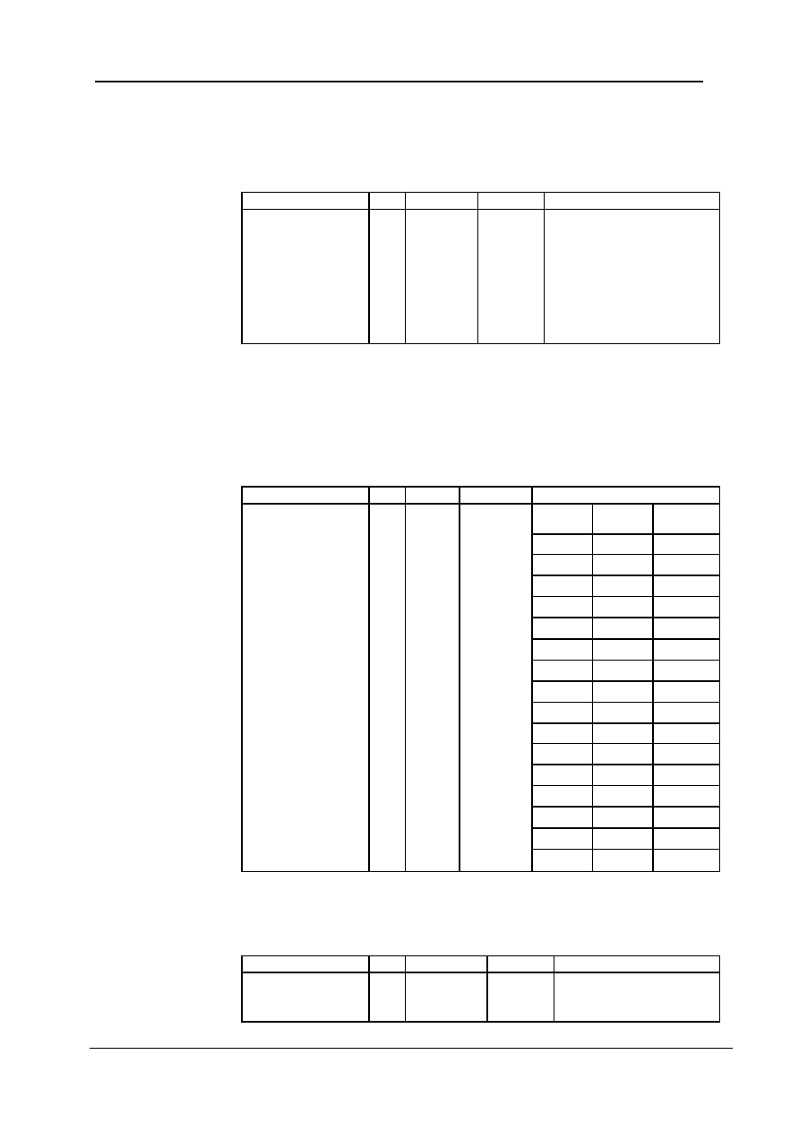
Product Preview
WM8777
w
PP Rev 1.94 November 2004
59
DE-EMPHASIS MODE
A digital De-emphasis filter may be applied to each DAC channel. The De-emphasis filter for each
stereo channel is enabled under the control of DEEMP[3:0]. DEEMP[0] enables the de-emphasis
filter for channel 1, DEEMP[1] enables the de-emphasis filter for channel 2, DEEMP[2] enables the
de-emphasis filter for channel 3 and DEEMP[3] enables the de-emphasis filter for channel 4.
REGISTER ADDRESS
BIT
LABEL
DEFAULT
DESCRIPTION
(17h)
DAC Control
3:0
DEEMP[3:0]
0000
De-emphasis mode select:
DEEMPH[0] = 1, enable De-
emphasis on DAC1.
DEEMPH[1] = 1, enable De-
emphasis on DAC2.
DEEMPH[2] = 1, enable De-
emphasis on DAC3.
DEEMPH[3] = 1, enable De-
emphasis on DAC4.
Table 55 De-emphasis Register
Refer to Figure 37, Figure 38, Figure 39, Figure 40, Figure 41 and Figure 42 for details of the De-
Emphasis modes at different sample rates.
DAC OUTPUT CONTROL
The DAC output control word determines how the left and right inputs to the audio Interface are
applied to the left and right DACs:
REGISTER ADDRESS
BIT
LABEL
DEFAULT
DESCRIPTION
PL[3:0]
Left
Output
Right
Output
0000 Mute Mute
0001 Left Mute
0010 Right Mute
0011 (L+R)/2 Mute
0100 Mute Left
0101 Left Left
0110 Right Left
0111 (L+R)/2 Left
1000 Mute Right
1001 Left Right
1010 Right Right
1011 (L+R)/2 Right
1100 Mute (L+R)/2
1101 Left (L+R)/2
1110 Right (L+R)/2
(15h)
DAC Attenuation Control
8:5 PL[3:0]
1001
1111 (L+R)/2 (L+R)/2
Table 56 DAC Attenuation Register (PL)
DAC OVERSAMPLING RATE SELECT
Control bit DACOSR allow the user to select the DAC internal signal processing oversampling rate.
Operation is described in Table 18 and Table 19.
REGISTER ADDRESS
BIT
LABEL
DEFAULT
DESCRIPTION
(19h)
DAC Oversampling
Rate Select
3
DACOSR
0
DAC oversampling rate select
0: 128x oversampling
1: 64x oversampling
Table 57 DAC Oversampling Rate

WM8777
Product Preview
w
PP Rev 1.94 November 2004
60
ATTENUATOR CONTROL MODE
Setting the ATC register bit causes the left channel attenuation settings to be applied to both left and
right channel DACs from the next audio input sample. No update to the attenuation registers is
required for ATC to take effect. When the ATC register bit is unset the right channel gain is applied
form the new audio input sample.
REGISTER ADDRESS
BIT
LABEL
DEFAULT
DESCRIPTION
(15h)
DAC Attenuation Control
1
DACATC
0
Attenuator Control
0 = All DACs use attenuations as
programmed.
1 = Right channel DACs use
corresponding left DAC attenuations
Table 58 DAC Attenuation Register (DACATC)
ANALOGUE VOLUME CONTROL
The DAC volume may be adjusted independently in both the analogue and digital domain using
separate volume control registers.
REGISTER
ADDRESS
BIT LABEL DEFAULT
DESCRIPTION
6:0
FRONTLA
[6:0]
1101011
(0dB)
Analogue Attenuation control for FRONTL in 1dB steps. See Table
60.
7
FRONTLZCEN
0
FRONTL zero cross detect enable
0 = zero cross disabled
1 = zero cross enabled
(00h)
Analogue
Attenuation
FRONTL
8
UPDATE Not
latched Controls simultaneous update of all Analogue Attenuation Latches
0 = Store FRONTL in intermediate latch (no change to output)
1 = Store FRONTL and update attenuation on all channels.
6:0
FRONTRA
[6:0]
1101011
(0dB)
Analogue Attenuation control for FRONTR in 1dB steps. See Table
60.
7
FRONTRZCEN
0
FRONTR zero cross detect enable
0 = zero cross disabled
1 = zero cross enabled
(01h)
Analogue
Attenuation
FRONTR
8
UPDATE Not
latched Controls simultaneous update of all Analogue Attenuation Latches
0 = Store FRONTR in intermediate latch (no change to output)
1 = Store FRONTR and update attenuation on all channels.
6:0
CNTRA
[6:0]
1101011
(0dB)
Analogue Attenuation control for CNTR in 1dB steps. See Table 60.
7
CNTRZCEN 0 CNTR zero cross detect enable
0 = zero cross disabled
1 = zero cross enabled
(02h)
Analogue
Attenuation CNTR
8
UPDATE Not
latched Controls simultaneous update of all Analogue Attenuation Latches
0 = Store CNTR in intermediate latch (no change to output)
1 = Store CNTR and update attenuation on all channels.
6:0
LFEA
[6:0]
1101011
(0dB)
Analogue Attenuation control for LFE in 1dB steps. See Table 60.
7
LFEZCEN 0 LFE zero cross detect enable
0 = zero cross disabled
1 = zero cross enabled
(03h)
Analogue
Attenuation
LFE
8
UPDATE Not
latched Controls simultaneous update of all Analogue Attenuation Latches
0 = Store LFE in intermediate latch (no change to output)
1 = Store LFE and update attenuation on all channels.

Product Preview
WM8777
w
PP Rev 1.94 November 2004
61
REGISTER
ADDRESS
BIT LABEL DEFAULT
DESCRIPTION
6:0 SURLA
[6:0]
1101011
(0dB)
Analogue Attenuation control for SURL in 1dB steps. See Table 60.
7
SURLZCEN 0 SURL zero cross detect enable
0 = zero cross disabled
1 = zero cross enabled
(04h)
Analogue
Attenuation
SURL
8
UPDATE Not
latched Controls simultaneous update of all Analogue Attenuation Latches
0 = Store SURL in intermediate latch (no change to output)
1 = Store SURL and update attenuation on all channels.
6:0 SURRA
[6:0]
1101011
(0dB)
Analogue Attenuation control for SUR Right in 1dB steps.
7
SURRZCEN 0 SURR zero cross detect enable
0 = zero cross disabled
1 = zero cross enabled
(05h)
Analogue
Attenuation
SURR
8
UPDATE Not
latched Controls simultaneous update of all Analogue Attenuation Latches
0 = Store SURR in intermediate latch (no change to output)
1 = Store SURR and update attenuation on all channels.
6:0
AUXLA[6:0] 1101011
(0dB)
Analogue Attenuation control for AUXL in 1dB steps. See Table 60.
7
AUXLZCEN 0 AUXL zero cross detect enable
0 = zero cross disabled
1 = zero cross enabled
(06h)
Analogue
Attenuation AUXL
8
UPDATE Not
latched Controls simultaneous update of all Analogue Attenuation Latches
0 = Store AUXL in intermediate latch (no change to output)
1 = Store AUXL and update attenuation on all channels.
6:0
AUXRA[6:0] 1101011
(0dB)
Analogue Attenuation control for AUXR in 1dB steps. See Table 60.
7
AUXRZCEN 0 AUXR zero cross detect enable
0 = zero cross disabled
1 = zero cross enabled
(07h)
Analogue
Attenuation AUXR
8
UPDATE Not
latched Controls simultaneous update of all Analogue Attenuation Latches
0 = Store AUXR in intermediate latch (no change to output)
1 = Store AUXR and update attenuation on all channels.
6:0
HPLA[6:0] 1101011
(0dB)
Analogue Attenuation control for HPHONEL in 1dB steps. See Table
60.
7
HPLZCEN 0 HPHONEL zero cross detect enable
0 = zero cross disabled
1 = zero cross enabled
(08h)
Analogue
Attenuation
HPHONEL
8
UPDATE Not
latched Controls simultaneous update of all Analogue Attenuation Latches
0 = Store HPHONEL in intermediate latch (no change to output)
1 = Store HPHONEL and update attenuation on all channels.
6:0
HPRA[6:0] 1101011
(0dB)
Analogue Attenuation control for HPHONER in 1dB steps. See Table
60.
7
HPRZCEN 0 HPHONER zero cross detect enable
0 = zero cross disabled
1 = zero cross enabled
(09h)
Analogue
Attenuation
HPHONER
8
UPDATE Not
latched Controls simultaneous update of all Analogue Attenuation Latches
0 = Store HPHONER in intermediate latch (no change to output)
1 = Store HPHONER and update attenuation on all channels.
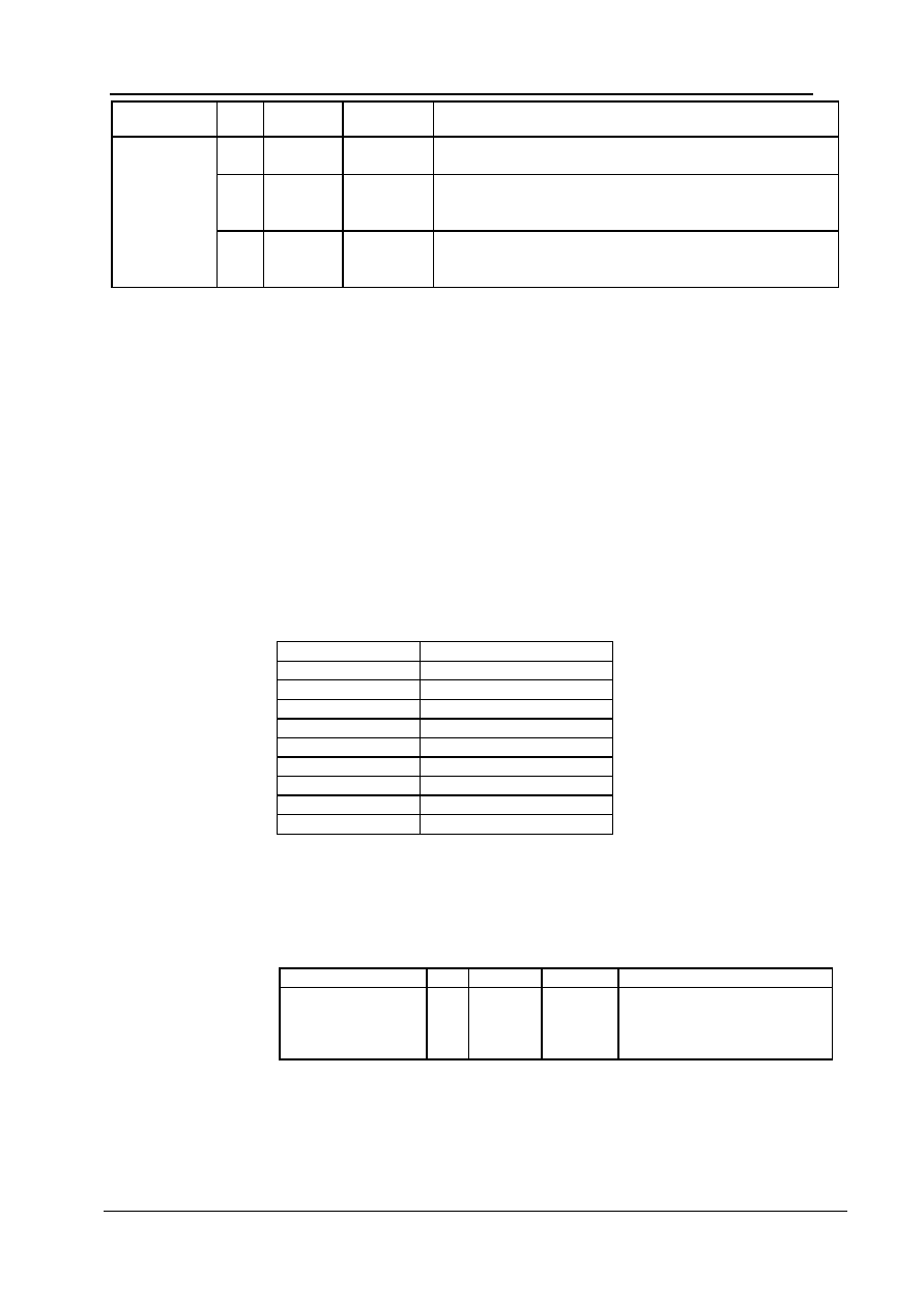
WM8777
Product Preview
w
PP Rev 1.94 November 2004
62
REGISTER
ADDRESS
BIT LABEL DEFAULT
DESCRIPTION
6:0
MASTA[6:0] 1101011
(0dB)
Analogue Attenuation control for all DAC gains in 1dB steps. See
Table 60.
7
MZCEN 0
Master zero cross detect enable
0 = zero cross disabled
1 = zero cross enabled
(0Ah)
Analogue
Attenuation
Master
(all channels)
8
UPDATE Not
latched Controls simultaneous update of all Analogue Attenuation Latches
0 = Store gains in intermediate latch (no change to output)
1 = Store gains and update attenuation on all channels.
Table 59 Analogue Attenuation Registers
Each analogue output channel volume can be controlled digitally in an analogue volume stage after
the DAC. Attenuation is 0dB by default but can be set between +20dB and ≠100dB in 1dB steps
using the 7 Attenuation control words. All attenuation registers are double latched allowing new
values to be pre-latched to several channels before being updated synchronously. Setting the
UPDATE bit on any attenuation write will cause all pre-latched values to be immediately applied to
the DAC channels. A master attenuation register is also included, allowing all volume levels to be set
to the same value in a single write.
Note: The UPDATE bit is not latched. If UPDATE=0, the Attenuation value will be written to the pre-
latch but not applied to the relevant ouptut. If UPDATE=1, all pre-latched values will be applied from
the next input sample. Writing to MASTA[6:0] overwrites any values previously sent to FRONTL[6:0],
CNTR[6:0], SURL[6:0], AUXL[6:0], FRONTR[6:0], LFE[6:0], SURR[6:0], AUXR[6:0].
Register bits FRONTL and FRONTR control the left and right channel attenuation of the Front
channels. Register bits CNTR and LFE control the left and right channel attenuation of CNTR and
LFE respectively. Register bits SURL and SURR control the left and right channel attenuation of
surround channels. Register bits AUXL and AUXR control the left and right channel attenuation of the
auxiliary channel. Register bits MASTA can be used to control attenuation of all channels.
Table 60 shows how the attenuation levels are selected from the 7-bit words.
L/RA
x
[6:0] ATTENUATION
LEVEL
00(hex) -
dB (mute)
: :
06(hex) -
dB (mute)
07(hex) -100dB
: :
6B(hex) 0dB
(default)
7D(hex) +18dB
7E(hex) +19dB
7F(hex) +20dB
Table 60 Analogue Volume Control Attenuation Levels
In addition a zero cross detect circuit is provided for each analogue output volume under the control
of bit 7 (xZCEN) in each Analogue attenuation register. When ZCEN is set the attenuation values are
only updated when the input signal to the gain stage is close to the analogue ground level. This
minimises audible clicks and `zipper' noise as the gain values change. A timeout clock is also
provided which will generate an update after a minimum of 131072 master clocks ( ~10.5ms with a
master clock of 12.288MHz). The timeout clock may be disabled by setting TOCDAC.
REGISTER ADDRESS
BIT
LABEL
DEFAULT
DESCRIPTION
(15h)
Timeout Clock Disable
4
TOCDAC 0
DAC Analogue Zero cross detect
timeout disable
0 = Timeout enabled
1 = Timeout disabled
Table 61 Timeout Clock Disable Register

Product Preview
WM8777
w
PP Rev 1.94 November 2004
63
DAC DIGITAL VOLUME CONTROL
The DAC volume may also be adjusted in the digital domain using independent digital attenuation
control registers
REGISTER
ADDRESS
BIT LABEL DEFAULT
DESCRIPTION
7:0
LDA1[7:0] 11111111
(0dB)
Digital Attenuation control for DAC1 Left Channel (LSUMOP) in
0.5dB steps. See Table 63
(0Bh)
Digital
Attenuation
DACL1
8
UPDATE Not
latched Controls simultaneous update of all Attenuation Latches
0 = Store LDA1 in intermediate latch (no change to output)
1 = Store LDA1 and update attenuation on all channels
7:0
RDA1[6:0] 11111111
(0dB)
Digital Attenuation control for DAC1 Right Channel (RSUMOP) in
0.5dB steps. See Table 63
(0Ch)
Digital
Attenuation
DACR1
8
UPDATE Not
latched Controls simultaneous update of all Attenuation Latches
0 = Store RDA1 in intermediate latch (no change to output)
1 = Store RDA1 and update attenuation on all channels.
7:0
LDA2[7:0] 11111111
(0dB)
Digital Attenuation control for DAC2 Left Channel (CNTSOP) in
0.5dB steps. See Table 63
(0Dh)
Digital
Attenuation
DACL2
8
UPDATE Not
latched Controls simultaneous update of all Attenuation Latches
0 = Store LDA2 in intermediate latch (no change to output)
1 = Store LDA2 and update attenuation on all channels.
7:0
RDA2[7:0] 11111111
(0dB)
Digital Attenuation control for DAC2 Right Channel (LFESOP) in
0.5dB steps. See Table 63
(0Eh)
Digital
Attenuation
DACR2
8
UPDATE Not
latched Controls simultaneous update of all Attenuation Latches
0 = Store RDA2 in intermediate latch (no change to output)
1 = Store RDA2 and update attenuation on all channels.
7:0
LDA3[7:0] 11111111
(0dB)
Digital Attenuation control for DAC3 Left Channel (LSURSOP) in
0.5dB steps. See Table 63
(0Fh)
Digital
Attenuation
DACL3
8
UPDATE Not
latched Controls simultaneous update of all Attenuation Latches
0 = Store LDA3 in intermediate latch (no change to output)
1 = Store LDA3 and update attenuation on all channels.
7:0
RDA3[7:0] 11111111
(0dB)
Digital Attenuation control for DAC3 Right Channel (RSURSOP) in
0.5dB steps. See Table 63
(10h)
Digital
Attenuation
DACR3
8
UPDATE Not
latched Controls simultaneous update of all Attenuation Latches
0 = Store RDA3 in intermediate latch (no change to output)
1 = Store RDA3 and update attenuation on all channels.
7:0
LDA4[7:0] 11111111
(0dB)
Digital Attenuation control for DAC4 Left Channel (LAUXSOP) in
0.5dB steps. See Table 63
(11h)
Digital
Attenuation
DACL4
8
UPDATE Not
latched Controls simultaneous update of all Attenuation Latches
0 = Store LDA4 in intermediate latch (no change to output)
1 = Store LDA4 and update attenuation on all channels.
7:0
RDA4[7:0] 11111111
(0dB)
Digital Attenuation control for DAC4 Right Channel (RAUXSOP) in
0.5dB steps. See Table 63
(12h)
Digital
Attenuation
DACR4
8
UPDATE Not
latched Controls simultaneous update of all Attenuation Latches
0 = Store RDA4 in intermediate latch (no change to output)
1 = Store RDA4 and update attenuation on all channels.
7:0
MASTDA[7:0] 11111111
(0dB)
Digital Attenuation control for all DAC channels in 0.5dB steps. See
Table 63
(13h)
Digital
Attenuation
Master
(all channels)
8
UPDATE Not
latched Controls simultaneous update of all Attenuation Latches
0 = Store gain in intermediate latch (no change to output)
1 = Store gain and update attenuation on all channels.
Table 62 Digital Attenuation Registers
WM8777
Product Preview
w
PP Rev 1.94 November 2004
64
L/RDAX[7:0] ATTENUATION
LEVEL
00(hex) -
dB (mute)
01(hex) -127.5dB
: :
: :
: :
FE(hex) -0.5dB
FF(hex) 0dB
Table 63 Digital Volume Control Attenuation Levels
The Digital volume control also incorporates a zero cross detect circuit which detects a transition
through the zero point before updating the digital volume control with the new volume. This is
enabled by control bit DZCEN.
REGISTER ADDRESS
BIT
LABEL
DEFAULT
DESCRIPTION
(15h)
DAC Attenuation Control
0 DZCEN
0
DAC Digital Volume Zero Cross
Enable:
0 = Zero Cross detect disabled
1 = Zero Cross detect enabled
Table 64 Digital Zero Cross Register
DAC OUTPUT PHASE
The DAC Phase control word determines whether the output of each DAC is non-inverted or inverted
REGISTER ADDRESS
BIT
LABEL
DEFAULT
DESCRIPTION
(14h)
DAC Output Phase
7:0 PHASE
[7:0]
00000000
Controls phase of DAC outputs
PHASE[0] = 1 inverts phase of
DAC1L output
PHASE[1] = 1 inverts phase of
DAC1R output
PHASE[2] = 1 inverts phase of
DAC2L output
PHASE[3] = 1 inverts phase of
DAC2R output
PHASE[4] = 1 inverts phase of
DAC3L output
PHASE[5] = 1 inverts phase of
DAC3R output
PHASE[6] = 1 inverts phase of
DAC4L output
PHASE[7] = 1 inverts phase of
DAC4R output
Table 65 DAC Output Phase Register

Product Preview
WM8777
w
PP Rev 1.94 November 2004
65
OUTPUT SELECT AND ENABLE CONTROL
Register bits MX1[2:0] to MX4[2:0] control the output select. The output select block consists of a
summing stage and an input select switch for each input allowing each signal to be output
individually or summed with other signals and output on each analogue output. The default for all
outputs is DAC playback only. VOUT1/2/3 may be selected to output DAC playback, AUX, analogue
bypass or a sum of these using the output select controls MX1/2/3[2:0]. VOUT4 may be selected to
output DAC playback, analogue bypass or a sum of these signals using MX4[1:0]. It is recommended
that bypass is not selected for output on more than two stereo channels simultaneously to avoid
overloading the input buffer, resulting in a decrease in performance.
The output mixers and PGAs can be powered down under control of OUTPD1/2/3/4. Each stereo
channel may be powered down separately. Setting OUTPD1/2/3/4 will power off the mixer and PGA
and switch the analogue outputs VOUTL/R to VMIDDAC to maintain a dc level on the output.
REGISTER
ADDRESS
BIT LABEL DEFAULT
DESCRIPTION
2:0
MX1[2:0]
001
(DAC playback)
VOUT1 Output select (see Figure 28)
(32h)
Output Mux
and
Powerdown
Control 1
5:3
MX2[2:0]
001
(DAC playback)
VOUT2 Output select (see Figure 28)
2:0
MX3[2:0]
001
(DAC playback)
VOUT3 Output select (see Figure 28)
(33h)
Output Mux
and
Powerdown
Control 2
4:3
MX4[1:0]
01
(DAC playback)
VOUT4 Output select (see Figure 29)
Table 66 Output Mux Register
Figure 28 MX1/2/3[2:0] Output Select
Figure 29 MX4[1:0] Output Select
WM8777
Product Preview
w
PP Rev 1.94 November 2004
66
ADC CONTROL REGISTERS
ADC GAIN CONTROL
The ADC has an analogue input PGA and digital gain control for each stereo channel. Both
the analogue and digital gains are adjusted by the same register, LAG for the left and RAG
for the right. The analogue PGA has a range of +24dB to -21dB in 0.5dB steps. The digital
gain control allows further attenuation (after the ADC) from -21.5dB to -103dB in 0.5dB steps.
Table 68 shows how the register maps the analogue and digital gains.
REGISTER
ADDRESS
BIT LABEL DEFAULT
DESCRIPTION
7:0 LAG[7:0] 11001111
(0dB)
Attenuation control for left
channel ADC gain in 0.5dB
steps. See Table 68
(2Eh)
Attenuation ADC Left
8
ZCLEN 0
Zero Cross enable for left
channel ADC
0 = Disable Zero Cross
1 = Enable Zero Cross
7:0 RAG[7:0] 11001111
(0dB)
Attenuation control for right
channel ADC gain in 0.5dB
steps. See Table 68
(2Fh)
Attenuation ADC Right
8
ZCREN 0
Zero Cross enable for right
channel ADC
0 = Disable Zero Cross
1 = Enable Zero Cross
0
MUTEL
0
Left Channel mute control
0 = Channel not muted
1 = Channel muted
1 MUTER
0 Left Channel mute control
0 = Channel not muted
1 = Channel muted
2
ADCATC 0
Attenuator Control
0 = ADC use attenuations as
programmed.
1 = Right channel ADC use
corresponding left ADC
attenuations
(30h)
Attenuation Control
3
TOADC 0
Time out clock enable/disable
0 = Time out clock enabled.
1 = Time out clock disabled.
Table 67 ADC Attenuation and Mute Registers
LAG/RAG[7:0] ATTENUATION
LEVEL (AT
OUTPUT)
ANALOGUE PGA
DIGITAL
ATTENUATION
00(hex) -
dB (mute)
-21dB
Digital mute
01(hex) -103dB -21dB
-82dB
: : : :
A4(hex) -21.5dB -21dB
-0.5dB
A5(hex) -21dB -21dB
0dB
: : : :
CF(hex) 0dB
0dB
0dB
: : : :
FE(hex) +23.5dB +23.5dB
0dB
FF(hex) +24dB +24dB
0dB
Table 68 Analogue and Digital Gain Mapping for ADC
In addition a zero cross detect circuit is provided for the output PGA volume under the control of bit 7
(ZCEN) in the each attenuation register. When ZCEN is set the attenuation values are only updated
when the input signal to the gain stage is close to the analogue ground level. This minimises audible
clicks and `zipper' noise as the gain values change. A timeout clock is also provided which will
generate an update after a minimum of 131072 master clocks (= ~10.5ms with a master clock of
12.288MHz). The timeout clock may be disabled by setting TOADC.
Product Preview
WM8777
w
PP Rev 1.94 November 2004
67
Each ADC channel also has an individual mute control bit, which mutes the input to the ADC. The
ADCATC control bit allows the user to write the same attenuation value (LAG) to both left and right
volume control registers, saving on software writes. When setting the ADCATC function it is up to the
user to write a new gain value to take effect on both channels. When unsetting the ADCATC function
it is up to the user to write a new gain to both the left and right channel gains. The ATC function has
no effect when the ALC is enabled. The ADC volume and mute also applies to the bypass signal
path.
ADC OVERSAMPLING RATE SELECT
The signal processing for the WM8777 typically operates at an oversampling rate of 128fs for the
ADC (ADCOSR=0). The exception to this is for operation with a 128/192fs system clock, where the
oversampling rate is 64fs (ADCOSR=1). For the ADC operation at 96kHz in 256fs or 384fs mode it is
recommended that the user set the ADCOSR bit. This changes the ADC signal processing
oversample rate from 128fs to 64fs. For the ADC operation at 192KHz in 128fs or 192fs mode it is
recommended that the user set the ADCOSR bit. This changes the ADC signal processing
oversample rate from 64fs to 32fs.
The ADC digital filters contain a digital highpass filter. This defaults to enabled and can be disabled
using software control bit ADCHPD.
If the DAC and ADC are using the same MCLK source, and they are in compatible fs modes the
ADC and DAC will try to lock their respective clock generators together. This reduces the digital
noise on chip and helps the performance of the device. By default this is enabled, but can be
disabled by setting SYNC to 1.
REGISTER ADDRESS
BIT
LABEL
DEFAULT
DESCRIPTION
6
ADCHPD
0
ADC Highpass Filter Disable:
0 = Highpass Filter enabled
1 = Highpass Filter disabled
7
ADCOSR
0
ADC oversample rate select
0 = 128x oversampling
1 = 64x oversampling
(1Bh)
ADC Interface Control
8
SYNC
0
Sync ADC and DAC together.
0 = Enable SYNC function
1 = Disable Sync function
Table 69 ADC Functions Register
ADC INPUT MUX
REGISTER
ADDRESS
BIT LABEL
DEFAULT
DESCRIPTION
(31h)
ADC Mux and
Powerdown Control
5:0 AIN[5:0] 00000
ADC input mixer control bits (see
Table 71)
Table 70 ADC Input Mux Register
Register bits AIN[5:0] control the left and right channel inputs into the stereo ADC. The default is
AIN1. However if the analogue input buffer is powered down, by setting AINPD, then all 12-channel
mux inputs are switched to buffered VMIDADC.
AIN[5:0] ADC
INPUT
00000 MUTE
00001 AIN1
00010 AIN2
00011
AIN1 + AIN2
00100 AIN3
00101
AIN3 + AIN1
...... .......
11111
AIN6 + AIN5 + AIN4 +AIN3 + AIN2 + AIN1
Table 71 ADC Input Mux Control
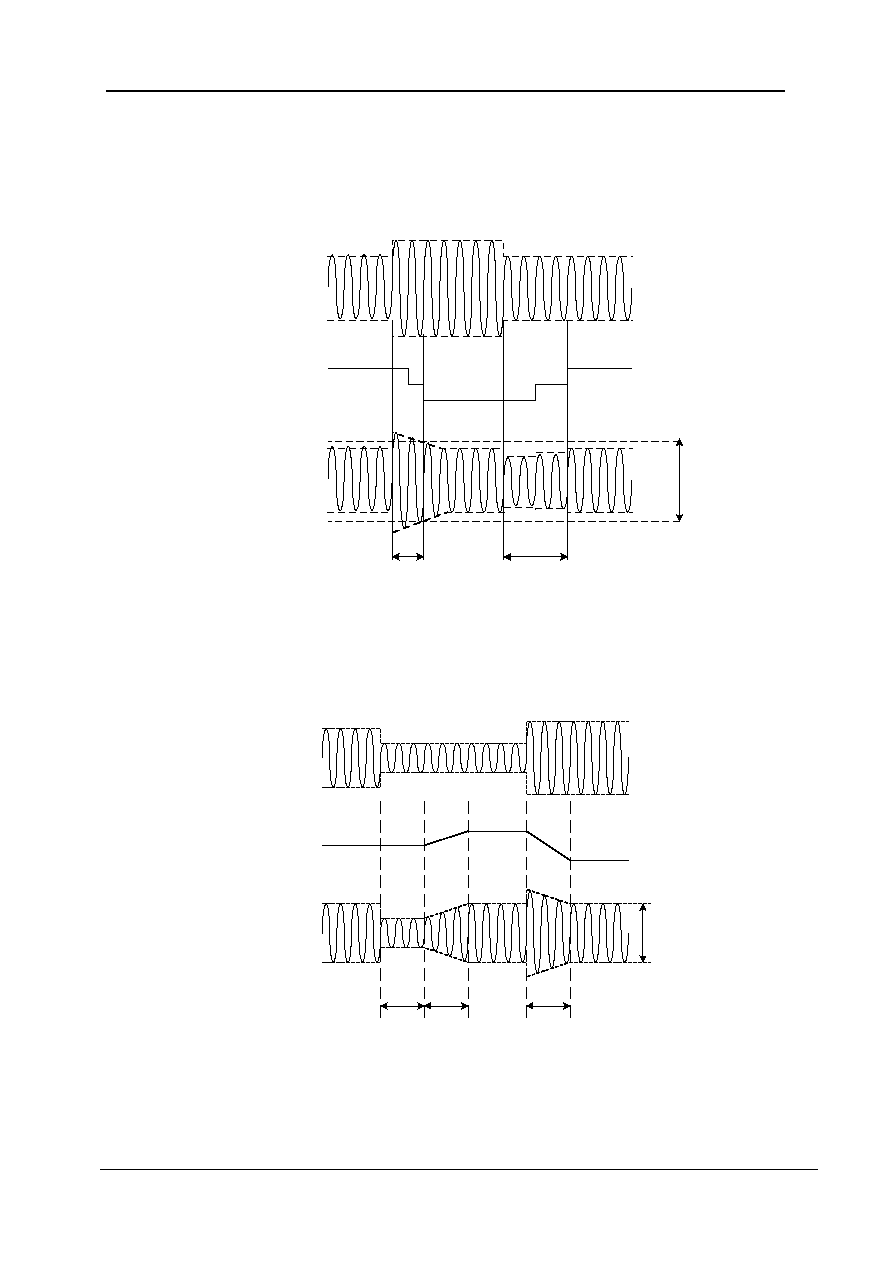
WM8777
Product Preview
w
PP Rev 1.94 November 2004
68
LIMITER / AUTOMATIC LEVEL CONTROL (ALC)
The WM8777 has an automatic PGA gain control circuit, which can function as a peak limiter or as
an automatic level control (ALC). In peak limiter mode, a digital peak detector detects when the input
signal goes above a predefined level and will ramp the PGA gain down to prevent the signal
becoming too large for the input range of the ADC. When the signal returns to a level below the
threshold, the PGA gain is slowly returned to its starting level. The peak limiter cannot increase the
PGA gain above its static level.
Figure 30 Limiter Operation
In ALC mode, the circuit aims to keep a constant recording volume irrespective of the input signal
level. This is achieved by continuously adjusting the PGA gain so that the signal level at the ADC
input remains constant. A digital peak detector monitors the ADC output and changes the PGA gain
if necessary.
Figure 31 ALC Operation
hold
time
decay
time
attack
time
input
signal
signal
after
ALC
PGA
gain
ALC
target
level
input
signal
signal
after
PGA
PGA
gain
Limiter
threshold
attack
time
decay
time

Product Preview
WM8777
w
PP Rev 1.94 November 2004
69
The gain control circuit is enabled by setting the LCEN control bit. The user can select between
Limiter mode and three different ALC modes using the LCSEL control bits.
REGISTER
ADDRESS
BIT LABEL DEFAULT
DESCRIPTION
(1Eh)
ALC Control 2
8
LCEN
0
Enable the PGA gain control circuit.
0 = PGA gain control disabled
1 = PGA gain control enabled
(1Dh)
ALC Control 1
8:7
LCSEL[1:0]
00
ALC/Limiter function select
00 = Limiter
01 = ALC Right channel only
10 = ALC Left channel only
11 = ALC Stereo
Table 72 ALC Control Registers
The limiter function only operates in stereo, which means that the peak detector takes the maximum
of left and right channel peak values, and any new gain setting is applied to both left and right PGAs,
so that the stereo image is preserved. However, the ALC function can also be enabled on one
channel only. In this case, only one PGA is controlled by the ALC mechanism, while the other
channel runs independently with its PGA gain set through the control register.
When enabled, the threshold for the limiter or target level for the ALC is programmed using the LCT
control bits. This allows the threshold/target level to be programmed between -1dB and -16dB in 1dB
steps. Note that for the ALC, target levels of -1dB and -2dB give a threshold of -3dB. This is because
the ALC can give erroneous operation if the target level is set too high.
REGISTER
ADDRESS
BIT LABEL DEFAULT
DESCRIPTION
(1Dh)
ALC Control 1
3:0 LCT[3:0] 1011
(-6dB)
Limiter Threshold/ALC target level in
1dB steps.
0000 = -16dB FS
0001 = -15dB FS
...
1101 = -3dB FS
1110 = -2dB FS
1111 = -1dB FS
Table 73 Limiter Threshold Register
ATTACK AND DECAY TIMES
The limiter and ALC have different attack and decay times which determine their operation. However,
the attack and decay times are defined slightly differently for the limiter and for the ALC. DCY and
ATK control the decay and attack times, respectively.
Decay time (Gain Ramp-Up). When in ALC mode, this is defined as the time that it takes for the
PGA gain to ramp up across 90% of its range (e.g. from ≠21dB up to +20 dB). When in limiter mode,
it is defined as the time it takes for the gain to ramp up by 6dB.
The decay time can be programmed in power-of-two (2
n
) steps. For the ALC this gives times from
33.6ms, 67.2ms, 134.4ms etc. to 34.41s. For the limiter this gives times from 1.2ms, 2.4ms etc., up
to 1.2288s. However, the decay time for the limiter can also be made dependant on the input
frequency by setting the FDECAY control bit. For a 1kHz input signal this gives decay times of 24ms,
48ms etc., up to 24.576s.
Attack time (Gain Ramp-Down) When in ALC mode, this is defined as the time that it takes for the
PGA gain to ramp down across 90% of its range (e.g. from +20dB down to -21dB gain). When in
limiter mode, it is defined as the time it takes for the gain to ramp down by 6dB.
The attack time can be programmed in power-of-two (2
n
) steps, from 8.4ms, 16.8ms, 33.6ms etc. to
8.6s for the ALC and from 250us, 500us, etc. up to 256ms.
The time it takes for the recording level to return to its target value or static gain value therefore
depends on both the attack/decay time and on the gain adjustment required. If the gain adjustment is
small, it will be shorter than the attack/decay time.

WM8777
Product Preview
w
PP Rev 1.94 November 2004
70
REGISTER
ADDRESS
BIT LABEL DEFAULT
DESCRIPTION
LC attack (gain ramp-down) time
3:0 ATK[3:0] 0010
ALC mode
0000 = 8.4ms
0001 = 16.8ms
0010 = 33.6ms...
(time doubles with
every step)
1010 or higher =
8.6s
Limiter Mode
0000 = 250us
0001 = 500us... 0010
= 1ms
(time doubles with
every step)
1010 or higher =
256ms
LC decay (gain ramp-up) time
7:4
DCY[3:0]
0011
ALC mode
0000 = 33.5ms
0001 = 67.2ms
0010 = 134.4ms
....(time doubles for
every step)
1010 or higher =
34.41ms
Limiter mode
0000 = 1.2ms
0001 = 2.4ms
0010 = 4.8ms
....(time doubles for
every step)
1010 or higher =
1.2288s
Frequency dependant decay (limiter only)
0 = Frequency dependent delay disabled
1 = Frequency dependent delay enabled
DCY
20kHz input (or
disabled)
1kHz input
(1Fh)
ALC Control 3
8
FDECAY
0
0000
0001
0010
......
1010 or
higher
1.2ms
2.4ms
4.8ms
......
1.2288ms
24ms
28ms
96ms
......
24.576s
Table 74 ALC Attack and Decay Registers
TRANSIENT WINDOW (LIMITER ONLY)
To prevent the limiter responding to short duration high amplitude signals (such as hand-claps in a
live performance), the limiter has a programmable transient window preventing it responding to
signals above the threshold until their duration exceeds the window period. The Transient window is
set in register TRANWIN.
REGISTER
ADDRESS
BIT LABEL DEFAULT
DESCRIPTION
(21h)
Limiter Control
6:4 TRANWIN
[2:0]
010
Length of Transient Window
000 = 0us (disabled)
001 = 62.5us
010 = 125us
.....
111 = 4ms
Table 75 Transient Window Register
ZERO CROSS
The PGA has a zero cross detector to prevent gain changes introducing noise to the signal. In ALC
mode the register bit ALCZC allows this to be turned on if desired.
REGISTER
ADDRESS
BIT LABEL DEFAULT
DESCRIPTION
(1Eh)
ALC Control 2
7 ALCZC
0
(disabled)
ALC zero cross detection circuit.
0 = Zero cross detection disabled.
1 = Zero cross detection enabled.
Table 76 ALC Zero Cross Register
When the limiter is enabled the zero cross detector on the PGA is automatically enabled to ensure
that no noise is introduced during gain changes.

Product Preview
WM8777
w
PP Rev 1.94 November 2004
71
MAXIMUM GAIN (ALC ONLY) AND MAXIMUM ATTENUATION
To prevent low level signals being amplified too much by the ALC, the MAXGAIN register sets the
upper limit for the gain. This prevents low level noise being over-amplified. The MAXGAIN register
has no effect on the limiter operation.
The MAXATTEN register has different operation for the limiter and for the ALC. For the limiter it
defines the maximum attenuation below the static (user programmed) gain. For the ALC, it defines
the lower limit for the gain.
REGISTER
ADDRESS
BIT LABEL DEFAULT
DESCRIPTION
(1Dh)
ALC Control 1
6:4 MAXGAIN[2:0]
111
(+24dB)
Set maximum gain for the PGA (ALC
only)
111 = +24dB
110 = +20dB
.....(-4dB steps)
010 = +4dB
001 = 0dB
000 = 0dB
Maximum attenuation of PGA
(21h)
Limiter Control
3:0 MAXATTEN
[3:0]
0110
Limiter
(attenuation
below static)
0000 = -3dB
0001 = -4dB
0010 = -5dB
.... (-1dB steps)
1001 = -12dB
ALC (lower PGA
gain limit)
1010 or lower
= -1dB
1011 = -5dB
..... (-4dB steps)
1110 = -17dB
1111 = -21dB
Table 77 ALC MAXGAIN and MAXATTEN Registers
HOLD TIME (ALC ONLY)
The ALC also has a hold time, which is the time delay between the peak level detected being below
target and the PGA gain beginning to ramp up. It can be programmed in power-of-two (2
n
) steps, e.g.
2.67ms, 5.33ms, 10.67ms etc. up to 43.7ms. Alternatively, the hold time can also be set to zero. The
hold time only applies to gain ramp-up, there is no delay before ramping the gain down when the
signal level is above target.
REGISTER
ADDRESS
BIT LABEL DEFAULT
DESCRIPTION
(1Eh)
ALC Control 2
3:0
HLD[3:0]
0000
ALC hold time before gain is
increased.
0000 = 0ms
0001 = 2.67ms
0010 = 5.33ms
... (time doubles with every step)
1111 = 43.691s
Table 78 ALC Hold Time Register
OVERLOAD DETECTOR (ALC ONLY)
To prevent clipping when a large signal occurs just after a period of quiet, the ALC circuit includes an
overload detector. If the ADC input signal exceeds 87.5% of full scale (≠1.16dB), the PGA gain is
ramped down at the maximum attack rate (as when ATK = 0000), until the signal level falls below
87.5% of full scale. This function is automatically enabled whenever the ALC is enabled.
(Note: If ATK = 0000, then the overload detector makes no difference to the operation of the ALC. It
is designed to prevent clipping when long attack times are used).

WM8777
Product Preview
w
PP Rev 1.94 November 2004
72
NOISE GATE (ALC ONLY)
When the signal is very quiet and consists mainly of noise, the ALC function may cause "noise
pumping", i.e. loud hissing noise during silence periods. The WM8777 has a noise gate function that
prevents noise pumping by comparing the signal level at the AINL1/2/3/4/5 and/or AINR1/2/3/4/5 pins
against a noise gate threshold, NGTH. The noise gate cuts in when:
∑
Signal level at ADC [dB] < NGTH [dB] + PGA gain [dB] + Mic Boost gain [dB]
This is equivalent to:
∑
Signal level at input pin [dB] < NGTH [dB]
When the noise gate is triggered, the PGA gain is held constant (preventing it from ramping up as it
would normally when the signal is quiet).
The table below summarises the noise gate control register. The NGTH control bits set the noise
gate threshold with respect to the ADC full-scale range. The threshold is adjusted in 6dB steps.
Levels at the extremes of the range may cause inappropriate operation, so care should be taken with
set≠up of the function. Note that the noise gate only works in conjunction with the ALC function, and
always operates on the same channel(s) as the ALC (left, right, both, or none).
REGISTER
ADDRESS
BIT LABEL DEFAULT
DESCRIPTION
0
NGAT
0
Noise gate function enable
0 = Noise gate disabled
1 = Noise gate enabled
(20h)
Noise Gate
Control
4:2
NGTH[2:0]
000
Noise gate threshold (with respect to
ADC output level)
000 = -78dBFS
001 = -72dBfs
... 6 dB steps
110 = -42dBFS
111 = -30dBFS
Table 79 Noise Gate Registers
Note: The Noise Gate should be set after the ALC to ensure correct operation.
SOFTWARE REGISTER RESET
Writing to register 1111111 will cause a register reset, resetting all register bits to their default
values. Note that the WM8777 is powered down by default so writing to this register will power down
the device.
Table 80 Software Reset Register
REGISTER
ADDRESS
BIT LABEL DEFAULT
DESCRIPTION
(7Fh)
Software reset
8:0
RESET
Writing to this register will apply a
reset to the device registers.

Product Preview
WM8777
w
PP Rev 1.94 November 2004
73
REGISTER MAP
The complete register map is shown below. The detailed description can be found in the relevant text of the device description. The
WM8777 can be configured using the Control Interface. All unused bits should be set to `0'.
REGISTER B15 B14 B13 B12 B11 B10 B9 B8
B7
B6
B5
B4
B3
B2
B1
B0
DEFAULT
R0(00h) 0 0 0 0 0 0 0 UPDATE
FRONTLZCEN
FRONTLA[6:0]
X01101011
R1(01h) 0 0 0 0 0 0 1 UPDATE
FRONTRZCEN
FRONTRA[6:0] X01101011
R2(02h) 0 0 0 0 0 1 0 UPDATE
CNTRZCEN
CNTRA[6:0] X01101011
R3(03h) 0 0 0 0 0 1 1 UPDATE
LFEZCEN
LFEA[6:0] X01101011
R4(04h) 0 0 0 0 1 0 0 UPDATE
SURLZCEN
SURLA[6:0] X01101011
R5(05h) 0 0 0 0 1 0 1 UPDATE
SURLZCEN
SURRA[6:0] X01101011
R6(06h) 0 0 0 0 1 1 0 UPDATE
AUXLZCEN
AUXLA[6:0] X01101011
R7(07h) 0 0 0 0 1 1 1 UPDATE
AUXRZCEN
AUXRA[6:0] X01101011
R8(08h) 0 0 0 1 0 0 0 UPDATE
HPLZCEN
HPLA[6:0] X01101011
R9(09h) 0 0 0 1 0 0 1 UPDATE
HPRZCEN
HPRA[6:0] X01101011
R10(0Ah)
0 0 0 1 0 1 0 UPDATE MZCEN
MASTA[6:0]
X01101011
R11(0Bh)
0 0 0 1 0 1 1 UPDATE LDA1[7:0] X11111111
R12(0Ch) 0 0 0 1 1 0 0 UPDATE RDA1[7:0] X11111111
R13(0Dh) 0 0 0 1 1 0 1 UPDATE LDA2[7:0] X11111111
R14(0Eh)
0 0 0 1 1 1 0 UPDATE RDA2[7:0] X11111111
R15(0Fh)
0 0 0 1 1 1 1 UPDATE LDA3[7:0] X11111111
R16(10h)
0 0 1 0 0 0 0 UPDATE RDA3[7:0] X11111111
R17(11h)
0 0 1 0 0 0 1 UPDATE LDA4[7:0] X11111111
R18(12h)
0 0 1 0 0 1 0 UPDATE RDA4[7:0] X11111111
R19(13h)
0 0 1 0 0 1 1 UPDATE MASTDA[7:0] X11111111
R20(14h)
0 0 1 0 1 0 0
0 PHASE[7:0]
000000000
R21(15h)
0 0 1 0 1 0 1
PL[3:0] TOCDAC
0
IZD
DACATC
DZCEN
100100000
R22(16h)
0 0 1 0 1 1 0
RECREN[1:0]
RECLEN[1:0]
MUTEALL
DMUTE[3:0] 000000000
R23(17h)
0 0 1 0 1 1 1
0 DZFM[3:0]
DEEMP[3:0]
000000000
R24(18h)
0 0 1 1 0 0 0
0
MLCKOUT
SRC
MCLKOPEN
PAIFRX_WL[1:0]
PAIFRX
BCP
PAIFRX
LRP
PAIFRX_FMT[1:0] 000100010
R25(19h)
0 0 1 1 0 0 1 PAIFRX
MS
PAIFTX_MS PAIFRX_RATE[2:0]
DACOSR
PAIFTX_RATE[2:0] 000100010
R26(1Ah)
0 0 1 1 0 1 0 OSCPD
SPDIFRXD SPDIFTXD
DACPD[3:0] ADCPD
PWDN
111111110
R27(1Bh)
0 0 1 1 0 1 1 SYNC ADCOSR ADCHPD
PAIFTX_WL
[1:0]
PAIFTX
BCP
PAIFTX
LRP
PAIFTX_FMT[1:0] 000100010
R28(1Ch) 0 0 1 1 1 0 0
Reserved
000000000
R29(1Dh) 0 0 1 1 1 0 1
LCSEL[1:0] MAXGAIN[2:0]
LCT[3:0]
001111011
R30(1Eh)
0 0 1 1 1 1 0 LCEN ALCZC
0
0
0
HLD[3:0]
000000000
R31(1Fh)
0 0 1 1 1 1 1 FDECAY DCY[3:0]
ATK[3:0]
100110010
R32(20h)
0 1 0 0 0 0 0
0 0 0 0
NGTH[2:0]
0
NGAT
000000000
R33(21h)
0 1 0 0 0 0 1
0 0
TRANWIN[2:0]
MAXATTEN[3:0]
010100110
R34(22h)
0 1 0 0 0 1 0
0 0 AIN6
FBYP
FBM
FBASS[1:0] FTRBL[1:0]
000000000
R35(23h)
0 1 0 0 0 1 1
0 CNTR
CNTRGAIIN[2:0]
FLFE
FLFEGAIN[2:0]
000000000
WM8777
Product Preview
w
PP Rev 1.94 November 2004
74
REGISTER B15 B14 B13 B12 B11 B10 B9 B8
B7
B6
B5
B4
B3
B2
B1
B0
DEFAULT
R36(24h)
0 1 0 0 1 0 0
0 0 0 0 0
REAR REARGAIN[2:0] 000000000
R37(25h)
0 1 0 0 1 0 1
0 0
HPSEL
CBYP
CBM
CBASS[1:0] CTRBL[1:0]
000000000
R38(26h)
0 1 0 0 1 1 0
0 0 0 0 0
CLFE CLFEGAIN[2:0] 000000000
R39(27h)
0 1 0 0 1 1 1
0 0 0 0
0
SURRBYP SURLBYP AUXRBYP AUXLBYP
000000000
R40(28h)
0 1 0 1 0 0 0 UPDATE 0
0
0
0
FBASS[3:0]
000000000
R41(29h)
0 1 0 1 0 0 1 UPDATE 0
0
0
0
FTREB[3:0]
000000000
R42(2Ah)
0 1 0 1 0 1 0 UPDATE 0
0
0
0
CBASS[3:0]
000000000
R43(2Bh)
0 1 0 1 0 1 1 UPDATE 0
0
0
0
CTREB[3:0]
000000000
R44(2Ch)
0 1 0 1 1 0 0 UPDATEL UPDATER UPDATEC
FTLP[1:0] FTRP[1:0] CNTP[1:0]
000000000
R45(2Dh)
0 1 0 1 1 0 1 HPPD FTRPD FTLPD CTRPD
LFEPD
SURRPD
SURLPD
AUXRPD
AUXLPD
111111111
R46(2Eh)
0 1 0 1 1 1 0 ZCLEN
LAG[7:0] 011001111
R47(2Fh)
0 1 0 1 1 1 1 ZCREN
RAG[7:0]
011001111
R48(30h)
0 1 1 0 0 0 0
0 0 0 0
0
TOADC
ADC
ATC
MUTER MUTEL 000000000
R49(31h)
0 1 1 0 0 0 1 AINPD 0
0
AIN[5:0]
100000000
R50(32h)
0 1 1 0 0 1 0 OUTPD2 OUTPD1
0
MX2[2:0]
MX1[2:0]
110001001
R51(33h)
0 1 1 0 0 1 1 OUTPD4 OUTPD3
0
0
MX4[1:0]
MX3[2:0]
110001001
R52(34h)
0 1 1 0 1 0 0
PLL_K[8:0] 100100001
R53(35h)
0 1 1 0 1 0 1
PLL_K[17:9] 101111110
R54(36h)
0 1 1 0 1 1 0 PLL2TX
PLL2
ADC
PLL2
DAC
0
CLKOUTS
RC
PLL_K[21:18] 100001101
R55(37h)
0 1 1 0 1 1 1
PLL_N[4:0]
PRESCALE FRAC_E
N
POSTSCA
LE
PLLPD 000000011
R56(38h)
0 1 1 1 0 0 0
0 DAC4SEL[1:0]
DAC3SEL[1:0]
DAC2SEL[1:0] DAC1SEL[1:0] 011100100
R57(39h)
0 1 1 1 0 0 1
0
CHSTMODE[2:0]
PREEMPH[2:0] CPY_N
AUDIO_N
CON/PRO
000000000
R58(3Ah)
0 1 1 1 0 1 0
0 CATCODE[7:0]
000000000
R59(3Bh)
0 1 1 1 0 1 1
0 CHNUM2[1:0] CHNUM1[1:0]
SRCNUM[3:0]
000000000
R60(3Ch)
0 1 1 1 1 0 0
0 0 0 CLKACU[1:0]
FREQ[3:0]
000110001
R61(3Dh)
0 1 1 1 1 0 1
0 ORGSAMP[3:0] TXPAIFRX_WL[1:0]
MAXPAIFR
X WL
000001011
R62(3Eh)
0 1 1 1 1 1 0
0 0
SAIF_WL
[1:0]
SAIF_B
CP
SAIF_L
RP
SAIF_FMT
[1:0]
000100010
R63(3Fh)
0 1 1 1 1 1 1
0 0 0
SAIFCLKSRC[1:0]
SMS
SAIFRATE[2:0] 000000010
R64(40h)
1 0 0 0 0 0 0
ADCCL
KSRC
ALWAYSVA
LID
FILLMODE RXINSEL[1:0]
0
0
0
SPDINMODE
000000000
R65(41h)
1 0 0 0 0 0 1
0 SAIFSRC[1:0] PAIFSRC[1:0]
TXRXT
HRU
TXSRC[1:0] RX2DAC
000010000
R66(42h)
1 0 0 0 0 1 0
0 0 0
FPLL[2:0]
0
0 0
000111000
R67(43h)
1 0 0 0 0 1 1
Reserved 00000000
R68(44h)
1 0 0 0 1 0 0
Reserved 000000000
R69(45h)
1 0 0 0 1 0 1
Reserved 000000000
R70(46h)
1 0 0 0 1 1 0
Reserved 000000000
R71(47h)
1 0 0 0 1 1 1
0
GPIO2OP[3:0]
GPIO1OP[3:0] 000010000
R72(48h)
1 0 0 1 0 0 0
0
GPOMODEOP[3:0] GPIO3OP[3:0]
010100010
R73(49h)
1 0 0 1 0 0 1
0 MASK[7:0]
000000000

Product Preview
WM8777
w
PP Rev 1.94 November 2004
75
REGISTER B15 B14 B13 B12 B11 B10 B9 B8
B7
B6
B5
B4
B3
B2
B1
B0
DEFAULT
R74(4Ah)
1 0 0 1 0 1 0
0 0 0
READEN2
READEN
3
0 0 0 0
000000000
R75(4Bh)
1 0 0 1 0 1 1
0
SPDIF_MO
DE
CPY_N PCM_N
AUDIO_N
BIP
PARITYERR
VALIDITY
UNLOCK
R76(4Ch)
1 0 0 1 1 0 0
Read Only 1
R77(4Dh)
1 0 0 1 1 0 1
Read Only 2
R78(4Eh)
1 0 0 1 1 1 0
Read Only 3
R79(4Fh)
1 0 0 1 1 1 1
Read Only 4
R80(50h)
1 0 1 0 0 0 0
Read Only 5
R81(51h)
1 0 1 0 0 0 1
Read Only 6
R127(7Fh) 1 1 1 1 1 1 1
RESET See
Notes
ADDRESS
DATA DEFAULT
Table 81 Register Map
Note: Any write to R127 causes a software reset.

WM8777
Product Preview
w
PP Rev 1.94 November 2004
76
REGISTER
ADDRESS
BIT LABEL DEFAULT
DESCRIPTION
6:0
FRONTLA[6:0] 1101011
(0dB)
Analogue Attenuation control for FRONTL in 1dB steps. See
Table 60.
7
FRONTLZCEN 0 FRONTL zero cross detect enable
0 = zero cross disabled
1 = zero cross enabled
0000000
(00h)
Analogue
Attenuation
FRONTL
8
UPDATE Not
latched
Controls simultaneous update of all Analogue Attenuation Latches
0 = Store FRONTL in intermediate latch (no change to
output)
1 = Store FRONTL and update attenuation on all channels.
6:0
FRONTRA[6:0] 1101011
(0dB)
Analogue Attenuation control for FRONTR in 1dB steps. See
Table 60.
7
FRONTRZCEN 0 FRONTR zero cross detect enable
0 = zero cross disabled
1 = zero cross enabled
0000001
(01h)
Analogue
Attenuation
FRONTR
8
UPDATE Not
latched
Controls simultaneous update of all Analogue Attenuation Latches
0 = Store FRONTR in intermediate latch (no change to
output)
1 = Store FRONTR and update attenuation on all channels.
6:0
CNTRA[6:0] 1101011
(0dB)
Analogue Attenuation control for CNTR in 1dB steps. See Table
60.
7
CNTRZCEN 0
CNTR zero cross detect enable
0 = zero cross disabled
1 = zero cross enabled
0000010
(02h)
Analogue
Attenuation
CNTR
8
UPDATE
Not latched
Controls simultaneous update of all Analogue Attenuation Latches
0 = Store CNTR in intermediate latch (no change to output)
1 = Store CNTR and update attenuation on all channels.
6:0
LFEA[6:0]
1101011
(0dB)
Analogue Attenuation control for LFE in 1dB steps. See Table 60.
7
LFEZCEN 0
LFE zero cross detect enable
0 = zero cross disabled
1 = zero cross enabled
0000011
(03h)
Analogue
Attenuation
LFE
8
UPDATE
Not latched
Controls simultaneous update of all Analogue Attenuation Latches
0 = Store LFE in intermediate latch (no change to output)
1 = Store LFE and update attenuation on all channels.
6:0 SURLA[6:0] 1101011
(0dB)
Analogue Attenuation control for SURL in 1dB steps. See Table
60.
7
SURLZCEN 0
SURL zero cross detect enable
0 = zero cross disabled
1 = zero cross enabled
0000100
(04h)
Analogue
Attenuation
SURL
8
UPDATE
Not latched
Controls simultaneous update of all Analogue Attenuation Latches
0 = Store SURL in intermediate latch (no change to output)
1 = Store SURL and update attenuation on all channels.
6:0 SURRA[6:0] 1101011
(0dB)
Analogue Attenuation control for SUR Right in 1dB steps. Table
60.
7
SURRZCEN 0
SURR zero cross detect enable
0 = zero cross disabled
1 = zero cross enabled
0000101
(05h)
Analogue
Attenuation
SURR
8
UPDATE
Not latched
Controls simultaneous update of all Analogue Attenuation Latches
0 = Store SURR in intermediate latch (no change to output)
1 = Store SURR and update attenuation on all channels.

Product Preview
WM8777
w
PP Rev 1.94 November 2004
77
REGISTER
ADDRESS
BIT LABEL DEFAULT
DESCRIPTION
6:0
AUXLA[6:0] 1101011
(0dB)
Analogue Attenuation control for AUXL in 1dB steps. See Table
60.
7
AUXLZCEN 0
AUXL zero cross detect enable
0 = zero cross disabled
1 = zero cross enabled
0000110
(06h)
Analogue
Attenuation
AUXL
8
UPDATE Not
latched
Controls simultaneous update of all Analogue Attenuation Latches
0 = Store AUXL in intermediate latch (no change to output)
1 = Store AUXL and update attenuation on all channels.
6:0
AUXRA[6:0] 1101011
(0dB)
Analogue Attenuation control for AUXR in 1dB steps. See Table
60.
7
AUXRZCEN 0
AUXR zero cross detect enable
0 = zero cross disabled
1 = zero cross enabled
0000111
(07h)
Analogue
Attenuation
AUXR
8
UPDATE Not
latched
Controls simultaneous update of all Analogue Attenuation Latches
0 = Store AUXR in intermediate latch (no change to output)
1 = Store AUXR and update attenuation on all channels.
6:0
HPLA[6:0] 1101011
(0dB)
Analogue Attenuation control for HPHONEL in 1dB steps. See
Table 60.
7
HPLZCEN 0
HPHONEL zero cross detect enable
0 = zero cross disabled
1 = zero cross enabled
0001000
(08h)
Analogue
Attenuation
HPHONEL
8
UPDATE Not
latched
Controls simultaneous update of all Analogue Attenuation Latches
0 = Store HPHONEL in intermediate latch (no change to output)
1 = Store HPHONEL and update attenuation on all channels.
6:0
HPRA[6:0] 1101011
(0dB)
Analogue Attenuation control for HPHONER in 1dB steps. See
Table 60.
7
HPRZCEN 0
HPHONER zero cross detect enable
0 = zero cross disabled
1 = zero cross enabled
0001001
(09h)
Analogue
Attenuation
HPHONER
8
UPDATE Not
latched
Controls simultaneous update of all Analogue Attenuation Latches
0 = Store HPHONER in intermediate latch (no change to output)
1 = Store HPHONER and update attenuation on all channels.
6:0
MASTA[6:0] 1101011
(0dB)
Analogue Attenuation control for all DAC gains in 1dB steps. See
Table 60.
7
MZCEN 0
Master zero cross detect enable
0 = zero cross disabled
1 = zero cross enabled
0001010
(0Ah)
Analogue
Attenuation
Master
(all channels)
8
UPDATE Not
latched
Controls simultaneous update of all Analogue Attenuation Latches
0 = Store gains in intermediate latch (no change to output)
1 = Store gains and update attenuation on all channels.
7:0
LDA1[7:0] 11111111
(0dB)
Digital Attenuation control for DAC1 Left Channel (LSUMOP) in
0.5dB steps. See Table 63
0001011
(0Bh)
Digital
Attenuation
DACL1
8
UPDATE Not
latched
Controls simultaneous update of all Attenuation Latches
0 = Store LDA1 in intermediate latch (no change to output)
1 = Store LDA1 and update attenuation on all channels
7:0
RDA1[6:0] 11111111
(0dB)
Digital Attenuation control for DAC1 Right Channel (RSUMOP) in
0.5dB steps. See Table 63
0001100
(0Ch)
Digital
Attenuation
DACR1
8
UPDATE Not
latched
Controls simultaneous update of all Attenuation Latches
0 = Store RDA1 in intermediate latch (no change to output)
1 = Store RDA1 and update attenuation on all channels.
7:0
LDA2[7:0] 11111111
(0dB)
Digital Attenuation control for DAC2 Left Channel (CNTSOP) in
0.5dB steps. See Table 63
0001101
(0Dh)
Digital
Attenuation
DACL2
8
UPDATE Not
latched
Controls simultaneous update of all Attenuation Latches
0 = Store LDA2 in intermediate latch (no change to output)
1 = Store LDA2 and update attenuation on all channels.

WM8777
Product Preview
w
PP Rev 1.94 November 2004
78
REGISTER
ADDRESS
BIT LABEL DEFAULT
DESCRIPTION
7:0
RDA2[7:0] 11111111
(0dB)
Digital Attenuation control for DAC2 Right Channel (LFESOP) in
0.5dB steps. See Table 63
0001110
(0Eh)
Digital
Attenuation
DACR2
8
UPDATE Not
latched
Controls simultaneous update of all Attenuation Latches
0 = Store RDA2 in intermediate latch (no change to output)
1 = Store RDA2 and update attenuation on all channels.
7:0
LDA3[7:0] 11111111
(0dB)
Digital Attenuation control for DAC3 Left Channel (LSURSOP) in
0.5dB steps. See Table 63
0001111
(0Fh)
Digital
Attenuation
DACL3
8
UPDATE Not
latched
Controls simultaneous update of all Attenuation Latches
0 = Store LDA3 in intermediate latch (no change to output)
1 = Store LDA3 and update attenuation on all channels.
7:0
RDA3[7:0] 11111111
(0dB)
Digital Attenuation control for DAC3 Right Channel (RSURSOP) in
0.5dB steps. See Table 63
0010000
(10h)
Digital
Attenuation
DACR3
8
UPDATE Not
latched
Controls simultaneous update of all Attenuation Latches
0 = Store RDA3 in intermediate latch (no change to output)
1 = Store RDA3 and update attenuation on all channels.
7:0
LDA4[7:0] 11111111
(0dB)
Digital Attenuation control for DAC4 Left Channel (LAUXSOP) in
0.5dB steps. See Table 63
0010001
(11h)
Digital
Attenuation
DACL4
8
UPDATE Not
latched
Controls simultaneous update of all Attenuation Latches
0 = Store LDA4 in intermediate latch (no change to output)
1 = Store LDA4 and update attenuation on all channels.
7:0
RDA4[7:0] 11111111
(0dB)
Digital Attenuation control for DAC4 Right Channel (RAUXSOP) in
0.5dB steps. See Table 63
0010010
(12h)
Digital
Attenuation
DACR4
8
UPDATE Not
latched
Controls simultaneous update of all Attenuation Latches
0 = Store RDA4 in intermediate latch (no change to output)
1 = Store RDA4 and update attenuation on all channels.
7:0
MASTDA[7:0] 11111111
(0dB)
Digital Attenuation control for all DAC channels in 0.5dB steps.
See Table 63
0010011
(13h)
Digital
Attenuation
Master
(all channels)
8
UPDATE Not
latched
Controls simultaneous update of all Attenuation Latches
0 = Store gain in intermediate latch (no change to output)
1 = Store gain and update attenuation on all channels.
0010100
(14h)
DAC Output
Phase
7:0
PHASE[7:0] 00000000
Controls phase of DAC outputs
PHASE[0] = 1 inverts phase of DAC1L output
PHASE[1] = 1 inverts phase of DAC1R output
PHASE[2] = 1 inverts phase of DAC2L output
PHASE[3] = 1 inverts phase of DAC2R output
PHASE[4] = 1 inverts phase of DAC3L output
PHASE[5] = 1 inverts phase of DAC3R output
PHASE[6] = 1 inverts phase of DAC4L output
PHASE[7] = 1 inverts phase of DAC4R output
0
DZCEN 0
DAC Digital Volume Zero Cross Enable:
0 = Zero Cross detect disabled
1 = Zero Cross detect enabled
1
DACATC 0
Attenuator Control
0 = All DACs use attenuations as programmed.
1 = Right channel DACs use corresponding left DAC
attenuations
2
IZD 0
Infinite zero detection circuit control and automute control
0 = Infinite zero detect automute disabled
1 = Infinite zero detect automute enabled
0010101
(15h)
DAC Attenuation
Control
4 TOCDAC
0
DAC Analogue Zero cross detect timeout disable
0 = Timeout enabled
1 = Timeout disabled

Product Preview
WM8777
w
PP Rev 1.94 November 2004
79
REGISTER
ADDRESS
BIT LABEL DEFAULT
DESCRIPTION
DAC Output Control
PL[3:0] Left
Output
Right
Output
PL[3:0] Left
Output
Right
Output
0000 Mute Mute 1000 Mute Right
0001
Left Mute
1001
Left Right
0010 Right Mute 1010 Right Right
0011
(L+R)/2 Mute
1011
(L+R)/2 Right
0100 Mute Left 1100 Mute (L+R)/2
0101
Left Left 1101
Left (L+R)/2
0110 Right Left 1110 Right (L+R)/2
8:5
PL[3:0] 1001
0111
(L+R)/2 Left
1111
(L+R)/2 (L+R)/2
3:0
DMUTE[3:0] 0000
DAC channel soft mute enables:
DMUTE[0] = 1, enable softmute on DAC1.
DMUTE[1] = 1, enable softmute on DAC2.
DMUTE[2] = 1, enable softmute on DAC3.
DMUTE[3] = 1, enable softmute on DAC4.
4
MUTEALL 0
DAC channel master soft mute. Mutes all DAC channels:
0 = disable softmute on all DACs.
1 = enable softmute on all DACs.
6:5
RECLEN
00
RECL Output Enable
00 = REC output muted
01 = REC output ADCL
10 = REC output DAC1L
0010110
(16h)
Mute Control
8:7
RECREN
00
RECR Output Enable
00 = REC output muted
01 = REC output ADCR
10 = REC output DAC1R
3:0
DEEMP[3:0]
0000
De-emphasis mode select:
DEEMPH[0] = 1, enable De-emphasis on DAC1.
DEEMPH[1] = 1, enable De-emphasis on DAC2.
DEEMPH[2] = 1, enable De-emphasis on DAC3.
DEEMPH[3] = 1, enable De-emphasis on DAC4.
0010111
(17h)
DAC Control
7:4
DZFM[3:0] 0000
Selects the ouput for ZFLG1 and ZFLG2 pins (see Table 53).
1 = indicates 1024 consecutive zero input samples on the
channels selected
0 = indicates at least one of selected channels has non
zero sample in last 1024 inputs
1:0 PAIFRX_FMT
[1:0]
10
Interface format select
00 = right justified mode
01 = left justified mode
10 = I
2
S mode
11 = DSP (early or late) mode
PDATAIPLRC Polarity or DSP Early/Late mode select
2 PAIFRX_LRP
0
Left Justified / Right Justified /
I
2
S
0 =Standard PDATAIPLRC
Polarity
1 =Inverted PDATAIPLRC
Polarity
DSP Mode
0 = Early DSP mode
1 = Late DSP mode
0011000
(18h)
Primary
Interface
Control (RX)
3 PAIFRX_BCP
0 PBCLK
Polarity
0 = Normal - DIN[3:0], PDATAIPLRC and PDATAOPLRC
sampled on rising edge of PBCLK; PDATAOP changes on
falling edge of PBCLK.
1 = Inverted - DIN[3:0], PDATAIPLRC and PDATAOPLRC
sampled on falling edge of PBCLK; PDATAOP changes on
rising edge of PBCLK.

WM8777
Product Preview
w
PP Rev 1.94 November 2004
80
REGISTER
ADDRESS
BIT LABEL DEFAULT
DESCRIPTION
5:4 PAIFRX_WL
[1:0]
10
Input Word Length
00 = 16-bit Mode
01 = 20-bit Mode
10 = 24-bit Mode
11 = 32-bit Mode (not supported in right justified mode)
6
MCLKOPEN
0
MCLK pin output enable
0 = MCLK pin is an input
1 = MCLK pin is an output (see MCLKOUTSRC below)
7
MCLKOUTSRC
0
MCLK pin output source
0 = PLL
1 = Crystal clock output.
2:0 PAIFTX_RATE
[2:0]
010
Master Mode MCLK:PDATAOPLRC ratio select:
000 = 128fs
001 = 192fs
010 = 256fs
011 = 384fs
100 = 512fs
101 = 768fs
110 = 1152fs
3 DACOSR
0 DAC oversample rate select:
0 = 128x oversampling
1 = 64x oversampling
6:4 PAIFRX_RATE
[2:0]
010
Master Mode MCLK:PDATAIPLRC ratio select:
000 = 128fs
001 = 192fs
010 = 256fs
011 = 384fs
100 = 512fs
101 = 768fs
110 = 1152fs
7
PAIFTX_MS
0
Master/Slave Interface mode select. If ADCCLKSRC is set high
then this register control whether the ADC clocks are in master or
slave mode/
0 = Slave Mode ≠ PDATAOPLRC and ADCPBCLK are inputs
1 = Master Mode ≠ PDATAOPLRC and ADCPBCLK are outputs
0011001
(19h)
Master Mode
Control
8
PAIFRX_MS
0
Maser/Slave interface mode select
0 = Slave Mode ≠ PDATAOPLRC, PDATAIPLRC and PBCLK are
inputs
1 = Master Mode ≠ PDATAOPLRC, PDATAIPLRC and PBCLK
are outputs
Note if ADCCLKSRC is set high then this register only controls
PDATAIPLRC and PBCLK.
0
PWDN
0
Chip Powerdown Control (works in tandem with the other
powerdown registers):
0 = All digital circuits running, outputs are active
1 = All digital circuits in power save mode, outputs
muted
1 ADCPD
1
ADC
powerdown:
0 = ADC enabled
1 = ADC disabled
0011010
(1Ah)
Powerdown
Control
5:2
DACPD[3:0]
1111
DAC powerdowns (0 = DAC enabled, 1 = DAC disabled)
DACPD[0] = DAC1
DACPD[1] = DAC2
DACPD[2] = DAC3
DACPD[3] = DAC4

Product Preview
WM8777
w
PP Rev 1.94 November 2004
81
REGISTER
ADDRESS
BIT LABEL DEFAULT
DESCRIPTION
6 SPDIFTXD
1 SPDIF_TX
powerdown
0 = SPDIF_TX enabled
1 = SPDIF_TX disabled
7 SPDIFRXD
1 SPDIF_RX
powerdown
0 = SPDIF_RX enabled
1 = SPDIF_RX disabled
8
OSCPD
1
OSC power down
0 = Oscillator enabled
1 = Oscillator disabled
1:0
PAIFTX_FMT
[1:0]
10
Interface format select
00 = right justified mode
01 = left justified mode
10 = I
2
S mode
11 = DSP (early or late) mode
PDATAOPLRC Polarity or DSP Early/Late mode select
2
PAIFTX_LRP
0
Left Justified / Right Justified /
I
2
S
0 =Standard PDATAOPLRC
Polarity
1 =Inverted PDATAOPLRC
Polarity
DSP Mode
0 = Early DSP mode
1 = Late DSP mode
3
PAIFTX_BCP
0 ADCPBCLK/PBCLK
Polarity
0 = Normal ADCPBCLK/PBCLK.
1 = Inverted ADCPBCLK/PBCLK.
5:4
PAIFTX_WL
[1:0]
10
Input Word Length
00 = 16-bit Mode
01 = 20-bit Mode
10 = 24-bit Mode
11 = 32-bit Mode (not supported in right justified mode)
6
ADCHPD
0
ADC Highpass Filter Disable:
0 = Highpass Filter enabled
1 = Highpass Filter disabled
7 ADCOSR
0 ADC oversample rate select
0 = 128x oversampling
1 = 64x oversapmling
0011011
(1Bh)
Primary
Interface
Control (TX)
8 SYNC
0
Sync ADC and DAC together.
0 = Enable SYNC function
1 = Disable Sync function
3:0 LCT[3:0] 1011
(-6dB)
Limiter threshold/ALC target level in 1dB steps.
0000: -16dB FS
0001: -15dB FS
...
1101: -3dB FS
1110: -2dB FS
1111: -1dB FS
6:4 MAXGAIN[2:0]
111
(+24dB)
Set Maximum Gain of PGA
111 = +24dB
110 = +20dB
....(-4dB steps)
010 = +4dB
001 = 0dB
000 = 0dB
0011101
(1Dh)
ALC Control 1
8:7 LCSEL[1:0]
00
(OFF)
ALC/Limiter function select
00 = Limiter
01 = ALC Right channel only
10 = ALC Left channel only
11 = ALC Stereo (PGA registers unused)

WM8777
Product Preview
w
PP Rev 1.94 November 2004
82
REGISTER
ADDRESS
BIT LABEL DEFAULT
DESCRIPTION
3:0 HLD[3:0] 0000
(0MS)
ALC hold time before gain is increased.
0000 = 0ms
0001 = 2.67ms
0010 = 5.33ms
... (time doubles with every step)
1111 = 43.691s
7
ALCZC
0
ALC zero cross detection circuit.
0 = Zero cross detection disabled.
1 = Zero cross detection enabled.
0011110
(1Eh)
ALC Control 2
8
LCEN
0
Enable the PGA gain control circuit.
0 = PGA gain control disabled
1 = PGA gain control enabled
ALC/Limiter attack (gain ramp down) time
3:0 ATK[3:0]
0010
(33ms/1ms)
ACL mode
0000 = 8.4ms
0001 = 16.8ms
0010 = 33.6ms..
(time doubles with every step)
1010 or higher = 8.6s
Limiter mode
0000 = 250us
0001 = 500us
0010 = 1ms
(time doubles with every step)
1010 or higher = 256ms
ALC/Limiter decay (gain ramp up) time
7:4 DCY[3:0]
0011
ACL mode
0000 = 33.5ms
0001 = 67.2ms
0010 = 134.4ms..
(time doubles with every step)
1010 or higher = 34.41s
Limiter mode
0000 = 1.2ms
0001 = 2.4ms
0010 = 4.8ms
(time doubles with every step)
1010 or higher = 1.2288s
Frequency dependant decay enable (Limiter only)
0 = Frequency dependent decay disabled
1 = Frequency dependent decay enabled
DCY
20KHz input (or disabled)
1KHz input
0011111
(1Fh)
ALC Control 3
8 FDECAY
0
0000
0001
0010
.....
1010 or higher
1.2ms
2.4ms
4.8ms
.....
1.2288s
24ms
48ms
96ms
.....
24.576s
0
NGAT
0
Noise gate enable (ALC only)
0 = Noise gate disabled
1 = Noise gate enabled
0100000
(20h)
Noise Gate
Control
4:2
NGTH[2:0]
000
Noise gate threshold
000 = -78dBFS
001 = -72dBfs
... 6 dB steps
110 = -42dBFS
111 = -36dBFS
Maximum attenuation of PGA
0100001
(21h)
Limiter
Control
3:0 MAXATTEN
[3:0]
0110
ALC
(lower PGA gain limit)
1010 or lower = -1dB
1011 = -5dB
...... (-4dB steps)
1110 = -17dB
1111 = -21dB
Limiter
(attenuation below static)
0000 = -3dB
0001 = -4dB
0010 = -5dB
.... (-1dB steps)
1001 = -12dB

Product Preview
WM8777
w
PP Rev 1.94 November 2004
83
REGISTER
ADDRESS
BIT LABEL DEFAULT
DESCRIPTION
6:4
TRANWIN [2:0]
010
Length of Transient Window
000 = 0us (disabled)
001 = 62.5us
010 = 125us
.....
111 = 4ms
1:0
FTRBL[1:0]
00
Control treble boost and cut:-
00 = both off ( Amps disabled)
01 = Treble cut
10 = Treble boosted
11 = both off (Amps enabled)
3:2
FBASS[1:0]
00
Controls bass boost and cut:-
00 = both off (Amps disabled)
01 = Bass cut
10 = Bass boosted
11 = both off (Amps enabled)
4
FBM
0
Bass managed signal path select
0 = Path disabled
1 = Path enabled
5
FBYP
0
Bypass signal path select
0 = Path disabled
1 = Path enabled
0100010
(22h)
FRONT Mixer
Control 1
6
AIN6
0
0 = AIN6 not selected
1 = AIN6 applied to FRONT channels
2:0
FLFEGAIN[2:0]
000
Front LFE gain:
000 = 0dB
001 = 1dB
010 = 2dB
011 = 3dB
100 = 4dB
101 = 4.5dB
110 = 5dB
111 = 6dB
3
FLFE
0
LFE signal path select
0 = Path disabled
1 = Path enabled
6:4
CNTRGAIN[2:0]
000
Front CNTR gain:
000 = 0dB
001 = 1dB
010 = 2dB
011 = 3dB
100 = 4dB
101 = 4.5dB
110 = 5dB
111 = 6dB
0100011
(23h)
FRONT Mixer
Control 2
7
CNTR
0
Center signal path mix
0 = Path disabled
1 = Path enabled
0100100
(24h)
FRONT Mixer
Control 3
2:0
REARGAIN[2:0]
000
Front REAR gain:
000 = 0dB
001 = 1dB
010 = 2dB
011 = 3dB
100 = 4dB
101 = 4.5dB
110 = 5dB
111 = 6dB

WM8777
Product Preview
w
PP Rev 1.94 November 2004
84
REGISTER
ADDRESS
BIT LABEL DEFAULT
DESCRIPTION
3
REAR
0
Rear signal path mix
0 = Path disabled
1 = Path enabled
1:0
CTRBL[1:0]
00
Control treble boost and cut:
00 = both off (Amps disabled)
01 = Treble cut
10 = Treble boosted
11 = both off (Amps enabled)
3:2
CBASS[1:0]
00
Controls bass boost and cut:-
00 = both off (Amps disabled)
01 = Bass cut
10 = Bass boosted
11 = both off (Amps enabled)
4
CBM
0
Bass managed signal path select
0 = Path disabled
1 = Path enabled
5
CBYP
0
Bypass signal path select
0 = Path disabled
1 = Path enabled
0100101
(25h)
Center Mixer
Control 1
6
HPSEL
0
Controls headphone output MUX:-
0 = FRONTL/R output on headphone channels
1 = AUXL/R output on headphone channels
2:0
CLFEGAIN[2:0]
000
Center LFE gain:
000 = 0dB
001 = 1dB
010 = 2dB
011 = 3dB
100 = 4dB
101 = 4.5dB
110 = 5dB
111 = 6dB
0100110
(26h)
Center Mixer
Control 2
3
CLFE
0
LFE signal path select:
0 = Path disabled
1 = Path enabled
0
AUXLBYP
0
Bypass select for AUX left output
0 = Bass managed
1 = Bypass
1
AUXRBYP
0
Bypass select for AUX right output
0 = Bass managed
1 = Bypass
2
SURLBYP
0
Bypass select for surround left output
0 = Bass managed
1 = Bypass
0100111
(27h)
Bass
Management
Bypass
3
SURRBYP
0
Bypass select for surround right output
0 = Bass managed
1 = Bypass
3:0
FBASS[3:0]
0000
Gain control for Bass boost/cut ≠ see table 3
0101000
(28h)
Front Bass
Control
8
UPDATE Not
latched
Controls simultaneous update of all Attenuation Latches
0 = Store GAIN FRONT BASS in intermediate latch (no
change to output)
1 = Store GAIN FRONT BASS and update attenuation on
all channels.
0101001
3:0
FTREB[3:0]
0000
Gain control for Bass boost/cut ≠ see table 3

Product Preview
WM8777
w
PP Rev 1.94 November 2004
85
REGISTER
ADDRESS
BIT LABEL DEFAULT
DESCRIPTION
(29h)
Front Treble
Control
8
UPDATE Not
latched
Controls simultaneous update of all Attenuation Latches
0 = Store GAIN FRONT TREBLE in intermediate latch (no
change to output)
1 = Store GAIN FRONT TREBLE and update attenuation
on all channels.
3:0
CBASS[3:0]
0000
Gain control for Bass boost/cut ≠ see table 3
0101010
(2Ah)
Center Bass
Control
8
UPDATE Not
latched
Controls simultaneous update of all Attenuation Latches
0 = Store GAIN CENTER BASS in intermediate latch (no
change to output)
1 = Store GAIN CENTER BASS and update attenuation on
all channels.
3:0
CTREB[3:0]
0000
Gain control for Bass boost/cut ≠ see table 3
0101011
(2Bh)
Center Treble
Control
8
UPDATE Not
latched
Controls simultaneous update of all Attenuation Latches
0 = Store GAIN CENTER TREBLE in intermediate latch
(no change to output)
1 = Store GAIN CENTER TREBLE and update attenuation
on all channels.
1:0
CNTP[1:0]
00
PREGAIN control for CNTR control channel
00 = 0dB Attenuation
01 = -6dB Attenuation
10 = -12dB Attenuation
11 = -18dB Attenuation
3:2
FTRP[1:0]
00
PREGAIN control for FRONTR tone control channel
00 = 0dB Attenuation
01 = -6dB Attenuation
10 = -12dB Attenuation
11 = -18dB Attenuation
5:4
FTLP[1:0]
00
PREGAIN control for FRONTL tone control channel
00 = 0dB Attenuation
01 = -6dB Attenuation
10 = -12dB Attenuation
11 = -18dB Attenuation
6
UPDATEC
0
Controls simultaneous update of all Attenuation Latches
0 = Store PREGAIN CNTR in intermediate latch (no
change to output)
1 = Store PREGAIN CNTR and update attenuation on all
channels.
7
UPDATER
0
Controls simultaneous update of all Attenuation Latches
0 = Store PREGAIN RIGHT in intermediate latch (no
change to output)
1 = Store PREGAIN RIGHT and update attenuation on all
channels.
0101100
(2Ch)
Mixer Pregain
8
UPDATEL
0
Controls simultaneous update of all Attenuation Latches
0 = Store PREGAIN LEFT in intermediate latch (no change
to output)
1 = Store PREGAIN LEFT and update attenuation on all
channels.
0
AUXLPD
1
Auxiliary left output powerdown.
0 = powerup
1 = powerdown
1
AUXRPD
1
Auxiliary left output powerdown.
0 = powerup
1 = powerdown
0101101
(2Dh)
Output
Powerdown
2
SURLPD
1
Surround left output powerdown.
0 = powerup
1 = powerdown

WM8777
Product Preview
w
PP Rev 1.94 November 2004
86
REGISTER
ADDRESS
BIT LABEL DEFAULT
DESCRIPTION
3
SURRPD
1
Surround Right output powerdown.
0 = powerup
1 = powerdown
4
LFEPD
1
LFE output powerdown.
0 = powerup
1 = powerdown
5
CTRPD
1
Center output powerdown.
0 = powerup
1 = powerdown
6
FRTLPD
1
Front Left output powerdown.
0 = powerup
1 = powerdown
7
FRTRPD
1
Front Right output powerdown.
0 = powerup
1 = powerdown
8
HPPD
1
Headphone output powerdown.
0 = powerup
1 = powerdown
7:0 LAG[7:0] 11001111
(0dB)
Attenuation control for left channel ADC gain in 0.5dB steps. See
Table 68
0101110
(2Eh)
Attenuation
ADC Left
8
ZCLEN
0
Zero Cross enable for left channel ADC
0 = Disable Zero Cross
1 = Enable Zero Cross
7:0 RAG[7:0] 11001111
(0dB)
Attenuation control for right channel ADC gain in 0.5dB steps.
See Table 68
0101111
(2Fh)
Attenuation
ADC Right
8
ZCREN
0
Zero Cross enable for right channel ADC
0 = Disable Zero Cross
1 = Enable Zero Cross
0
MUTEL
0
Left Channel mute control
0 = Channel not muted
1 = Channel muted
1
MUTER
0
Left Channel mute control
0 = Channel not muted
1 = Channel muted
2 ADCATC
0 Attenuator
Control
0 = ADC use attenuations as programmed.
1 = Right channel ADC use corresponding left ADC attenuations
0110000
(30h)
Attenuation
Control
3
TOADC
0
Time out clock enable/disable
0 = Time out clock enabled.
1 = Time out clock disabled.

Product Preview
WM8777
w
PP Rev 1.94 November 2004
87
REGISTER
ADDRESS
BIT LABEL DEFAULT
DESCRIPTION
5:0
AIN[5:0]
00000
ADC left channel input mux control bits
00000 = UTE
00001 = AIN1
00010 = AIN2
00011 = AIN1 + AIN2
......
11111 = AIN1 + AIN2 + AIN3 + AIN4 + AIN5 + AIN6
0110001
(31h)
ADC Mux and
Powerdown
Control
8
AINPD
1
Input mux and buffer powerdown
0 = Input mux and buffer enabled
1 = Input mux and buffer powered down
2:0
MX1[2:0]
001
VOUT1 Output select (see Figure 28)
5:3
MX2[2:0]
001
VOUT2 Output select (see Figure 28)
7
OUTPD1
1
Mixer Powerdown select
0 = Powerup
1 = Powerdown
0110010
(32h)
Output Mux
and
Powerdown
Control 1
8
OUTPD2
1
Mixer Powerdown select
0 = Powerup
1 = Powerdown
2:0
MX3[2:0]
001
VOUT3 Output select (see Figure 28)
4:3
MX4[1:0]
01
VOUT4 Output select (see Figure 29)
7
OUTPD3
1
Mixer Powerdown select
0 = Powerup
1 = Powerdown
0110011
(33h)
Output Mux
and
Powerdown
Control 2
8
OUTPD4
1
Mixer Powerdown select
0 = Powerup
1 = Powerdown
0110100
(34h)
PLL Control 1
8:0
PLL_K[8:0]
121 (Hex)
Fractional (K) part of PLL input/output frequency ratio (bits 8:0).
0110101
(35h)
PLL Control 2
8:0
PLL_K[17:9]
17E (Hex)
Fractional (K) part of PLL input/output frequency ratio (bits 17:9).
3:0
PLL_K[21:18]
D(Hex)
Fractional (K) part of PLL input/output frequency ratio (bits 21:18)
4
CLKOUTSRC
0
CLKOUT pin source:-
0 = PLL clock output
1 = Crystal clock output.
6
PLL2DAC
0
DAC clock source
0 = MCLK pin
1 = PLL clock
7
PLL2ADC
0
ADC clock source
0 = MCLK or ADCMLCK pin
1 = PLL clock
0110110
(36h)
PLL Control 3
8
PLL2TX
1
S/PDIF TX clock source
0 = MLCK or ADCMCLK pin
1 = PLL clock
0
PLLPD
1
0 = Enable PLL
1 = Disable PLL
1
POSTSCALE
0
0 = no post scale
1= divide MCLK by 2 after PLL
2
FRAC_EN
0
0 = Integer N only PLL
1 = Integer N and Fractional K PLL
3
PRESCALE
0
0 = no pre-scale
1 = divide MCLK by 2 prior to PLL
0110111
(37h)
PLL Control 4
8:4
PLL_N[4:0]
00000
Integer (N) divisor part of PLL input/output frequency ratio. Use
values greater than 5 and less than 13.

WM8777
Product Preview
w
PP Rev 1.94 November 2004
88
REGISTER
ADDRESS
BIT LABEL DEFAULT
DESCRIPTION
1:0 DAC1SEL[1:0]
00
3:2 DAC2SEL[1:0]
01
5:4 DAC3SEL[1:0]
10
0111000
(38h)
DAC Digital
Input Selector
7:6 DAC4SEL[1:0]
11
DAC digital input select.
00 = DAC takes data from PDATAIP1
01 = DAC takes data from PDATAIP2
10 = DAC takes data from PDATAIP3
11 = DAC takes data from PDATAIP4
0
CON/PRO
0
0 = Consumer Mode
1 = Professional Mode (not supported by WM8777)
1
AUDIO_N
0
0 = S/PDIF transmitted data is audio PCM.
1 = S/PDIF transmitted data is not audio PCM.
2
CPY_N
0
0 = Transmitted data has copyright asserted.
1 = Transmitted data has no copyright assertion.
5:3
PREEMPH[2:0]
000
000 = Data from Audio interface has no pre-emphasis.
001 = Data from Audio interface has pre-emphasis.
010 = Reserved (Audio interface has pre-emphasis).
011 = Reserved (Audio interface has pre-emphasis).
All other modes are reserved and should not be used.
0111001
(39h)
S/PDIF
Transmitter
Channel Bit
Control 1
7:6
CHSTMODE[1:0]
00
S/PDIF Channel status bits.
00 = Only valid mode for consumer applications.
All other modes are reserved.
0111010
(3Ah)
S/PDIF
Transmitter
Channel Bit
Control 2
7:0
CATCODE[7:0]
00000000
Category Code. Refer to S/PDIF specification for details.
00h indicates "general" mode.
3:0
SRCNUM[3:0]
0000
Source Number. No definitions are attached to data. See S/PDIF
specification for details.
Channel Number for Subframe 1
CHNUM1
Channel Status Bits[23:20]
00
0000: Do not use channel number
01
0001: Send to Left Channel
10
0010: Send to Right Channel
5:4 CHNUM1[1:0]
00
11
0000: Do not use channel number
Channel Number for Subframe 2
CHNUM2
Channel Status Bits[23:20]
00
0000: Do not use channel number
01
0001: Send to Left Channel
10
0010: Send to Right Channel
0111011
(3Bh)
S/PDIF
Transmitter
Channel Bit
Control 3
7:6 CHNUM2[1:0]
00
11
0000: Do not use channel number
3:0
FREQ[3:0]
0001
Sampling Frequency. See S/PDIF specification for details.
0001 = Sampling Frequency not indicated.
0111100
(3Ch)
S/PDIF
Transmitter
Channel Bit
Control 4
5:4
CLKACU[1:0]
11
Clock Accuracy of Generated clock.
00 = Level II
01 = Level I
10 = Level III
11 = Interface frame rate not matched to sampling frequency.
0111101
(3Dh)
S/PDIF
0
MAXPAIFRX_WL
1
Maximum Audio sample word length
0 = 20 bits
1 = 24 bits

Product Preview
WM8777
w
PP Rev 1.94 November 2004
89
REGISTER
ADDRESS
BIT LABEL DEFAULT
DESCRIPTION
Audio Sample Word Length.
000 = Word Length Not Indicated
TXPAIFRX_WL MAXPAIFRX_WL=
=1
MAXPAIFRX_WL=
=0
001
20 bits
16 bits
010
22 bits
18 bits
100
23 bits
19 bits
101
24 bits
20 bits
110
21 bits
17 bits
3:1 TXPAIFRX_WL
[2:0]
101
All other combinations reserved
7:4
ORGSAMP[3:0]
0000
Original Sampling Frequency. See S/PDIF specification for
details.
0000 = original sampling frequency not indicated
1:0
SAIF_FMT
[1:0]
10
Secondary Audio Interface format select
00 = right justified mode
01 = left justified mode
10 = I
≤
S mode
11 = DSP (early or late) mode
SLRCLK Polarity or DSP Early/Late mode select
2
SAIF_LRP
0
Left Justified / Right Justified/
I
2
S
0 = Standard PDATAIPLRC
Polarity
1 = Inverted PDATAIPLRC
Polarity
DSP Mode
0 = Early DSP mode
1 = Late DSP mode
3
SAIF_BCP
0 SPBCLK
Polarity
0 = Normal SPBCLK.
1 = Inverted SPBCLK.
0111110
(3Eh)
Secondary
Interface
Control
5:4
SAIF_WL
[1:0]
10
Input Word Length
00 = 16-bit Mode
01 = 20-bit Mode
10 = 24-bit Mode
11 = 32-bit Mode (not supported in right justified mode)
2:0
SAIFRATE[2:0]
010
Master Mode MCLK:SLRC ratio select:
000 = 128fs
001 = 192fs
010 = 256fs
011 = 384fs
100 = 512fs
101 = 768fs
110 = 1152fs
3
SMS
0
Maser/Slave interface mode select
0 = Slave Mode ≠ SLRC and SPBCLK are inputs
1 = Master Mode ≠ SLRC and SPBCLK are outputs
0111111
(3Fh)
Secondary
Interface
Master Mode
Control
5:4
SAIFCLKSRC[1:0]
00
Audio interface master clock source when SMS is 1.
00 = MCLK
01 = GPIO (If ADCCLKSRC is set)
10 = PLL clock
11 = PLL clock
1000000
(40h)
S/PDIF
Receiver
0
SPDINMODE
0
Selects the input circuit type for the S/PDIF input
0 = Normal CMOS input
1 = Comparator input. Compatible with 200mV AC coupled
consumer S/PDIF input signals.

WM8777
Product Preview
w
PP Rev 1.94 November 2004
90
REGISTER
ADDRESS
BIT LABEL DEFAULT
DESCRIPTION
5:4 RXINSEL[1:0]
00
S/PDIF Receiver input mux select. Note that the general purpose
inputs must be configured using GPIOxOP to be either CMOS or
comparator inputs if selected by RXINSEL.
00 = S/PDIF_IN1
01 = S/PDIF_IN2 (GPIO1)
10 = S/PDIF_IN3 (GPIO2)
11 = S/PDIF_IN4 (GPIO3)
6 FILLMODE
0
Determines what SPDIF_RX should do if the validity bit indicates
invalid data:
0 = Data from SPDIF_RX remains static at last valid sample.
1 = Data from SPDIF_RX is output as all zeros.
7 ALWAYSVALID
0
Used to override the recovered validity bit.
0 = Use validity bit.
1 = Ignore validity bit.
Input Selector
8 ADCCLKSRC
0
ADC clock source
0 = ADCMCLK is from MCLK pin and ADCPBCLK is from PBCLK
pin
1 = ADCMCLK is from GPIO1, and ADPBCLK is from GPIO2.
(Note that when in this mode RXINSEL must not be set to 01 or
10.)
0
RX2DAC
0
Received S/PDIF PCM data to DAC.
0 = DAC1 takes data from Primary Audio Interface.
1 = DAC1 takes data from S/PDIF receiver.
2:1
TXSRC[1:0]
00
S/PDIF Transmitter Data Source.
00 = S/PDIF received data.
01 = ADC digital output data.
10 = Secondary Audio Interface received data
11 = DAC Audio Interface Received data.
3
TXRXTHRU
0
Only used if TXSRC==00. Configures only the Channel Bit in the
S/PDIF frame.
0 = Channel data equal to recovered channel data.
1 = Channel data taken from channel status registers.
5:4
PAIFSRC[1:0]
01
Audio Interface output source
00 = S/PDIF received data
01 = ADC digital output data
10 = Secondary Audio Interface received data
11 = Power-down Primary Audio Interface Transmitter
1000001
(41h)
Interface
Source Select
7:6
SAIFSRC[1:0]
00
Secondary Audio Interface Transmitter Data Source.
00 = S/PDIF received data.
01 = ADC digital output data.
10 = Power-down Secondary Audio Interface Transmitter
11 = Primary Audio Interface received data.
1000010
(42h)
S/PDIF
Data/Clock
Recovery
5:3
FPLL[2:0]
111
Select jitter attenuation bandwidth.
000 = Invalid
001 = 28.84Hz
010 = 14.92Hz
011 = 7.46Hz
100 = 3.73Hz
101 = 1.87Hz
110 = 0.97Hz
111 = 0.47Hz

Product Preview
WM8777
w
PP Rev 1.94 November 2004
91
REGISTER
ADDRESS
BIT LABEL DEFAULT
DESCRIPTION
3:0
GPIO1OP[3:0]
0000
0000 = INT
0001 = V - Validity
0010 = U - User Data bit
0011 = C - Channel Status Data
0100 = P - Parity bit
0101 = Non-audio (AUDIO_N || PCM_N)
0110 = UNLOCK
0111 = CSUD (Channel Status Registers Updated)
1000 = Zero Flag 1 output
1001 = Zero Flag 2 output
1010 = GPIO1set as S/PDIF input (standard CMOS input buffer)
1011 = GPIO1set as S/PDIF input (`comparator' input for AC
coupled consumer S/PDIF signals)
1100 = Sub Frame clock (1 = sub-frame1, 0 = sub-frame2)
1101 = Start of Block signal
1000111
(47h)
GPIO
Control 1
7:4
GPIO2OP[3:0]
0001
0000 = INT
0001 = V - Validity
0010 = U - User Data bit
0011 = C - Channel Status Data
0100 = P - Parity bit
0101 = Non-audio (AUDIO_N || PCM_N)
0110 = UNLOCK
0111 = CSUD (Channel Status Registers Updated)
1000 = Zero Flag 1 output
1001 = Zero Flag 2 output
1010 = GPIO2set as S/PDIF input (standard CMOS input buffer)
1011 = GPIO2set as S/PDIF input (`comparator' input for AC
coupled consumer S/PDIF signals)
1100 = Sub Frame clock (1 = sub-frame1, 0 = sub-frame2)
1101 = Start of Block signal
1001000
(48h)
GPIO
Control 2
3:0
GPIO3OP[3:0]
0010
0000 = INT
0001 = V - Validity
0010 = U - User Data bit
0011 = C - Channel Status Data
0100 = P - Parity bit
0101 = Non-audio (AUDIO_N || PCM_N)
0110 = UNLOCK
0111 = CSUD (Channel Status Registers Updated)
1000 = Zero Flag 1 output
1001 = Zero Flag 2 output
1010 = GPIO3set as S/PDIF input (standard CMOS input buffer)
1011 = GPIO3set as S/PDIF input (`comparator' input for AC
coupled consumer S/PDIF signals)
1100 = Sub Frame clock (1 = sub-frame1, 0 = sub-frame2)
1101 = Start of Block signal

WM8777
Product Preview
w
PP Rev 1.94 November 2004
92
REGISTER
ADDRESS
BIT LABEL DEFAULT
DESCRIPTION
7:4
GPOMODEOP
[3:0]
1010
0000 = INT
0001 = V - Validity
0010 = U - User Data bit
0011 = C - Channel Status Data
0100 = P - Parity bit
0101 = Non-audio (AUDIO_N || PCM_N)
0110 = UNLOCK
0111 = CSUD (Channel Status Registers Updated)
1000 = Zero Flag 1 output
1001 = Zero Flag 2 output
1010 = not used
1011 = not used
1100 = Sub Frame clock (1 = sub-frame1, 0 = sub-frame2)
1101 = Start of Block signal
1001001
(49h)
S/PDIF
Receiver
Error Mask
7:0
MASK[7:0]
0000000
When a lag is masked, it does not update the Error Register or
contribute to the interrupt pulse. 0 = unmask, 1 = mask.
MASK[0] = mask control for UNLOCK
MASK[1] = mask control for VALIDITY
MASK[2] = mask control for PARITYERR
MASK[3] = mask control for BIP
MASK[4] = mask control for AUDIO_N
MASK[5] = mask control for PCM_N
MASK[6] = mask control for CPY_N
MASK[7] = mask control for SPDIF_MODE
4
READEN3
0
3-Wire Read-back mode enable.
0 = 3-Wire read-back mode disabled
1 = 3-Wire read-back mode enabled
1001010
(4Ah)
Read-back
Control
5
READEN2
0
2-Wire Read-back mode enable.
0 = 2-Wire read-back mode disabled
1 = 2-Wire read-back mode enabled
0
UNLOCK
PLL Unlock signal.
0 = PLL is locked to incoming S/PDIF stream.
1 = PLL is not locked to the incoming S/PDIF stream.
1
VALIDITY
V bit from S/PDIF input stream.
0 = Data word is valid.
1 = Data word is not valid.
2
PARITYERR
Even Parity check.
0 = No Parity errors detected.
1 = Parity error detected.
3
BIP
Biphase coding of S/PDIF input stream.
0 = Biphase Coding is correct.
1 = Biphase Coding error detected.
4
AUDIO_N
Received Channel status bit 1 has changed.
0 = Normal running.
1 = Change on AUDIO_N.
5
PCM_N
PCM_N bit has changed
0 = Normal running.
1 = Change on PCM_N.
1001011
(4Bh)
S/PDIF
Receiver
Error Register
(read-only)
6
CPY_N
Received Channel status bit 2 has changed.
0 = Normal running.
1 = Change on CPY_N.

Product Preview
WM8777
w
PP Rev 1.94 November 2004
93
REGISTER
ADDRESS
BIT LABEL DEFAULT
DESCRIPTION
7
SPDIF_MODE
S/PDIF mode change.
0: Normal running
1: Change in S/PDIF frequency mode detected.
0
CON/PRO
Recovered S/PDIF Channel status bit 0.
0 = Consumer Mode
1 = Professional Mode
The WM8777 is a consumer mode device. Detection of
professional mode may give erroneous behavior.
1
AUDIO_N
Recovered S/PDIF Channel status bit 1.
0 = Data word represents audio PCM samples.
1 = Data word does not represent audio PCM samples.
2
CPY_N
Recovered S/PDIF Channel status bit 2.
0 = Copyright is asserted for this data.
1 = Copyright is not asserted for this data.
3
DEEMPH
Recovered S/PDIF Channel status bit 3.
0 = Recovered S/PDIF data has no pre-emphasis.
1 = Recovered S/PDIF data has pre-emphasis.
5:4
Reserved
Recovered S/PDIF Channel status bits[5:4].
Reserved for additional de-emphasis modes.
1001100
(4Ch)
S/PDIF
Receiver
Channel
Status
Register 1
(read-only)
7:6
CHSTMODE[1:0]
Recovered S/PDIF Channel status bits[7:6].
00 = Only valid mode for consumer applications.
All other modes reserved.
1001101
(4Dh)
S/PDIF
Receiver
Channel
Status
Register 2
(read-only)
7:0
CATCODE[7:0]
Recovered S/PDIF Channel status bits[15:8] - Category Code.
Refer to S/PDIF specification for details.
00h indicates "general" mode.
3:0
SRCNUM[3:0]
Recovered S/PDIF Channel status bits[19:16] - Indicates number
of S/PDIF source.
1001110
(4Eh)
S/PDIF
Receiver
Channel
Status
Register 3
(read-only)
7:4
CHNUM1[3:0]
Recovered S/PDIF Channel status bits[23:20] - Channel number
for channel 1.
0000 = Take no account of channel number (channel 1 defaults to
left DAC)
0001 = channel 1 to left channel
0010 = channel 1 to right channel
3:0
FREQ[3:0]
Recovered S/PDIF Channel status bits[27:24] - Sampling
Frequency. See S/PDIF specification for details.
0001 = Sampling Frequency not indicated.
1001111
(4Fh)
S/PDIF
Receiver
Channel
Status
Register 4
(read-only)
5:4
CLKACU[1:0]
Recovered S/PDIF Channel status bits[29:28] - Clock Accuracy of
received clock.
00 = Level II
01 = Level I
10 = Level III
11 = Interface frame rate not matched to sampling frequency.
0
MAXPAIFRX_WL
Recovered S/PDIF Channel status bit[32] - Maximum Audio
sample word length
0 = 20 bits
1 = 24 bits
Recovered S/PDIF Channel status bits[35:33] - Audio Sample
Word Length
RXPAIFRX_WL MAXPAIFRX_WL=
=1
MAXPAIFRX_WL=
=0
001
20 bits
16 bits
010
22 bits
18 bits
1010000
(50h)
S/PDIF
Receiver
Channel
Status
Register 5
(read-only)
3:1 RXPAIFRX_WL
[2:0]
100
23 bits
19 bits

WM8777
Product Preview
w
PP Rev 1.94 November 2004
94
REGISTER
ADDRESS
BIT LABEL DEFAULT
DESCRIPTION
101
24 bits
20 bits
110
21 bits
17 bits
All other combinations are reserved and may give erroneous
operation.
7:4
ORGSAMP[3:0]
Recovered S/PDIF Channel status bits[39:36] - Original Sampling
Frequency. See S/PDIF specification for details.
0000 = original sampling frequency not indicated
0
AUDIO_N
Received Channel status bit 1
0 = Data word represents audio PCM samples.
1 = Data word does not represent audio PCM samples.
1
PCM_N
Detects non-audio data from a 96-bit sync code, as defined in
IEC-61937.
0 = Sync code not detected.
1 = Sync code detected ≠ received data is not audio PCM.
2
CPY_N
Recovered S/PDIF Channel status bit 2.
0 = Copyright is asserted for this data.
1 = Copyright is not asserted for this data.
Note this signal is inverted and will cause an interrupt on logic 0.
1010001
(51h)
S/PDIF
Status (read-
only)
4:3
SPDIF_MODE
S/PDIF frequency mode.
00: Not supported
01: 88-96KHz
10: 44-48KHz
11: 32KHz
1111111
(7Fh)
Software
reset
8:0
RESET
Writing any value to this register will apply a reset to the device
registers.
Table 82 Register Map Description

Product Preview
WM8777
w
PP Rev 1.94 November 2004
95
DIGITAL FILTER CHARACTERISTICS
PARAMETER TEST
CONDITIONS
MIN
TYP
MAX
UNIT
ADC Filter
±
0.01
dB
0
0.4535fs
Passband
-6dB
0.5fs
Passband ripple
±
0.01 dB
Stopband
0.5465fs
Stopband Attenuation
f > 0.5465fs
-65
dB
Group Delay
22
fs
DAC Filter
±
0.05 dB
0.444fs
Passband
-3dB
0.487fs
Passband ripple
±
0.05 dB
Stopband
0.555fs
Stopband Attenuation
f > 0.555fs
-60
dB
Group Delay
16
fs
Table 83 Digital Filter Characteristics
DAC FILTER RESPONSES
-120
-100
-80
-60
-40
-20
0
0
0.5
1
1.5
2
2.5
3
Response (dB)
Frequency (Fs)
Figure 32 DAC Digital Filter Frequency Response
≠ 44.1, 48 and 96kHz
-0.2
-0.15
-0.1
-0.05
0
0.05
0.1
0.15
0.2
0
0.05
0.1
0.15
0.2
0.25
0.3
0.35
0.4
0.45
0.5
Response (dB)
Frequency (Fs)
Figure 33 DAC Digital Filter Ripple ≠ 44.1, 48 and 96kHz
-80
-60
-40
-20
0
0
0.2
0.4
0.6
0.8
1
Response (dB)
Frequency (Fs)
Figure 34 DAC Digital Filter Frequency Response (with
DACOSR=1) ≠ 192kHz
-1
-0.8
-0.6
-0.4
-0.2
0
0.2
0
0.05
0.1
0.15
0.2
0.25
0.3
0.35
0.4
0.45
0.5
Response (dB)
Frequency (Fs)
Figure 35 DAC Digital filter Ripple (with DACOSR=1) -
192kHz

WM8777
Product Preview
w
PP Rev 1.94 November 2004
96
ADC HIGH PASS FILTER
The WM8777 has a selectable digital highpass filter to remove DC offsets. The filter response is characterised by the
following polynomial.
Figure 36 ADC Highpass Filter Response
1 - z
-1
1 - 0.9995z
-1
H(z) =
-15
-10
-5
0
0
0.0005
0.001
0.0015
0.002
Response (dB)
Frequency (Fs)

Product Preview
WM8777
w
PP Rev 1.94 November 2004
97
DIGITAL DE-EMPHASIS CHARACTERISTICS
-10
-8
-6
-4
-2
0
0
2
4
6
8
10
12
14
16
Response (dB)
Frequency (kHz)
Figure 37 De-Emphasis Frequency Response (32kHz)
-3
-2.5
-2
-1.5
-1
-0.5
0
0.5
1
0
2
4
6
8
10
12
14
16
Response (dB)
Frequency (kHz)
Figure 38 De-Emphasis Error (32KHz)
-10
-8
-6
-4
-2
0
0
5
10
15
20
Response (dB)
Frequency (kHz)
Figure 39 De-Emphasis Frequency Response (44.1KHz)
-0.4
-0.3
-0.2
-0.1
0
0.1
0.2
0.3
0.4
0
5
10
15
20
Response (dB)
Frequency (kHz)
Figure 40 De-Emphasis Error (44.1KHz)
-10
-8
-6
-4
-2
0
0
5
10
15
20
Response (dB)
Frequency (kHz)
Figure 41 De-Emphasis Frequency Response (48kHz)
-1
-0.8
-0.6
-0.4
-0.2
0
0.2
0.4
0.6
0.8
1
0
5
10
15
20
Response (dB)
Frequency (kHz)
Figure 42 De-Emphasis Error (48kHz)

WM8777
Product Preview
w
PP Rev 1.94 November 2004
98
AIN1L
10K
10uF
AIN2L
10K
10uF
AIN3L
10K
10uF
AIN7L
10K
10uF
AIN8L
10K
10uF
AIN1R
10K
10uF
AIN2R
10K
10uF
AIN3R
10K
10uF
AIN7R
10K
10uF
AIN8R
10K
10uF
SOURCE
SELECTOR
INPUTS
AINVGR
AINOPR
5K
AINVGL
AINOPL
5K
APPLICATIONS INFORMATION
EXTERNAL ANALOGUE INPUT CIRCUIT CONFIGURATION
In order to allow the use of 2V rms and larger inputs to the ADC and AUX inputs, a structure is used
that uses external resistors to drop these larger voltages. This also increases the robustness of the
circuit to external abuse such as ESD pulse.
Figure 43 shows the ADC input multiplexor circuit with external components allowing 2Vrms inputs to
be applied.
Figure 43 ADC Input Multiplexor Confiuration
Figure 44 Shows the 5.1Channel Input Multiplexor Configuration
SYSTEM
AUX 5.1
LINE INPUTS
4K
MX1[1]
MX1[0]
MX1[2]
4K
4K
4K
DAC1L/R
BYPASSL/R
AUX1L/R
4K
MX2[1]
MX2[0]
4K
4K
DAC2L/R
DAC3L/R
10uF
10uF
AUX2L/R
10uF
AUX3L/R
4K
MX3[1]
MX3[0]
4K
4K
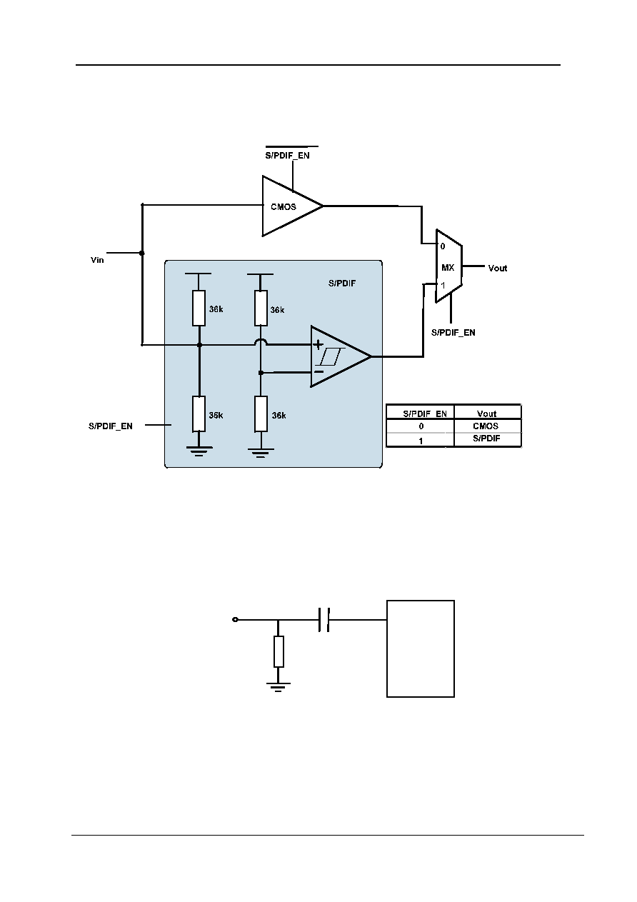
Product Preview
WM8777
w
PP Rev 1.94 November 2004
99
EXTERNAL S/PDIF INPUT CIRCUIT CONFIGURATION
The SPIN, GPIO1, GPIO2, and GPIO3 pads can be configured to accept either CMOS or S/PDIF
input signals. In S/PDIF mode an A.C. coupled input signal is applied to Vin. A hysteresis comparator
buffers this signal and converts it to CMOS to drive on-chip. In CMOS mode the S/PDIF circuit is
disabled and the signal is buffered using standard CMOS logic.
To allow an S/PDIF signal to be received correctly the incoming signal must be A.C. coupled. The
recommended off-chip input configuration for this is shown below:
0.1µF
75
WM8777
Rx
Vin

WM8777
Product Preview
w
PP Rev 1.94 November 2004
100
RECOMMENDED ANALOGUE OUTPUT EXTERNAL COMPONENTS
It may be that a lowpass filter is required to be applied to the output from each DAC channel for Hi Fi
applications. Typically a second order filter is suitable and provides sufficient attenuation of high
frequency components (the unique low order, high bit count multi-bit sigma delta DAC structure used
in WM8777 produces much less high frequency output noise than competitors devices). This filter is
typically also used to provide the 2x gain needed to provide the standard 2Vrms output level from
most consumer equipment. Figure 45 shows a suitable post DAC filter circuit, with 2x gain.
Alternative inverting filter architectures might also be used with as good results.
Figure 45 Recommended Post DAC Filter Circuit
7.5k
1.8k
10uF
1.0nF
47k
4.7k
680pF
4.7k
51
OP_FIL
VOUT1L
OP_FIL
VOUT1R
OP_FIL
VOUT2R
OP_FIL
VOUT2L
OP_FIL
VOUT3L
OP_FIL
VOUT3R
OP_FIL
VOUT4L
OP_FIL
VOUT4R

Product Preview
WM8777
w
PP Rev 1.94 November 2004
101
PACKAGE DIMENSIONS
DM036.A
FT: 100 PIN TQFP (14 x 14 x 1.0 mm)
c
L
E1
D1
D
E
A A2
A1
SEATING PLANE
-C-
0.1 C
e
b
NOTES:
A. ALL LINEAR DIMENSIONS ARE IN MILLIMETERS.
B. THIS DRAWING IS SUBJECT TO CHANGE WITHOUT NOTICE.
C. BODY DIMENSIONS DO NOT INCLUDE MOLD FLASH OR PROTRUSION, NOT TO EXCEED 0.25MM.
D. MEETS JEDEC.95 MS-026, VARIATION = ABA. REFER TO THIS SPECIFICATION FOR FURTHER DETAILS.
Symbols
Dimensions
(mm)
MIN
NOM
MAX
A
-----
-----
1.60
A
1
0.05
-----
0.15
A
2
1.35
1.40
1.45
b
0.17
0.22
0.27
c
-----
-----
0.17
D
16.00
D
1
14.00
E
16.00
E
1
14.00
e
0.50 BSC
L
0.50
0.60
0.75
0
o
3.5
o
7
o
Tolerances of Form and Position
ccc
0.08
REF:
JEDEC.95, MS-026
1
25
26
50
51
74
100
75
15.80
14.05
13.95
15.80
13.95
16.20
11.05
16.20

WM8777
Product Preview
w
PP Rev 1.94 November 2004
102
IMPORTANT NOTICE
Wolfson Microelectronics plc (WM) reserve the right to make changes to their products or to discontinue any product or
service without notice, and advise customers to obtain the latest version of relevant information to verify, before placing
orders, that information being relied on is current. All products are sold subject to the WM terms and conditions of sale
supplied at the time of order acknoPAIFRX_WLedgement, including those pertaining to warranty, patent infringement, and
limitation of liability.
WM warrants performance of its products to the specifications applicable at the time of sale in accordance with WM's
standard warranty. Testing and other quality control techniques are utilised to the extent WM deems necessary to support
this warranty. Specific testing of all parameters of each device is not necessarily performed, except those mandated by
government requirements.
In order to minimise risks associated with customer applications, adequate design and operating safeguards must be used
by the customer to minimise inherent or procedural hazards. Wolfson products are not authorised for use as critical
components in life support devices or systems without the express written approval of an officer of the company. Life
support devices or systems are devices or systems that are intended for surgical implant into the body, or support or
sustain life, and whose failure to perform when properly used in accordance with instructions for use provided, can be
reasonably expected to result in a significant injury to the user. A critical component is any component of a life support
device or system whose failure to perform can be reasonably expected to cause the failure of the life support device or
system, or to affect its safety or effectiveness.
WM assumes no liability for applications assistance or customer product design. WM does not warrant or represent that
any license, either express or implied, is granted under any patent right, copyright, mask work right, or other intellectual
property right of WM covering or relating to any combination, machine, or process in which such products or services might
be or are used. WM's publication of information regarding any third party's products or services does not constitute WM's
approval, license, warranty or endorsement thereof.
Reproduction of information from the WM web site or datasheets is permissible only if reproduction is without alteration and
is accompanied by all associated warranties, conditions, limitations and notices. Representation or reproduction of this
information with alteration voids all warranties provided for an associated WM product or service, is an unfair and deceptive
business practice, and WM is not responsible nor liable for any such use.
Resale of WM's products or services with statements different from or beyond the parameters stated by WM for that
product or service voids all express and any implied warranties for the associated WM product or service, is an unfair and
deceptive business practice, and WM is not responsible nor liable for any such use.
ADDRESS:
Wolfson Microelectronics plc
Westfield House
26 Westfield Road
Edinburgh
EH11 2QB
United Kingdom
Tel :: +44 (0)131 272 7000
Fax :: +44 (0)131 272 7001
Email :: sales@wolfsonmicro.com