Document Outline
- WM8778
- 24-bit,192kHz Stereo Codec
- DESCRIPTION
- FEATURES
- APPLICATIONS
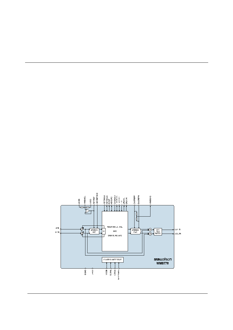
- BLOCK DIAGRAM
- TABLE OF CONTENTS
- PIN CONFIGURATION
- ORDERING INFORMATION
- PIN DESCRIPTION
- ABSOLUTE MAXIMUM RATINGS
- RECOMMENDED OPERATING CONDITIONS
- ELECTRICAL CHARACTERISTICS
- MASTER CLOCK TIMING
- DIGITAL AUDIO INTERFACE Ö MASTER MODE
- DIGITAL AUDIO INTERFACE Ö SLAVE MODE
- 3-WIRE MPU INTERFACE TIMING
- CONTROL INTERFACE TIMING Ö 2--WIRE MODE
- DEVICE DESCRIPTION
- INTRODUCTION
- AUDIO DATA SAMPLING RATES
- ZERO DETECT
- POWERDOWN MODES
- POWER-ON-RESET
- DIGITAL AUDIO INTERFACE
- CONTROL INTERFACE OPERATION
- CONTROL INTERFACE REGISTERS
- LIMITER /AUTOMATIC LEVEL CONTROL (ALC)
- REGISTER MAP
- DIGITAL FILTER CHARACTERISTICS
- DAC FILTER RESPONSES
- ADC FILTER RESPONSES
- ADC HIGH PASS FILTER
- DIGITAL DE-EMPHASIS CHARACTERISTICS
- APPLICATIONS INFORMATION
- RECOMMENDED EXTERNAL COMPONENTS
- PACKAGE DIMENSIONS
- IMPORTANT NOTICE
- ADDRESS:
w
WM8778
24-bit, 192kHz Stereo Codec
WOLFSON MICROELECTRONICS plc
w :: www.wolfsonmicro.com
Product Preview, June 2004, Rev 1.7
Copyright
2004 Wolfson Microelectronics plc
DESCRIPTION
The WM8778 is a high performance, stereo audio codec.
It is ideal for surround sound processing applications for
home hi-fi, DVD-RW and other audio visual equipment.
The stereo 24-bit multi-bit sigma delta ADC has
programmable gain with automatic level control. Digital
audio output word lengths from 16-32 bits and sampling
rates from 32kHz to 96kHz are supported.
A stereo multi-bit sigma delta DAC is used with digital
audio input word lengths from 16-32 bits and sampling
rates from 32kHz to 192kHz. A multiplexor after the DAC
allows the selection of either an external analogue input
or DAC playback into the line outputs.
The WM8778 supports fully independent sample rates
for the ADC and DAC. The audio data interface supports
I
2
S, left justified, right justified and DSP formats.
The device is controlled in software via a 2 or 3 wire
serial interface which provides access to all features
including volume controls, mutes, and de-emphasis
facilities. It can also be controlled in hardware which
gives access to the most commonly used features.
Control interface selection is done via the MODE pin (tri-
level). The device is available in a 28-pin SSOP package.
FEATURES
∑
Audio Performance
-
108dB SNR (`A' weighted @ 48kHz) DAC
-
102dB SNR (`A' weighted @ 48kHz) ADC
∑
DAC Sampling Frequency: 32kHz ≠ 192kHz
∑
ADC Sampling Frequency: 32kHz ≠ 96kHz
∑
Stereo ADC input analogue gain adjust from +24dB to ≠21dB
in 0.5dB steps
∑
ADC digital gain from -21.5dB to -103dB in 0.5dB steps
∑
Programmable Automatic Level Control (ALC) or Limiter on
ADC input.
∑
Stereo DAC with analogue line outputs.
∑
3-Wire SPI Compatible or 2-wire Serial Control Interface
∑
Hardware Control Mode
∑
Master or Slave Clocking Mode
∑
Programmable Audio Data Interface Modes
-
I
2
S, Left, Right Justified or DSP
-
16/20/24/32 bit Word Lengths
∑
Analogue Bypass Path Feature
∑
2.7V to 5.5V Analogue, 2.7V to 3.6V Digital supply Operation
APPLICATIONS
BLOCK DIAGRAM
∑ Surround Sound AV Processors and Hi-Fi systems
∑ DVD-RW

WM8778
Product Preview
w
PP Rev 1.7 June 2004
2
TABLE OF CONTENTS
DESCRIPTION .......................................................................................................1
FEATURES.............................................................................................................1
APPLICATIONS .....................................................................................................1
BLOCK DIAGRAM .................................................................................................1
TABLE OF CONTENTS .........................................................................................2
PIN CONFIGURATION...........................................................................................3
ORDERING INFORMATION ..................................................................................3
ABSOLUTE MAXIMUM RATINGS .........................................................................5
ELECTRICAL CHARACTERISTICS ......................................................................6
TERMINOLOGY ............................................................................................................ 7
MASTER CLOCK TIMING......................................................................................8
DIGITAL AUDIO INTERFACE ≠ MASTER MODE ......................................................... 8
TABLE 2 DIGITAL AUDIO DATA TIMING ≠ MASTER MODE ....................................... 9
DIGITAL AUDIO INTERFACE ≠ SLAVE MODE ............................................................ 9
3-WIRE MPU INTERFACE TIMING ............................................................................ 11
CONTROL INTERFACE TIMING ≠ 2-WIRE MODE .................................................... 12
DEVICE DESCRIPTION .......................................................................................13
INTRODUCTION ......................................................................................................... 13
AUDIO DATA SAMPLING RATES............................................................................... 13
ZERO DETECT ........................................................................................................... 15
POWERDOWN MODES ............................................................................................. 15
POWER-ON-RESET ................................................................................................... 15
DIGITAL AUDIO INTERFACE ..................................................................................... 16
CONTROL INTERFACE OPERATION ........................................................................ 21
CONTROL INTERFACE REGISTERS ........................................................................ 23
LIMITER / AUTOMATIC LEVEL CONTROL (ALC) ...................................................... 32
REGISTER MAP ......................................................................................................... 38
DIGITAL FILTER CHARACTERISTICS ...............................................................45
DAC FILTER RESPONSES......................................................................................... 45
ADC FILTER RESPONSES......................................................................................... 46
ADC HIGH PASS FILTER ........................................................................................... 46
DIGITAL DE-EMPHASIS CHARACTERISTICS........................................................... 47
APPLICATIONS INFORMATION .........................................................................48
RECOMMENDED EXTERNAL COMPONENTS .......................................................... 48
PACKAGE DIMENSIONS ....................................................................................49
IMPORTANT NOTICE ..........................................................................................50
ADDRESS: .................................................................................................................. 50
Product Preview
WM8778
w
PP Rev 1.7 June 2004
3
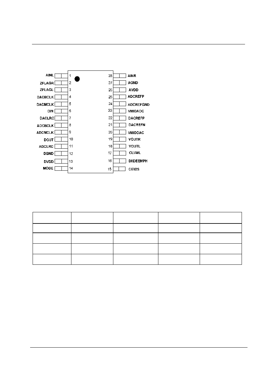
PIN CONFIGURATION
ORDERING INFORMATION
DEVICE
TEMP. RANGE
PACKAGE
MOISTURE
SENSITIVITY LEVEL
PEAK SOLDERING
TEMP
WM8778EDS
-25 to +85
o
C
28-pin SSOP
MSL1
240
∞C
WM8778EDS/R
-25 to +85
o
C
28-pin SSOP
(tape and reel)
MSL1
240
∞C
WM8778SEDS
-25 to +85
o
C
28-pin SSOP
(lead free)
MSL1
260
∞C
WM8778SEDS/R
-25 to +85
o
C
28-pin SSOP
(lead free, tape and reel)
MSL1
260
∞C
Note:
Reel quantity = 2,000
WM8778
Product Preview
w
PP Rev 1.7 June 2004
4
PIN DESCRIPTION
PIN
NAME
TYPE
DESCRIPTION
1
AINL
Analogue Input
Left channel input
2
ZFLAGR
Digital Output
Right channel zero flag output (external pull-up required)
3
ZFLAGL
Digital Output
Left channel zero flag output (external pull-up required)
4
DACBCLK
Digital Input/Output DAC audio interface bit clock
5
DACMCLK
Digital Input
Master DAC clock; 256, 384, 512 or 768fs (fs = word clock frequency)
6
DIN
Digital Input
DAC data input
7
DACLRC
Digital Input/Output DAC left/right word clock
8
ADCBCLK
Digital Input/Output ADC audio interface bit clock
9
ADCMCLK
Digital Input
Master ADC clock; 256, 384, 512 or 768fs (fs = word clock frequency)
10
DOUT
Digital Output
ADC data output
11
ADCLRC
Digital Input/Output ADC left/right word clock
12
DGND
Supply
Digital negative supply
13
DVDD
Supply
Digital positive supply
14
MODE
Digital Input
Control interface mode select, tri-level (5V tolerant)
15
CE\I2S
Digital Input
Serial interface Latch signal (5V tolerant)
16
DI\DEEMPH
Digital Input/Output Serial interface data (5V tolerant)
17
CL\IWL
Digital Input
Serial interface clock (5V tolerant)
18
VOUTL
Analogue Output
DAC channel left output
19
VOUTR
Analogue Output
DAC channel right output
20
VMIDDAC
Analogue Output
DAC midrail decoupling pin ; 10uF external decoupling
21
DACREFN
Analogue Input
DAC negative reference input
22
DACREFP
Analogue Input
DAC positive reference input
23
VMIDADC
Analogue Output
ADC midrail divider decoupling pin; 10uF external decoupling
24
ADCREFGND
Analogue Output
ADC reference buffer decoupling pin; 10uF external decoupling
25
ADCREFP
Analogue Output
ADC positive reference decoupling pin; 10uF external decoupling
26
AVDD
Supply
Analogue positive supply
27
AGND
Supply
Analogue negative supply and substrate connection
28
AINR
Analogue Input
Right channel input
Note : Digital input pins have Schmitt trigger input buffers and pins 14-17 are 5V tolerant.
Product Preview
WM8778
w
PP Rev 1.7 June 2004
5
ABSOLUTE MAXIMUM RATINGS
Absolute Maximum Ratings are stress ratings only. Permanent damage to the device may be caused by continuously operating at
or beyond these limits. Device functional operating limits and guaranteed performance specifications are given under Electrical
Characteristics at the test conditions specified.
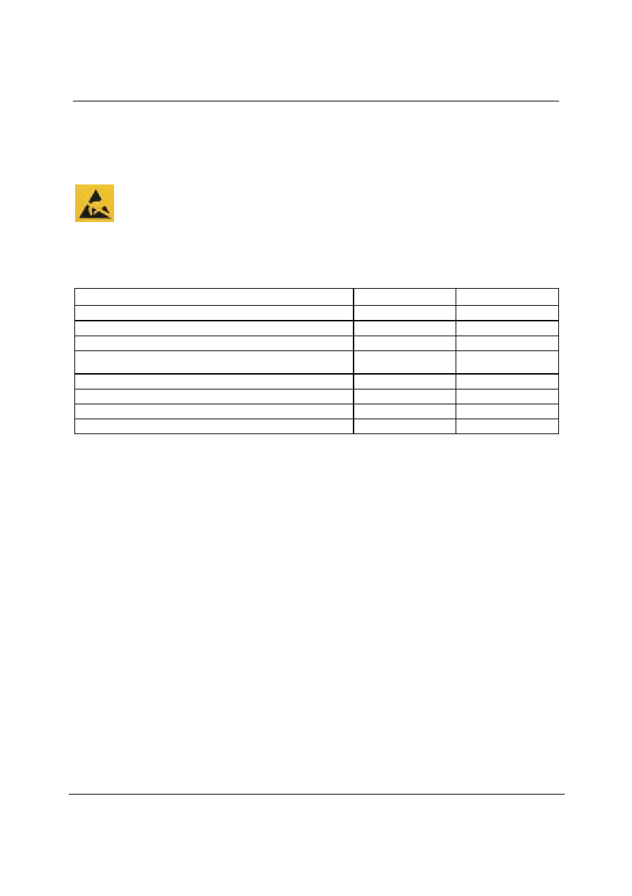
ESD Sensitive Device. This device is manufactured on a CMOS process. It is therefore generically susceptible
to damage from excessive static voltages. Proper ESD precautions must be taken during handling and storage
of this device.
Wolfson tests its package types according to IPC/JEDEC J-STD-020B for Moisture Sensitivity to determine acceptable storage
conditions prior to surface mount assembly. These levels are:
MSL1 = unlimited floor life at <30
∞C / 85% Relative Humidity. Not normally stored in moisture barrier bag.
MSL2 = out of bag storage for 1 year at <30
∞C / 60% Relative Humidity. Supplied in moisture barrier bag.
MSL3 = out of bag storage for 168 hours at <30
∞C / 60% Relative Humidity. Supplied in moisture barrier bag.
CONDITION
MIN
MAX
Digital supply voltage
-0.3V
+3.63V
Analogue supply voltage
-0.3V
+7V
Voltage range digital inputs (DI, CL, CE and MODE)
DGND -0.3V
+7V
Voltage range digital inputs (MCLK, DIN, ADCLRC, DACLRC,
ADCBCLK and DACBCLK)
DGND -0.3V
DVDD + 0.3V
Voltage range analogue inputs
AGND -0.3V
AVDD +0.3V
Master Clock Frequency
37MHz
Operating temperature range, T
A
-25
∞C
+85
∞C
Storage temperature
-65
∞C
+150
∞C
Notes:
1.
Analogue and digital grounds must always be within 0.3V of each other.
WM8778
Product Preview
w
PP Rev 1.7 June 2004
6
RECOMMENDED OPERATING CONDITIONS
PARAMETER
SYMBOL
TEST CONDITIONS
MIN
TYP
MAX
UNIT
Digital supply range
DVDD
2.7
3.6
V
Analogue supply range
AVDD, DACREFP
2.7
5.5
V
Ground
AGND, DGND,
DACREFN,
ADCREFGND
0
V
Difference DGND to AGND
-0.3
0
+0.3
V
Note: Digital supply DVDD must never be more than 0.3V greater than AVDD.
ELECTRICAL CHARACTERISTICS
Test Conditions
AVDD = 5V, DVDD = 3.3V, AGND = 0V, DGND = 0V, T
A
= +25
o
C, fs = 48kHz, MCLK = 256fs unless otherwise stated.
PARAMETER
SYMBOL
TEST CONDITIONS
MIN
TYP
MAX
UNIT
Digital Logic Levels (TTL Levels)
Input LOW level
V
IL
0.8
V
Input HIGH level
V
IH
2.0
V
Output LOW
V
OL
I
OL
=1mA
0.1 x DVDD
V
Output HIGH
V
OH
I
OH
=1mA
0.9 x DVDD
V
Analogue Reference Levels
Reference voltage
V
VMID
AVDD/2
V
Potential divider resistance
R
VMID
50k
DAC Performance (Load
= 10k , 50pF)
0dBFs Full scale output voltage
1.0 x
AVDD/5
Vrms
SNR (Note 1,2)
A-weighted,
@ fs = 48kHz
100
108
dB
SNR (Note 1,2)
A-weighted
@ fs = 96kHz
108
dB
Dynamic Range (Note 2)
DNR
A-weighted, -60dB
full scale input
100
108
dB
Total Harmonic Distortion (THD)
1kHz, 0dBFs
-97
-90
dB
DAC channel separation
100
dB
1kHz 100mVpp
50
dB
Power Supply Rejection Ratio
PSRR
20Hz to 20kHz
100mVpp
45
dB
ADC Performance
Input Signal Level (0dB)
1.0 x
AVDD/5
Vrms
SNR (Note 1,2)
A-weighted, 0dB gain
@ fs = 48kHz
93
102
dB
SNR (Note 1,2)
A-weighted, 0dB gain
@ fs = 96kHz
64 x OSR
99
dB
Dynamic Range (note 2)
A-weighted, -60dB
full scale input
102
dB
1kHz, 0dBFs
-90
dB
Total Harmonic Distortion (THD)
1kHz, -3dBFs
-95
-85
dB
ADC Channel Separation
1kHz Input
90
dB

Product Preview
WM8778
w
PP Rev 1.7 June 2004
7
Test Conditions
AVDD = 5V, DVDD = 3.3V, AGND = 0V, DGND = 0V, T
A
= +25
o
C, fs = 48kHz, MCLK = 256fs unless otherwise stated.
Programmable Gain Step Size
0.25
0.5
0.75
dB
Programmable Gain Range
(Analogue)
1kHz Input
-21
+24
dB
Programmable Gain Range
(Digital)
1kHz Input
-103
-21.5
dB
Mute Attenuation (Note 6)
1kHz Input, 0dB gain
76
dB
1kHz 100mVpp
50
dB
Power Supply Rejection Ratio
PSRR
20Hz to 20kHz
100mVpp
45
dB
Analogue input (AIN) to Analogue output (VOUT) (Load=10k , 50pF, gain = 0dB) Bypass Mode
0dB Full scale output voltage
1.0 x
AVDD/5
Vrms
SNR (Note 1)
90
100
dB
1kHz, 0dB
-90
dB
THD
1kHz, -3dB
-95
dB
1kHz 100mVpp
50
dB
Power Supply Rejection Ratio
PSRR
20Hz to 20kHz
100mVpp
45
dB
Mute Attenuation
1kHz, 0dB
100
dB
Supply Current
Analogue supply current
AVDD = 5V
48
mA
Digital supply current
DVDD = 3.3V
8
mA
Notes:
1.
Ratio of output level with 1kHz full scale input, to the output level with all zeros into the digital input, measured `A'
weighted.
2.
All performance measurements done with 20kHz low pass filter, and where noted an A-weight filter. Failure to use
such a filter will result in higher THD+N and lower SNR and Dynamic Range readings than are found in the Electrical
Characteristics. The low pass filter removes out of band noise; although it is not audible it may affect dynamic
specification values.
3.
VMID decoupled with 10uF and 0.1uF capacitors (smaller values may result in reduced performance).
4.
Harmonic distortion on the headphone output decreases with output power.
5.
All performance measurement done using certain timings conditions (Please refer to section `Digital Audio Interface').
6.
A better MUTE Attenuation can be achieved if the ADC gain is set to minimum.
TERMINOLOGY
1.
Signal-to-noise ratio (dB) - SNR is a measure of the difference in level between the full scale output and the output
with no signal applied. (No Auto-zero or Automute function is employed in achieving these results).
2.
Dynamic range (dB) - DNR is a measure of the difference between the highest and lowest portions of a signal.
Normally a THD+N measurement at 60dB below full scale. The measured signal is then corrected by adding the 60dB
to it. (e.g. THD+N @ -60dB= -32dB, DR= 92dB).
3.
THD+N (dB) - THD+N is a ratio, of the rms values, of (Noise + Distortion)/Signal.
4.
Stop band attenuation (dB) - Is the degree to which the frequency spectrum is attenuated (outside audio band).
5.
Channel Separation (dB) - Also known as Cross-Talk. This is a measure of the amount one channel is isolated from
the other. Normally measured by sending a full scale signal down one channel and measuring the other.
6.
Pass-Band Ripple - Any variation of the frequency response in the pass-band region.
WM8778
Product Preview
w
PP Rev 1.7 June 2004
8
MASTER CLOCK TIMING
MCLK
t
MCLKL
t
MCLKH
t
MCLKY
Figure 1 Master Clock Timing Requirements
Test Conditions
AVDD = 5V, DVDD = 3.3V, AGND = 0V, DGND = 0V, T
A
= +25
o
C, fs = 48kHz, ADC/DACMCLK = 256fs unless otherwise
stated.
PARAMETER
SYMBOL
TEST CONDITIONS
MIN
TYP
MAX
UNIT
System Clock Timing Information
ADC/DACMCLK System clock
pulse width high
t
MCLKH
11
ns
ADC/DACMCLK System clock
pulse width low
t
MCLKL
11
ns
ADC/DACMCLK System clock
cycle time
t
MCLKY
28
ns
ADC/DACMCLK Duty cycle
40:60
60:40
Table 1 Master Clock Timing Requirements
DIGITAL AUDIO INTERFACE ≠ MASTER MODE
ADCBCLK
DOUT
ADCLRC
DIN
DACLRC
WM8778
CODEC
DVD
Controller
DACBCLK
Figure 2 Audio Interface - Master Mode
Product Preview
WM8778
w
PP Rev 1.7 June 2004
9
ADCBCLK/
DACBCLK
(Output)
DOUT
ADCLRC/
DACLRC
(Outputs)
t
DL
DIN
t
DDA
t
DHT
t
DST
Figure 3 Digital Audio Data Timing ≠ Master Mode
Test Conditions
AVDD = 5V, DVDD = 3.3V, AGND = 0V, DGND = 0V, T
A
= +25
o
C, Master Mode, fs = 48kHz, ADC/DACMCLK = 256fs unless
otherwise stated.
PARAMETER
SYMBOL
TEST CONDITIONS
MIN
TYP
MAX
UNIT
Audio Data Input Timing Information
ADC/DACLRC propagation
delay from ADC/DACBCLK
falling edge
t
DL
0
10
ns
DOUT propagation delay
from ADCBCLK falling edge
t
DDA
0
10
ns
DIN setup time to
DACBCLK rising edge
t
DST
10
ns
DIN hold time from
DACBCLK rising edge
t
DHT
10
ns
Table 2 Digital Audio Data Timing ≠ Master Mode
DIGITAL AUDIO INTERFACE ≠ SLAVE MODE
ADCBCLK
DOUT
ADCLRC
DIN
DACLRC
WM8776
CODEC
DVD
Controller
DACBCLK
Figure 4 Audio Interface ≠ Slave Mode

WM8778
Product Preview
w
PP Rev 1.7 June 2004
10
ADCBCLK/
DACBCLK
DACLRC/
ADCLRC
t
BCH
t
BCL
t
BCY
DIN
DOUT
t
LRSU
t
DS
t
LRH
t
DH
t
DD
Figure 5 Digital Audio Data Timing ≠ Slave Mode
Test Conditions
AVDD = 5V, DVDD = 3.3V, AGND = 0V, DGND = 0V, T
A
= +25
o
C, Slave Mode, fs = 48kHz, ADC/DACMCLK = 256fs unless
otherwise stated.
PARAMETER
SYMBOL
TEST CONDITIONS
MIN
TYP
MAX
UNIT
Audio Data Input Timing Information
ADC/DACBCLK cycle time
t
BCY
50
ns
ADC/DACBCLK pulse width
high
t
BCH
20
ns
ADC/DACBCLK pulse width
low
t
BCL
20
ns
DACLRC/ADCLRC set-up
time to ADC/DACBCLK
rising edge
t
LRSU
10
ns
DACLRC/ADCLRC hold
time from ADC/DACBCLK
rising edge
t
LRH
10
ns
DIN set-up time to
DACBCLK rising edge
t
DS
10
ns
DIN hold time from
DACBCLK rising edge
t
DH
10
ns
DOUT propagation delay
from ADCBCLK falling edge
t
DD
0
10
ns
Table 3 Digital Audio Data Timing ≠ Slave Mode
Note:
ADCLRC and DACLRC should be synchronous with MCLK, although the WM8778 interface is tolerant of phase variations
or jitter on these signals.

Product Preview
WM8778
w
PP Rev 1.7 June 2004
11
3-WIRE MPU INTERFACE TIMING
CE
CL
DI
t
CSL
t
DHO
t
DSU
t
CSH
t
SCY
t
SCH
t
SCL
t
SCS
LSB
t
CSS
Figure 6 SPI Compatible (3-wire) Control Interface Input Timing (MODE=1)
Test Conditions
AVDD = 5V, DVDD = 3.3V, AGND, DGND = 0V, T
A
= +25
o
C, fs = 48kHz, MCLK = 256fs unless otherwise stated
PARAMETER
SYMBOL
MIN
TYP
MAX
UNIT
CL rising edge to CE rising edge
t
SCS
60
ns
CL pulse cycle time
t
SCY
80
ns
CL pulse width low
t
SCL
30
ns
CL pulse width high
t
SCH
30
ns
DI to CL set-up time
t
DSU
20
ns
CL to DI hold time
t
DHO
20
ns
CE pulse width low
t
CSL
20
ns
CE pulse width high
t
CSH
20
ns
CE rising to CL rising
t
CSS
20
ns
Table 4 3-wire SPI Compatible Control Interface Input Timing Information
WM8778
Product Preview
w
PP Rev 1.7 June 2004
12
CONTROL INTERFACE TIMING ≠ 2-WIRE MODE
t
3
t
1
t
6
t
9
t
2
t
5
t
7
t
3
t
4
t
8
DI
CL
Figure 7 Control Interface Timing ≠ 2-Wire Serial Control Mode (MODE=0)
Test Conditions
AVDD = 5V, DVDD = 3.3V, AGND, DGND = 0V, T
A
= +25
o
C, fs = 48kHz, MCLK = 256fs unless otherwise stated
PARAMETER
SYMBOL
MIN
TYP
MAX
UNIT
Program Register Input Information
CL Frequency
0
400
kHz
CL Low Pulse-Width
t
1
600
ns
CL High Pulse-Width
t
2
1.3
us
Hold Time (Start Condition)
t
3
600
ns
Setup Time (Start Condition)
t
4
600
ns
Data Setup Time
t
5
100
ns
DI, CL Rise Time
t
6
300
ns
DI, CL Fall Time
t
7
300
ns
Setup Time (Stop Condition)
t
8
600
ns
Data Hold Time
t
9
900
ns
Pulse width of spikes that will be suppressed
t
ps
0
5
ns
Table 5 2-wire Control Interface Timing Information

Product Preview
WM8778
w
PP Rev 1.7 June 2004
13
DEVICE DESCRIPTION
INTRODUCTION
WM8778 is a complete 2-channel DAC, 2-channel ADC audio codec, including digital interpolation
and decimation filters, multi-bit sigma delta stereo ADC, and switched capacitor multi-bit sigma delta
DACs with output smoothing filters. It is available in a single package and controlled by a 3 or 2-wire
serial interface or in a hardware mode.
An analogue bypass path option is available, to allow stereo analogue signals from the stereo inputs
to be sent to the stereo outputs. This allows a purely analogue input to analogue output high quality
signal path to be implemented if required.
The DAC and ADC have separate left/right clocks, bit clocks, master clocks and data I/Os. The
Audio Interface may be configured to operate in either master or slave mode. In Slave mode
ADCLRC, DACLRC, ADCBCLK and DACBCLK are all inputs. In Master mode ADCLRC, DACLRC,
ADCBCLK and DACBCLK are outputs.
The ADC has an analogue input PGA and a digital gain control, accessed by one register write. The
input PGA allows input signals to be gained up to +24dB and attenuated down to -21dB in 0.5dB
steps. The digital gain control allows attenuation from -21.5dB to -103dB in 0.5dB steps. This allows
the user maximum flexibility in the use of the ADC.
The DAC has its own digital volume control, which is adjustable between 0dB and -127.5dB in 0.5dB
steps. In addition a zero cross detect circuit is provided for digital volume controls. The digital
volume control detects a transition through the zero point before updating the volume. This
minimises audible clicks and `zipper' noise as the gain values change.
The DAC output incorporates an input selector and mixer allowing a signal to be either switched into
the signal path in place of the DAC signal or mixed with the DAC signal before the analogue outputs.
Control of internal functionality of the device can be by 3-wire SPI compatible or 2-wire serial control
interface, or hardware mode, selected by the MODE pin. Both interfaces may be asynchronous to the
audio data interface as control data will be re-synchronised to the audio processing internally.
CE, CL, DI and MODE are 5V tolerant with TTL input thresholds, allowing the WM8778 to used with
DVDD = 3.3V and be controlled by a controller with 5V output.
Operation using system clock of 128fs, 192fs, 256fs, 384fs, 512fs or 768fs is provided. In Slave
mode selection between clock rates is automatically controlled. In master mode the master clock to
sample rate ratio is set by control bits ADCRATE and DACRATE. ADC and DAC may run at different
rates. Master clock sample rates (fs) from less than 32kHz up to 192kHz are allowed, provided the
appropriate system clock is input.
The audio data interface supports right, left and I
2
S interface formats along with a highly flexible DSP
serial port interface.
AUDIO DATA SAMPLING RATES
In a typical digital audio system there is only one central clock source producing a reference clock to
which all audio data processing is synchronised. This clock is often referred to as the audio system's
Master Clock. The WM8778 uses separate master clocks for the ADC and DAC. The external master
system clocks can be applied directly through the ADCMCLK and DACMCLK input pins with no
software configuration necessary. In a system where there are a number of possible sources for the
reference clock it is recommended that the clock source with the lowest jitter be used to optimise the
performance of the ADC and DAC.
The master clock for WM8778 supports DAC audio sampling rates from 128fs to 768fs and ADC
sampling rates from 256fs to 512fs, where fs is the audio sampling frequency (DACLRC or ADCLRC)
typically 32kHz, 44.1kHz, 48kHz or 96kHz. The master clock is used to operate the digital filters and
the noise shaping circuits.
In Slave mode the WM8778 has a master detection circuit that automatically determines the
relationship between the master clock frequency and the sampling rate (to within +/- 32 system
clocks). If there is a greater than 32 clocks error the interface is disabled and maintains the output
level at the last sample. The master clock must be synchronised with ADCLRC/DACLRC, although
the WM8778 is tolerant of phase variations or jitter on this clock. Table 6 shows the typical master
clock frequency inputs for the WM8778.
WM8778
Product Preview
w
PP Rev 1.7 June 2004
14
The signal processing for the WM8778 typically operates at an oversampling rate of 128fs for both
ADC and DAC. The exception to this for the DAC is for operation with a 128/192fs system clock, e.g.
for 192kHz operation where the oversampling rate is 64fs. For ADC operation at 96kHz it is
recommended that the user set the ADCOSR bit. This changes the ADC signal processing
oversample rate to 64fs.
System Clock Frequency (MHz)
128fs
192fs
SAMPLING
RATE
(DACLRC/
ADCLRC)
DAC ONLY
256fs
384fs
512fs
768fs
32kHz
4.096
6.144
8.192
12.288
16.384
24.576
44.1kHz
5.6448
8.467
11.2896
16.9340
22.5792
33.8688
48kHz
6.144
9.216
12.288
18.432
24.576
36.864
96kHz
12.288
18.432
24.576
36.864
Unavailable Unavailable
192kHz
24.576
36.864
Unavailable Unavailable Unavailable Unavailable
Table 6 System Clock Frequencies Versus Sampling Rate
In Master mode DACBCLK, ADCBCLK, DACLRC and ADCLRC are generated by the WM8778. The
frequencies of ADCLRC and DACLRC are set by setting the required ratio of DACMCLK to DACLRC
and ADCMCLK to ADCLRC using the DACRATE and ADCRATE control bits (Table 7).
ADCRATE[2:0]/
DACRATE[2:0]
ADCMCLK/DACMCLK:
ADCLRC/DACLRC
RATIO
000
128fs (DAC Only)
001
192fs (DAC Only)
010
256fs
011
384fs
100
512fs
101
768fs
Table 7 Master Mode MCLK:ADCLRC/DACLRC Ratio Select
Table 8 shows the settings for ADCRATE and DACRATE for common sample rates and
ADCMCLK/DACMCLK frequencies.
System Clock Frequency (MHz)
128fs
192fs
256fs
384fs
512fs
768fs
SAMPLING
RATE
(DACLRC/
ADCLRC)
DACRATE
=000
DACRATE
=001
ADCRATE/
DACRATE
=010
ADCRATE/
DACRATE
=011
ADCRATE/
DACRATE
=100
ADCRATE/
DACRATE
=101
32kHz
4.096
6.144
8.192
12.288
16.384
24.576
44.1kHz
5.6448
8.467
11.2896
16.9340
22.5792
33.8688
48kHz
6.144
9.216
12.288
18.432
24.576
36.864
96kHz
12.288
18.432
24.576
36.864
Unavailable Unavailable
192kHz
24.576
36.864
Unavailable Unavailable Unavailable Unavailable
Table 8 Master Mode ADC/DACLRC Frequency Selection
Product Preview
WM8778
w
PP Rev 1.7 June 2004
15
ADCBCLK and DACBCLK are also generated by the WM8778. The frequency of ADCBCLK and
DACBCLK depends on the mode of operation.
In 128/192fs modes (DACRATE=000 or 001) BCLK = MCLK/2. In 256/384/512fs modes
(ADCRATE/DACRATE=010 or 011 or 100) BCLK = MCLK/4. However if DSP mode is selected as
the audio interface mode then BCLK=MCLK. Note that DSP mode cannot be used in 128fs mode for
word lengths greater than 16 bits or in 192fs mode for word lengths greater than 24 bits.
ZERO DETECT
The WM8778 has a zero detect circuit for each DAC channel, which detects when 1024 consecutive
zero samples have been input. The two zero flag outputs (ZFLAGL and ZFLAGR) may be
programmed to output the zero detect signals (see Table 9) that may then be used to control external
muting circuits. A `1' on ZFLAGL or ZFLAGR indicates a zero detect. The zero detect may also be
used to automatically enable the mute by setting IZD. The zero flag output may be disabled by
setting DZFM to 00.
DZFM[1:0]
ZFLAGL
ZFLAGR
00
Zero flag disabled
Zero flag disabled
01
Left channel zero
Right channel zero
10
Both channel zero
Both channel zero
11
Either channels zero
Either channel zero
Table 9 Zero Flag Output Select
POWERDOWN MODES
The WM8778 has powerdown control bits allowing specific parts of the WM8778 to be powered off
when not being used. Control bit ADCPD powers off the ADC. The ADC input PGAs will be powered
down only if ADCPD and AINPD are set. When AINPD is set the bypass path is automatically
disabled. The stereo DAC has a separate powerdown control bit, DACPD allowing the DAC to be
powered off when not in use. This also switches the analogue outputs VOUTL/R to VMIDDAC to
maintain a dc level on the output. The output mixer will be disabled when PDWN is set.
Setting AINPD, ADCPD and DACPD will powerdown everything except the references VMIDADC,
ADCREF and VMIDDAC. ADCREF and VMIDDAC can be powered down by setting PDWN,
VMIDADC is always active. Setting PDWN will override all other powerdown control bits. It is
recommended that AINPD, ADCPD and DACPD are set before setting PDWN. The default is for all
blocks to be enabled.
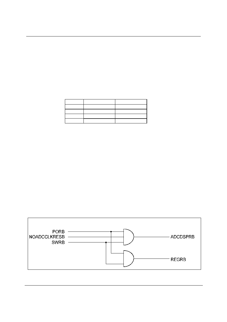
POWER-ON-RESET
The WM8776 has an internal power-on-reset circuit. The reset phase is entered at power-up of
supplies. The DAC and ADC DSP circuitry is also reset when their respective master clocks are
stopped. Register values are maintained unless either a power-on-reset occurs or a software reset is
written. A software reset will also cause a reset of the DAC and ADC DSP. Figure 8 shows the
power-on-reset logic, and Figure 9 shows the reset release characteristics.
Figure 8 Circuit Diagram for Power-on-Reset

WM8778
Product Preview
w
PP Rev 1.7 June 2004
16
Figure 9 Timing Diagram for Power on Sequence
DIGITAL AUDIO INTERFACE
MASTER AND SLAVE MODES
The audio interface operates in either Slave or Master mode, selectable using the MS control bit. In
both Master and Slave modes DIN is always an input to the WM8778 and DOUT is always an output.
The default is Slave mode.
In Slave mode (MS=0) ADCLRC, DACLRC, ADCBCLK and DACBCLK are inputs to the WM8778
(Figure 10). DIN and DACLRC are sampled by the WM8778 on the rising edge of DACBCLK,
ADCLRC is sampled on the rising edge of ADCBCLK. ADC data is output on DOUT and changes on
the falling edge of ADCBCLK. By setting control bit BCLKINV the polarity of ADCBCLK and
DACBCLK may be reversed so that DIN and DACLRC are sampled on the falling edge of DACBCLK,
ADCLRC is sampled on the falling edge of ADCBCLK and DOUT changes on the rising edge of
ADCBCLK.
ADCBCLK
DOUT
ADCLRC
DIN
DACLRC
WM8778
CODEC
DVD
Controller
DACBCLK
Figure 10 Slave Mode
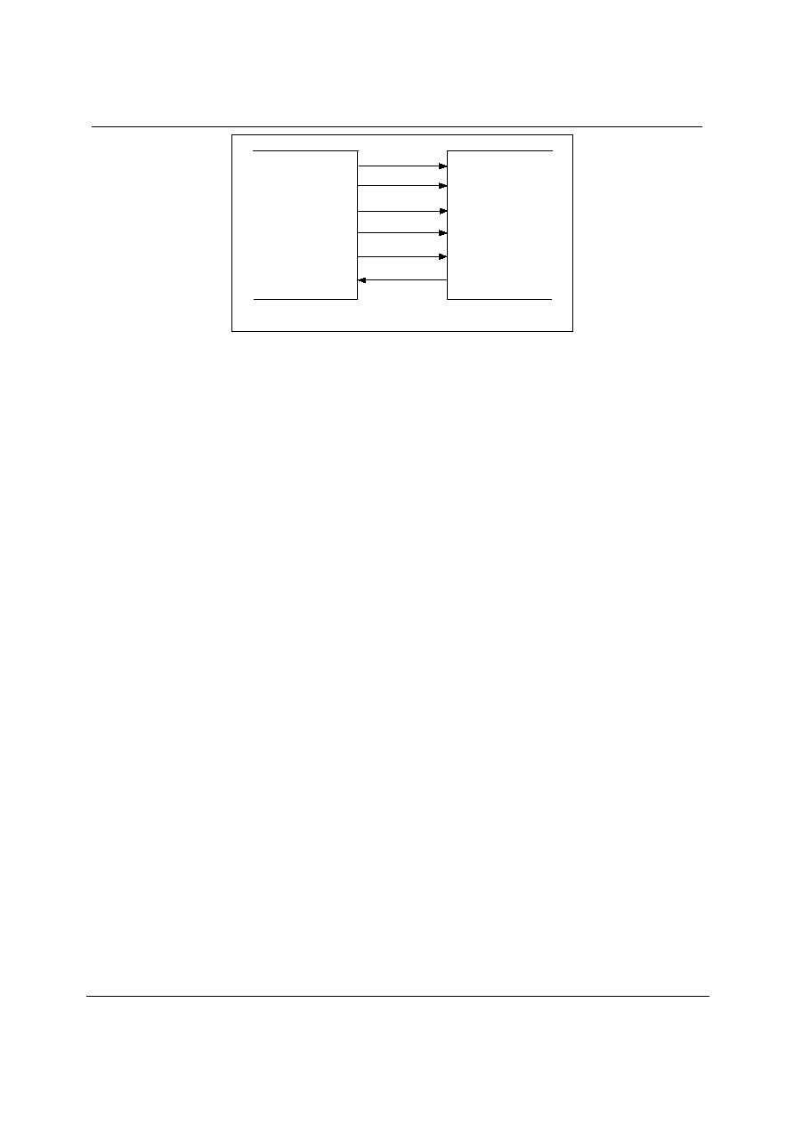
In Master mode (MS=1) ADCLRC, DACLRC, ADCBCLK and DACBCLK are outputs from the
WM8778 (Figure 11). ADCLRC, DACLRC, ADCBCLK and DACBCLK are generated by the WM8778.
DIN is sampled by the WM8778 on the rising edge of DACBCLK so the controller must output DAC
data that changes on the falling edge of DACBCLK. ADC data is output on DOUT and changes on
the falling edge of ADCBCLK. By setting control bit BCLKINV, the polarity of ADCBCLK and
DACBCLK may be reversed so that DIN is sampled on the falling edge of DACBCLK and DOUT
changes on the rising edge of ADCBCLK.
Product Preview
WM8778
w
PP Rev 1.7 June 2004
17
ADCBCLK
DOUT
ADCLRC
DIN
DACLRC
WM8778
CODEC
DVD
Controller
DACBCLK
Figure 11 Master Mode
AUDIO INTERFACE FORMATS
Audio data is applied to the internal DAC filters or output from the ADC filters, via the Digital Audio
Interface. 5 popular interface formats are supported:
∑
Left Justified mode
∑
Right Justified mode
∑
I
2
S mode
∑
DSP Early mode
∑
DSP Late mode
All 5 formats send the MSB first and support word lengths of 16, 20, 24 and 32 bits, with the
exception of 32 bit right justified mode, which is not supported.
In left justified, right justified and I
2
S modes, the digital audio interface receives DAC data on the DIN
input and outputs ADC data on DOUT. Audio Data for each stereo channel is time multiplexed with
ADCLRC/DACLRC indicating whether the left or right channel is present. ADCLRC/DACLRC is also
used as a timing reference to indicate the beginning or end of the data words.
In left justified, right justified and I
2
S modes; the minimum number of BCLKs per DACLRC/ADCLRC
period is 2 times the selected word length. ADCLRC/DACLRC must be high for a minimum of word
length BCLKs and low for a minimum of word length BCLKs. Any mark to space ratio on
ADCLRC/DACLRC is acceptable provided the above requirements are met.
In DSP early or DSP late mode, DACLRC is used as a frame sync signal to identify the MSB of the
first word. The minimum number of DACBCLKs per DACLRC period is 2 times the selected word
length. Any mark to space ratio is acceptable on DACLRC provided the rising edge is correctly
positioned. The ADC data may also be output in DSP early or late modes, with ADCLRC used as a
frame sync to identify the MSB of the first word. The minimum number of ADCBCLKs per ADCLRC
period is 2 times the selected word length.

WM8778
Product Preview
w
PP Rev 1.7 June 2004
18
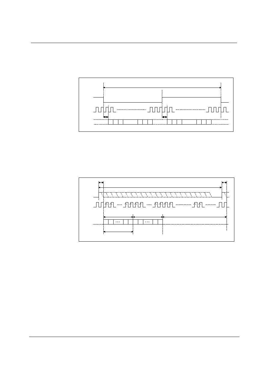
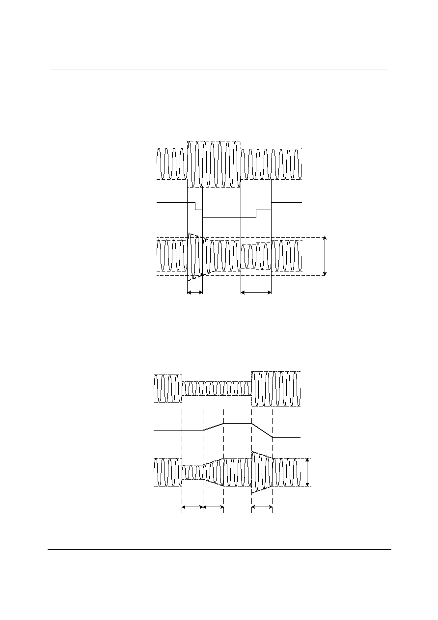
LEFT JUSTIFIED MODE
In left justified mode, the MSB of DIN is sampled by the WM8778 on the first rising edge of
DACBCLK following a DACLRC transition. The MSB of the ADC data is output on DOUT and
changes on the same falling edge of ADCBCLK as ADCLRC and may be sampled on the rising edge
of ADCBCLK. ADCLRC and DACLRC are high during the left samples and low during the right
samples (Figure 12).
LEFT CHANNEL
RIGHT CHANNEL
DACLRC/
ADCLRC
DACBCLK/
ADCBCLK
DIN/
DOUT
1/fs
n
3
2
1
n-2 n-1
LSB
MSB
n
3
2
1
n-2 n-1
LSB
MSB
Figure 12 Left Justified Mode Timing Diagram
RIGHT JUSTIFIED MODE
In right justified mode, the LSB of DIN is sampled by the WM8778 on the rising edge of DACBCLK
preceding a DACLRC transition. The LSB of the ADC data is output on DOUT and changes on the
falling edge of ADCBCLK preceding a ADCLRC transition and may be sampled on the rising edge of
ADCBCLK. ADCLRC and DACLRC are high during the left samples and low during the right samples
(Figure 13).
LEFT CHANNEL
RIGHT CHANNEL
DACLRC/
ADCLRC
DACBCLK/
ADCBCLK
DIN/
DOUT
1/fs
n
3
2
1
n-2 n-1
LSB
MSB
n
3
2
1
n-2 n-1
LSB
MSB
Figure 13 Right Justified Mode Timing Diagram
Product Preview
WM8778
w
PP Rev 1.7 June 2004
19
I
2
S MODE
In I
2
S mode, the MSB of DIN is sampled by the WM8778 on the second rising edge of DACBCLK
following a DACLRC transition. The MSB of the ADC data is output on DOUT and changes on the
first falling edge of ADCBCLK following an ADCLRC transition and may be sampled on the rising
edge of ADCBCLK. ADCLRC and DACLRC are low during the left samples and high during the right
samples.
LEFT CHANNEL
RIGHT CHANNEL
DACLRC/
ADCLRC
DACBCLK/
ADCBCLK
DIN/
DOUT
1/fs
n
3
2
1
n-2 n-1
LSB
MSB
n
3
2
1
n-2 n-1
LSB
MSB
1 BCLK
1 BCLK
Figure 14 I
2
S Mode Timing Diagram
DSP EARLY MODE
In DSP early mode, the MSB of DAC left data is sampled by the WM8778 on the second rising edge
on DACBCLK following a DACLRC rising edge. DAC right data follows DAC channel left data (Figure
15).
DACLRC
DACBCLK
DIN
Word Length (WL)
1/fs
LEFT CHANNEL
n
2
1
n-1
LSB
MSB
n
2
1
n-1
RIGHT CHANNEL
NO VALID DATA
1 BCLK
1 BCLK
Figure 15 DSP Early Mode Timing Diagram ≠ DAC Data Input

WM8778
Product Preview
w
PP Rev 1.7 June 2004
20
The MSB of the left channel ADC data is output on DOUT and changes on the first falling edge of
ADCBCLK following a low to high ADCLRC transition and may be sampled on the rising edge of
ADCBCLK. The right channel ADC data is contiguous with the left channel data (Figure 16)
ADCLRC
ADCBCLK
DOUT
Word Length (WL)
1/fs
LEFT CHANNEL
n
2
1
n-1
LSB
MSB
n
2
1
n-1
RIGHT CHANNEL
NO VALID DATA
1 BCLK
1 BCLK
Figure 16 DSP Early Mode Timing Diagram ≠ ADC Data Output
DSP LATE MODE
In DSP late mode, the MSB of DAC left data is sampled by the WM8778 on the first DACBCLK rising
edge following a DACLRC rising edge. DAC right follow DAC left data (Figure 17).
DACLRC
DACBCLK
DIN
Word Length (WL)
1/fs
LEFT CHANNEL
n
2
1
n-1
LSB
MSB
n
2
1
n-1
RIGHT CHANNEL
NO VALID DATA
1
Figure 17 DSP Late Mode Timing Diagram ≠ DAC Data Input

Product Preview
WM8778
w
PP Rev 1.7 June 2004
21
The MSB of the left channel ADC data is output on DOUT and changes on the same falling edge of
ADCBCLK as the low to high ADCLRC transition and may be sampled on the rising edge of
ADCBCLK. The right channel ADC data is contiguous with the left channel data (Figure 18).
ADCLRC
ADCBCLK
DOUT
Word Length (WL)
1/fs
LEFT CHANNEL
n
2
1
n-1
LSB
MSB
n
2
1
n-1
RIGHT CHANNEL
NO VALID DATA
1
Figure 18 DSP Late Mode Timing Diagram ≠ ADC Data Output
In both early and late DSP modes, the left channel is always sent first, followed immediately by the
right channel. No DACBCLK edges are allowed between the data words.
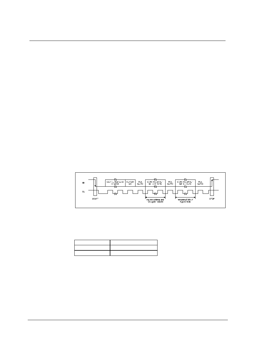
CONTROL INTERFACE OPERATION
The WM8778 is controlled by writing to registers through a serial control interface. A control word
consists of 16 bits. The first 7 bits (B15 to B9) are address bits that select which control register is
accessed. The remaining 9 bits (B8 to B0) are data bits, corresponding to the 9 bits in each control
register. The control interface can operate as either a 3-wire or 2-wire MPU interface. The MODE pin
selects the interface format, as shown in Table 10.
MODE
CONTROL MODE
0
2 wire software
Z / midrail
Hardware
1
3 wire software
Table 10 Control Interface Selection via MODE Pin
The control interface is 5V tolerant, meaning that the control interface input signals CE, CL and DI as
well as MODE may have an input high level of 5V while DVDD is 3V. Input thresholds are determined
by DVDD.
3-WIRE (SPI COMPATIBLE) SERIAL CONTROL MODE
In 3-wire mode, every rising edge of CL clocks in one data bit from the DI pin. A rising edge on CE
latches in a complete control word consisting of the last 16 bits. The 3-wire interface protocol is
shown in Figure 19.
Figure 19 3-wire SPI Compatible Interface
B15
B14
B13
B12
B11
B10
B9
B8
B7
B6
B5
B4
B3
B2
B1
B0
DI
CL
CE
control register address
control register data bits
latch
WM8778
Product Preview
w
PP Rev 1.7 June 2004
22
1.
B[15:9] are Control Address Bits
2.
B[8:0] are Control Data Bits
3.
CE is edge sensitive ≠ the data is latched on the rising edge of CE.
2-WIRE SERIAL CONTROL MODE
The WM8778 supports software control via a 2-wire serial bus. Many devices can be controlled by
the same bus, and each device has a unique 7-bit address (this is not the same as the 7-bit address
of each register in the WM8778).
The WM8778 operates as a slave device only. The controller indicates the start of data transfer with
a high to low transition on DI while CL remains high. This indicates that a device address and data
will follow. All devices on the 2-wire bus respond to the start condition and shift in the next eight bits
on DI (7-bit address + Read/Write bit, MSB first). If the device address received matches the address
of the WM8778 and the R/W bit is `0', indicating a write, then the WM8778 responds by pulling DI low
on the next clock pulse (ACK). If the address is not recognised or the R/W bit is `1', the WM8778
returns to the idle condition and wait for a new start condition and valid address.
Once the WM8778 has acknowledged a correct address, the controller sends the first byte of control
data (B15 to B8, i.e. the WM8778 register address plus the first bit of register data). The WM8778
then acknowledges the first data byte by pulling DI low for one clock pulse. The controller then sends
the second byte of control data (B7 to B0, i.e. the remaining 8 bits of register data), and the WM8778
acknowledges again by pulling DI low.
The transfer of data is complete when there is a low to high transition on DI while CL is high. After
receiving a complete address and data sequence the WM8778 returns to the idle state and waits for
another start condition. If a start or stop condition is detected out of sequence at any point during
data transfer (i.e. DI changes while CL is high), the device jumps to the idle condition.
Figure 20 2-wire Serial Interface
1.
B[15:9] are Control Address Bits
2.
B[8:0] are Control Data Bits
The WM8778 has two possible device addresses, which can be selected using the CE pin.
CE STATE
DEVICE ADDRESS
Low
0011010 (0 x 34h)
High
0011011 (0 x 36h)
Table 11 2-Wire MPU Interface Address Selection
Product Preview
WM8778
w
PP Rev 1.7 June 2004
23
HARDWARE MODE
Hardware mode is selected by applying a midrail voltage to the MODE pin, or by leaving it floating.
The circuit detects this condition and enables hardware mode. This allows limited control of the
internal functions using the three inputs CE, CL and DI. The table below gives a summary of the use
of each pin in hardware mode.
PIN NAME
FUNCTION
DESCRIPTION
CE\I2S
Interface Mode select
0 : Right Justified
1 : I
2
S
CL\IWL
Interface Wordlength select
0 : 20 bit (RJ), 16 bit (I
2
S)
1 : 24 bit
DI\DEEMPH
De-emphasis on/off
0 : De-emphasis disabled
1 : De-emphasis enabled
Table 12 Hardware Mode Functions
CONTROL INTERFACE REGISTERS
DIGITAL AUDIO INTERFACE CONTROL REGISTER
Interface format is selected via the FMT[1:0] register bits:
REGISTER ADDRESS
BIT
LABEL
DEFAULT
DESCRIPTION
R10 (0Ah)
0001010
DAC Interface Control
1:0
DACFMT
[1:0]
10
R11 (0Bh)
0001011
ADC Interface Control
1:0
ADCFMT
[1:0]
10
Interface format Select
00 : right justified mode
01: left justified mode
10: I
2
S mode
11: DSP (early or late) mode
In left justified, right justified or I
2
S modes, the LRP register bit controls the polarity of
ADCLRC/DACLRC. If this bit is set high, the expected polarity of ADCLRC/DACLRC will be the
opposite of that shown Figure 12, Figure 13, etc. Note that if this feature is used as a means of
swapping the left and right channels, a 1 sample phase difference will be introduced. In DSP modes,
the LRP register bit is used to select between early and late modes.
REGISTER ADDRESS
BIT
LABEL
DEFAULT
DESCRIPTION
R10 (0Ah)
0001010
DAC Interface Control
2
DACLRP
0
R11 (0Bh)
0001011
ADC Interface Control
2
ADCLRP
0
In left/right/ I
2
S modes:
ADCLRC/DACLRC Polarity (normal)
0 : normal ADCLRC/DACLRC
polarity
1: inverted ADCLRC/DACLRC
polarity
In DSP mode:
0 : Early DSP mode
1: Late DSP mode
By default, ADCLRC, DACLRC and DIN are sampled on the rising edge of ADCBCLK and
DACBCLK and should ideally change on the falling edge. Data sources that change
ADCLRC/DACLRC and DIN on the rising edge of ADCBCLK/DACBCLK can be supported by setting
the BCP register bit. Setting BCP to 1 inverts the polarity of BCLK to the inverse of that shown in
Figure 12, Figure 13, etc.
REGISTER ADDRESS
BIT
LABEL
DEFAULT
DESCRIPTION
R10 (0Ah)
0001010
DAC Interface Control
3
DACBCP
0
R11 (0Bh)
0001011
ADC Interface Control
3
ADCBCP
0
BCLK Polarity (DSP modes)
0 : normal BCLK polarity
1: inverted BCLK polarity
WM8778
Product Preview
w
PP Rev 1.7 June 2004
24
The WL[1:0] bits are used to control the input word length.
REGISTER ADDRESS
BIT
LABEL
DEFAULT
DESCRIPTION
R10 (0Ah)
0001010
DAC Interface Control
5:4
DACWL
[1:0]
10
R11 (0Bh)
0001011
ADC Interface Control
5:4
ADCWL
[1:0]
10
Word Length
00 : 16 bit data
01: 20 bit data
10: 24 bit data
11: 32 bit data
Note: If 32-bit mode is selected in right justified mode, the WM8778 defaults to 24 bits.
In all modes, the data is signed 2's complement. The digital filters always input 24-bit data. If the
DAC is programmed to receive 16 or 20 bit data, the WM8778 pads the unused LSBs with zeros. If
the DAC is programmed into 32 bit mode, the 8 LSBs are ignored.
Note: In 24 bit I
2
S mode, any width of 24 bits or less is supported provided that ADCLRC/DACLRC is
high for a minimum of 24 BCLKs and low for a minimum of 24 BCLKs.
A number of options are available to control how data from the Digital Audio Interface is applied to
the DAC.
MASTER MODES
Control bit ADCMS selects between audio interface Master and Slave Modes for ADC. In ADC
Master mode ADCLRC and ADCBCLK are outputs and are generated by the WM8778. In Slave
mode ADCLRC and ADCBCLK are inputs to WM8778.
REGISTER ADDRESS
BIT
LABEL
DEFAULT
DESCRIPTION
R12 (0Ch)
0001100
Interface Control
8
ADCMS
0
Audio Interface Master/Slave Mode
select for ADC:
0 : Slave Mode
1: Master Mode
Control bit DACMS selects between audio interface Master and Slave Modes for the DAC. In DAC
Master mode DACLRC and DACBCLK are outputs and are generated by the WM8778. In Slave
mode DACLRC and DACBCLK are inputs to WM8778.
REGISTER ADDRESS
BIT
LABEL
DEFAULT
DESCRIPTION
R12 (0Ch)
0001100
Interface Control
7
DACMS
0
Audio Interface Master/Slave Mode
select for DAC:
0 : Slave Mode
1: Master Mode

Product Preview
WM8778
w
PP Rev 1.7 June 2004
25
MASTER MODE ADCLRC/DACLRC FREQUENCY SELECT
In ADC Master mode the WM8778 generates ADCLRC and ADCBCLK, in DAC master mode the
WM8778 generates DACLRC and DACBCLK. These clocks are derived from the master clock
(ADCMCLK or DACMCLK). The ratios of ADCMCLK to ADCLRC and DACMCLK to DACLRC are
set by ADCRATE and DACRATE respectively.
REGISTER ADDRESS
BIT
LABEL
DEFAULT
DESCRIPTION
2:0
ADCRATE[2:0]
010
Master Mode MCLK:ADCLRC
Ratio Select:
010: 256fs
011: 384fs
100: 512fs
101: 768fs
R12 (0Ch)
0001100
ADCLRC and DACLRC
Frequency Select
6:4
DACRATE[2:0]
010
Master Mode MCLK:DACLRC
Ratio Select:
000: 128fs
001: 192fs
010: 256fs
011: 384fs
100: 512fs
101: 768fs
ADC OVERSAMPLING RATE SELECT
For ADC operation at 96kHz it is recommended that the user set the ADCOSR bit. This changes the
ADC signal processing oversample rate to 64fs.
REGISTER ADDRESS
BIT
LABEL
DEFAULT
DESCRIPTION
R12 (0Ch)
0001100
ADC Oversampling Rate
3
ADCOSR
0
ADC Oversampling Rate Select
0: 128x oversampling
1: 64x oversampling
MUTE MODES
Setting MUTE for the DAC will apply a `soft' mute to the input of the digital filters of the channel
muted.
REGISTER ADDRESS
BIT
LABEL
DEFAULT
DESCRIPTION
R8 (08h)
0001000
DAC Mute
0
DMUTE
0
DAC Soft Mute Select
0 : Normal Operation
1: Soft mute enabled
WM8778
Product Preview
w
PP Rev 1.7 June 2004
26
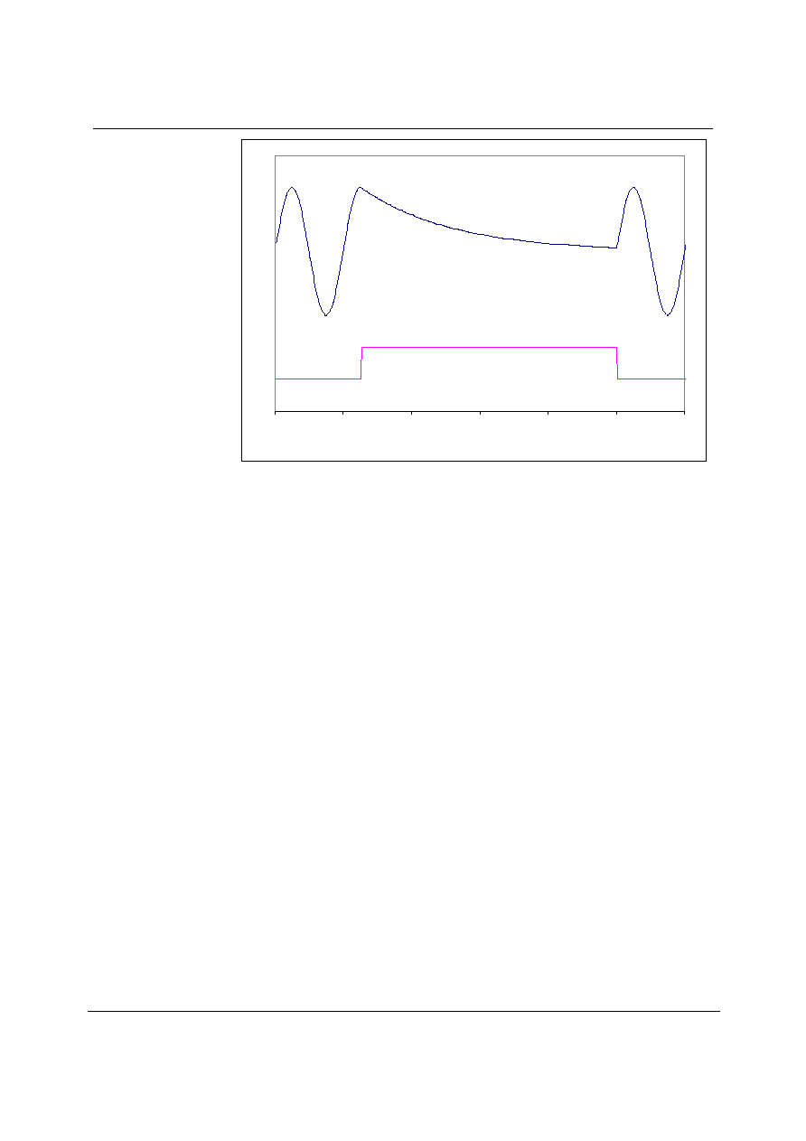
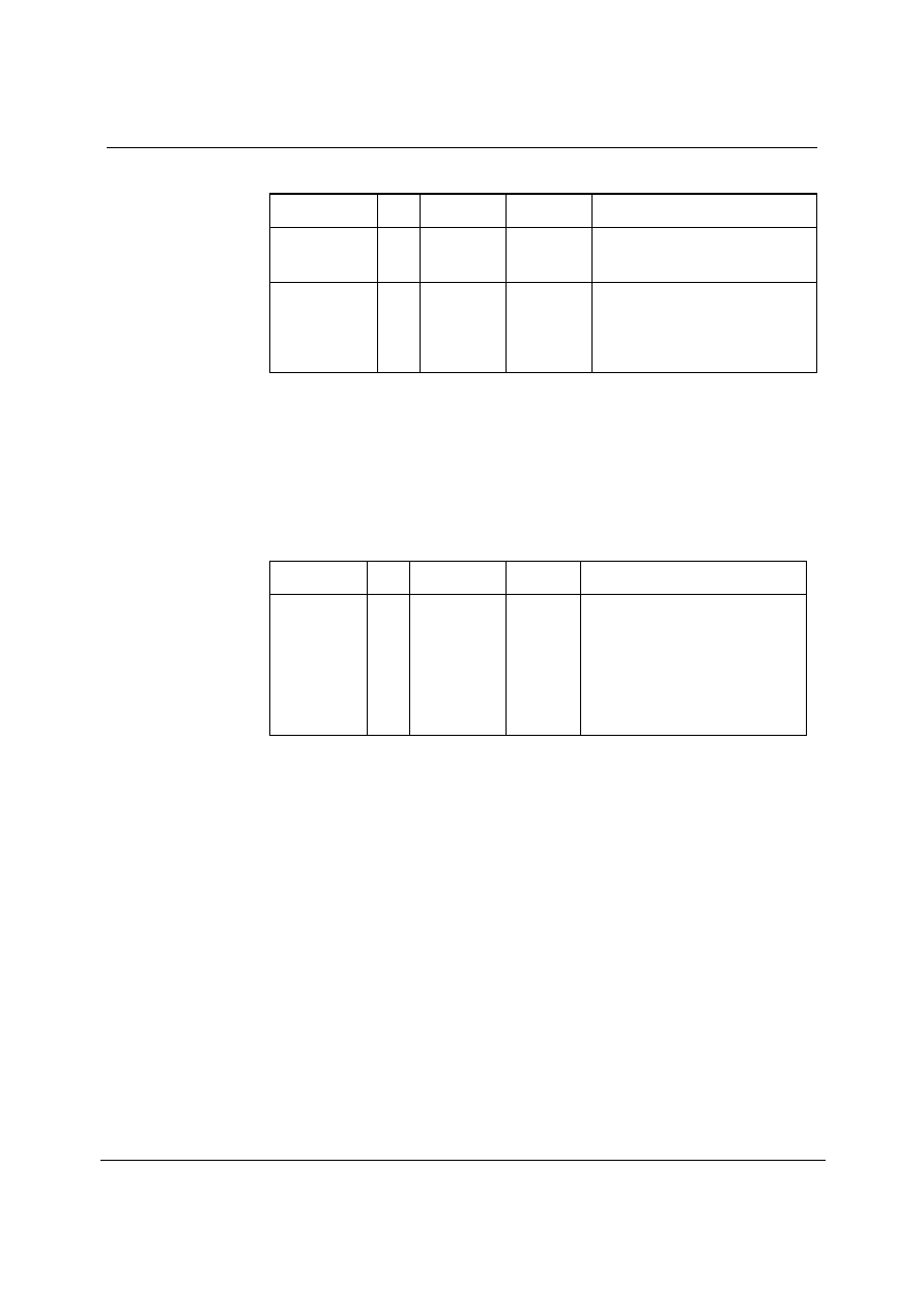
Figure 21 Application and Release of Soft Mute
Figure 21 shows the application and release of DMUTE whilst a full amplitude sinusoid is being
played at 48kHz sampling rate. When DMUTE (lower trace) is asserted, the output (upper trace)
begins to decay exponentially from the DC level of the last input sample. The output will decay
towards V
MID
with a time constant of approximately 64 input samples. If DMUTE is applied to both
channels for 1024 or more input samples the DAC will be muted if IZD is set. When DMUTE is de-
asserted, the output will restart immediately from the current input sample.
Note that all other means of muting the DAC: setting the PL[3:0] bits to 0, setting the PDWN bit or
setting attenuation to 0 will cause much more abrupt muting of the output.
-2.5
-2
-1.5
-1
-0.5
0
0.5
1
1.5
0
0.001
0.002
0.003
0.004
0.005
0.006
Time(s)
Product Preview
WM8778
w
PP Rev 1.7 June 2004
27
ADC MUTE
Each ADC channel also has an individual mute control bit, which mutes the input to the ADC PGA.
By setting the LRBOTH bit (reg22, bit 8) both channels can be muted simultaneously.
REGISTER ADDRESS
BIT
LABEL
DEFAULT
DESCRIPTION
R21 (15h)
0010101
ADC Mute Left
7
MUTELA
0
ADC Mute Select
0 : Normal Operation
1: mute ADC left
R21 (15h)
0001111
ADC Mute Right
6
MUTERA
0
ADC Mute Select
0 : Normal Operation
1: mute ADC right
DE-EMPHASIS MODE
The De-emphasis filter for the DAC is enabled under the control of DEEMP.
REGISTER ADDRESS
BIT
LABEL
DEFAULT
DESCRIPTION
R9 (09h)
0001001
DAC De-emphasis
Control
0
DEEMPH
0
De-emphasis Mode Select:
0 : Normal Mode
1: De-emphasis Mode
Refer to Figure 32, Figure 33, Figure 34, Figure 35, Figure 36 and Figure 37 for details of the De-
Emphasis modes at different sample rates.
POWERDOWN MODE AND ADC/DAC DISABLE
Setting the PDWN register bit immediately powers down the WM8778, including the references,
overriding all other powerdown control bits. All trace of the previous input samples is removed, but all
control register settings are preserved. When PDWN is cleared, the digital filters will be re-initialised.
It is recommended that the buffer, ADC and DAC are powered down before setting PDWN.
REGISTER ADDRESS
BIT
LABEL
DEFAULT
DESCRIPTION
R13 (0Dh)
0001101
Powerdown Control
0
PDWN
0
Power Down Mode Select:
0 : Normal Mode
1: Power Down Mode
The ADC and DAC may also be powered down by setting the ADCPD and DACPD disable bits.
Setting ADCPD will disable the ADC and select a low power mode. The ADC digital filters will be
reset and will reinitialise when ADCPD is reset. The DAC has a separate disable DACPD. Setting
DACPD will disable the DAC, mixer and output PGAs. Resetting DACPD will reinitialise the digital
filters.
REGISTER ADDRESS
BIT
LABEL
DEFAULT
DESCRIPTION
1
ADCPD
0
ADC Powerdown:
0 : Normal Mode
1: Power Down Mode
R13 (0Dh)
0001101
Powerdown Control
2
DACPD
0
DAC Powerdown:
0 : Normal Mode
1: Power Down Mode
The analogue audio inputs and outputs can also be individually powered down by setting the relevant
bits in the powerdown register.
WM8778
Product Preview
w
PP Rev 1.7 June 2004
28
REGISTER ADDRESS
BIT
LABEL
DEFAULT
DESCRIPTION
R13 (0Dh)
0001101
Powerdown Control
6
AINPD
0
Analogue Input PGA Disable:
0 : Normal Mode
1: Power Down Mode
DIGITAL ATTENUATOR CONTROL MODE
Setting the ATC register bit causes the left channel attenuation settings to be applied to both left and
right channel DACs from the next audio input sample. No update to the attenuation registers is
required for ATC to take effect.
REGISTER ADDRESS
BIT
LABEL
DEFAULT
DESCRIPTION
R7 (07h)
0000111
DAC Channel Control
1
ATC
0
Attenuator Control Mode:
0 : Right channel use Right
attenuation
1: Right Channel use Left
Attenuation
INFINITE ZERO DETECT ENABLE
Setting the IZD register bit will enable the internal infinite zero detect function:
REGISTER ADDRESS
BIT
LABEL
DEFAULT
DESCRIPTION
R7 (07h)
0000111
DAC Channel Control
2
IZD
0
Infinite Zero Mute Enable
0 : disable infinite zero mute
1: enable infinite zero Mute
With IZD enabled, applying 1024 consecutive zero input samples to the DAC will cause both DAC
outputs to be muted. Mute will be removed as soon as any channel receives a non-zero input.
DAC OUTPUT CONTROL
The DAC output control word determines how the left and right inputs to the audio Interface are
applied to the left and right DACs:
REGISTER ADDRESS
BIT
LABEL
DEFAULT
DESCRIPTION
PL[3:0]
Left
Output
Right
Output
0000
Mute
Mute
0001
Left
Mute
0010
Right
Mute
0011
(L+R)/2
Mute
0100
Mute
Left
0101
Left
Left
0110
Right
Left
0111
(L+R)/2
Left
1000
Mute
Right
1001
Left
Right
1010
Right
Right
1011
(L+R)/2
Right
1100
Mute
(L+R)/2
1101
Left
(L+R)/2
1110
Right
(L+R)/2
R7 (07h)
0000111
DAC Control
7:4
PL[3:0]
1001
1111
(L+R)/2
(L+R)/2
Product Preview
WM8778
w
PP Rev 1.7 June 2004
29
DAC DIGITAL VOLUME CONTROL
The DAC volume may also be adjusted in the digital domain using independent digital attenuation
control registers
REGISTER
ADDRESS
BIT
LABEL
DEFAULT
DESCRIPTION
7:0
LDA[7:0]
11111111
(0dB)
Digital Attenuation data for Left channel DACL in 0.5dB steps. See
Table 13
R3 (03h)
0000011
Digital
Attenuation
DACL
8
UPDATED
Not latched
Controls simultaneous update of Attenuation Latches
0: Store LDA in intermediate latch (no change to output)
1: Store LDA and update attenuation on both channels
7:0
RDA[6:0]
11111111
(0dB)
Digital Attenuation data for Right channel DACR in 0.5dB steps. See
Table 13
R4 (04h)
0000100
Digital
Attenuation
DACR
8
UPDATED
Not latched
Controls simultaneous update of Attenuation Latches
0: Store RDA in intermediate latch (no change to output)
1: Store RDA and update attenuation on both channels.
7:0
MASTDA[7:0]
11111111
(0dB)
Digital Attenuation data for DAC channels in 0.5dB steps. See Table
13
R5 (05h)
0000101
Master
Digital
Attenuation
(both channels)
8
UPDATED
Not latched
Controls simultaneous update of Attenuation Latches
0: Store gain in intermediate latch (no change to output)
1: Store gain and update attenuation on channels.
L/RDA[7:0]
ATTENUATION LEVEL
00(hex)
-
dB (mute)
01(hex)
-127dB
:
:
:
:
:
:
FE(hex)
-0.5dB
FF(hex)
0dB
Table 13 Digital Volume Control Attenuation Levels
The digital volume control also incorporates a zero cross detect circuit which detects a transition
through the zero point before updating the digital volume control with the new volume. This is
enabled by control bit DZCEN.
REGISTER ADDRESS
BIT
LABEL
DEFAULT
DESCRIPTION
R7 (07h)
0000111
DAC Control
0
DZCEN
0
DAC Digital Volume Zero Cross
Enable:
0: Zero cross detect disabled
1: Zero cross detect enabled
DAC OUTPUT PHASE
The DAC Phase control word determines whether the output of the DAC is non-inverted or inverted
REGISTER ADDRESS
BIT
LABEL
DEFAULT
DESCRIPTION
Bit
DAC
Phase
0
DACL
1 = invert
R6 (06h)
0000110
DAC Phase
1:0
PHASE
[1:0]
00
1
DACR
1 = invert

WM8778
Product Preview
w
PP Rev 1.7 June 2004
30
ADC GAIN CONTROL
The ADC has an analogue input PGA and digital gain control for each stereo channel. Both the
analogue and digital gains are adjusted by the same register, LAG for the left and RAG for the right.
The analogue PGA has a range of +24dB to -21dB in 0.5dB steps. The digital gain control allows
further attenuation (after the ADC) from -21.5dB to -103dB in 0.5dB steps. Table 14 shows how the
register maps the analogue and digital gains.
LAG/RAG[7:0]
ATTENUATION
LEVEL (AT
OUTPUT)
ANALOGUE PGA
DIGITAL
ATTENUATION
00(hex)
-
dB (mute)
-21dB
Digital mute
01(hex)
-103dB
-21dB
-82dB
:
:
:
:
A4(hex)
-21.5dB
-21dB
-0.5dB
A5(hex)
-21dB
-21dB
0dB
:
:
:
:
CF(hex)
0dB
0dB
0dB
:
:
:
:
FE(hex)
+23.5dB
+23.5dB
0dB
FF(hex)
+24dB
+24dB
0dB
Table 14 Analogue and Digital Gain Mapping for ADC
In addition a zero cross detect circuit is provided for the input PGA. When ZCLA/ZCRA is set with a
write, the gain will update only when the input signal approaches zero (midrail). This minimises
audible clicks and `zipper' noise as the gain values change. A timeout clock is also provided which
will generate an update after a minimum of 131072 master clocks (= ~10.5ms with a master clock of
12.288MHz). The timeout clock may be disabled by setting TOD.
REGISTER ADDRESS
BIT
LABEL
DEFAULT
DESCRIPTION
R7 (07h)
0000111
Timeout Clock Disable
3
TOD
0
Analogue PGA Zero Cross Detect
Timeout Disable
0 : Timeout enabled
1: Timeout disabled
Product Preview
WM8778
w
PP Rev 1.7 June 2004
31
Left and right inputs may also be independently muted. The LRBOTH control bit allows the user to
write the same attenuation value to both left and right volume control registers, saving on software
writes. The ADC volume and mute also applies to the bypass signal path.
REGISTER
ADDRESS
BIT
LABEL
DEFAULT
DESCRIPTION
7:0
LAG[7:0]
11001111
(0dB)
Attenuation Data for Left Channel ADC Gain in 0.5dB steps. See
Table 14.
R14 (0Eh)
0001110
Attenuation
ADCL
8
ZCLA
0
Left Channel ADC Zero Cross Enable:
0: Zero cross disabled
1: Zero cross enabled
7:0
RAG[7:0]
11001111
(0dB)
Attenuation data for right channel ADC gain in 0.5dB steps. See
Table 14.
R15 (0Fh)
0001111
Attenuation
ADCR
8
ZCRA
0
Right Channel ADC Zero Cross Enable:
0: Zero cross disabled
1: Zero cross enabled
6
MUTERA
0
Mute for Right Channel ADC
0: Mute Off
1: Mute on
7
MUTELA
0
Mute for Left Channel ADC
0: Mute Off
1: Mute on
R21 (15h)
0010101
ADC Input Mux
8
LRBOTH
0
Right Channel Input PGA Controlled by Left Channel Register
0 : Right channel uses RAG and MUTERA.
1 : Right channel uses LAG and MUTELA.
ADC HIGHPASS FILTER DISABLE
The ADC digital filters contain a digital high pass filter. This defaults to enabled and can be disabled
using software control bit ADCHPD.
REGISTER ADDRESS
BIT
LABEL
DEFAULT
DESCRIPTION
R11 (0Bh)
0001011
ADC Control
8
ADCHPD
0
ADC High Pass Filter Disable:
0: High pass filter enabled
1: High pass filter disabled
WM8778
Product Preview
w
PP Rev 1.7 June 2004
32
LIMITER / AUTOMATIC LEVEL CONTROL (ALC)
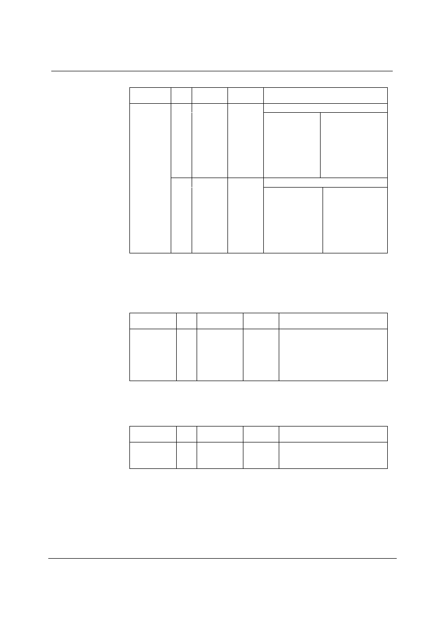
The WM8778 has an automatic pga gain control circuit, which can function as a peak limiter or as an
automatic level control (ALC). In peak limiter mode, a digital peak detector detects when the input
signal goes above a predefined level and will ramp the pga gain down to prevent the signal becoming
too large for the input range of the ADC. When the signal returns to a level below the threshold, the
pga gain is slowly returned to its starting level. The peak limiter cannot increase the pga gain above
its static level.
Figure 22 Limiter Operation
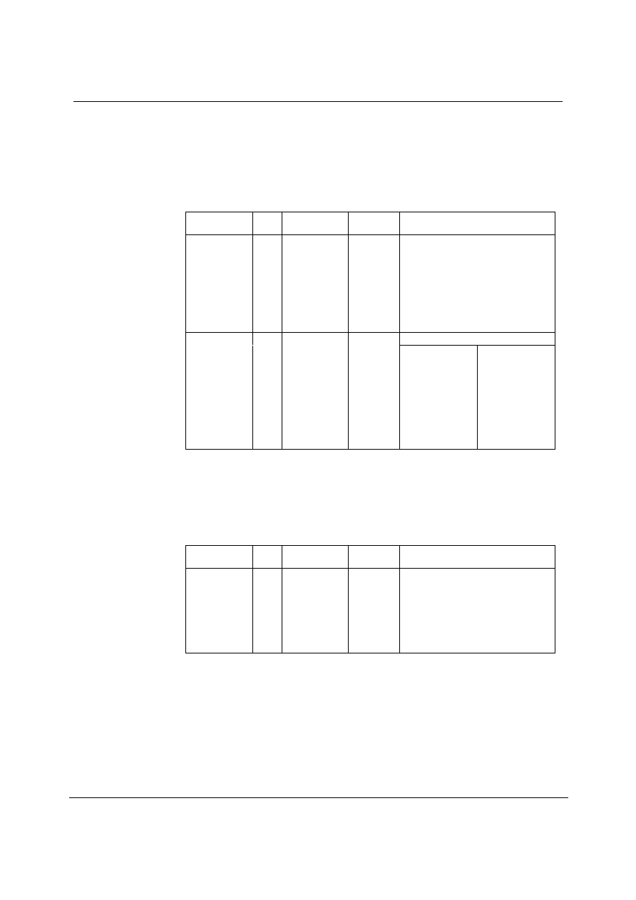
In ALC mode, the circuit aims to keep a constant recording volume irrespective of the input signal
level. This is achieved by continuously adjusting the PGA gain so that the signal level at the ADC
input remains constant. A digital peak detector monitors the ADC output and changes the PGA gain
if necessary.
Figure 23 ALC Operation
hold
time
decay
time
attack
time
input
signal
signal
after
ALC
PGA
gain
ALC
target
level
input
signal
signal
after
PGA
PGA
gain
Limiter
threshold
attack
time
decay
time
Product Preview
WM8778
w
PP Rev 1.7 June 2004
33
The gain control circuit is enabled by setting the LCEN control bit. The user can select between
Limiter mode and three different ALC modes using the LCSEL control bits.
REGISTER
ADDRESS
BIT
LABEL
DEFAULT
DESCRIPTION
R17 (11h)
0010001
ALC Control 2
8
LCEN
0
Enable the PGA Gain Control Circuit.
0 = Disabled
1 = Enabled
R16 (10h)
0010000
ALC Control 1
8:7
LCSEL
00
LC Function Select
00 = Limiter
01 = ALC Right channel only
10 = ALC Left channel only
11 = ALC Stereo
The limiter function only operates in stereo, which means that the peak detector takes the maximum
of left and right channel peak values, and any new gain setting is applied to both left and right PGAs,
so that the stereo image is preserved. However, the ALC function can also be enabled on one
channel only. In this case, only one PGA is controlled by the ALC mechanism, while the other
channel runs independently with its PGA gain set through the control register.
When enabled, the threshold for the limiter or target level for the ALC is programmed using the LCT
control bits. This allows the threshold/target level to be programmed between -1dB and -16dB in 1dB
steps. Note that for the ALC, target levels of -1dB and -2dB give a threshold of -3dB. This is
because the ALC can give erroneous operation if the target level is set too high.
REGISTER
ADDRESS
BIT
LABEL
DEFAULT
DESCRIPTION
R16 (10h)
0010000
ALC Control 1
3:0
LCT[3:0]
1011
(-5dB)
Limiter Threshold/ALC Target Level in
1dB Steps:
0000: -16dB FS
0001: -15dB FS
...
1101: -3dB FS
1110: -2dB FS
1111: -1dB FS
ATTACK AND DECAY TIMES
The limiter and ALC have different attack and decay times which determine their operation. However,
the attack and decay times are defined slightly differently for the limiter and for the ALC. DCY and
ATK control the decay and attack times, respectively.
Decay time (Gain Ramp-Up). When in ALC mode, this is defined as the time that it takes for the
PGA gain to ramp up across 90% of its range (e.g. from ≠21dB up to +20 dB). When in limiter mode,
it is defined as the time it takes for the gain to ramp up by 6dB.
The decay time can be programmed in power-of-two (2
n
) steps. For the ALC this gives times from
33.6ms, 67.2ms, 134.4ms etc. to 34.41s. For the limiter this gives times from 1.2ms, 2.4ms etc., up
to 1.2288s.
Attack time (Gain Ramp-Down) When in ALC mode, this is defined as the time that it takes for the
PGA gain to ramp down across 90% of its range (e.g. from +20dB down to -21dB gain). When in
limiter mode, it is defined as the time it takes for the gain to ramp down by 6dB.
The attack time can be programmed in power-of-two (2
n
) steps, from 8.4ms, 16.8ms, 33.6ms etc. to
8.6s for the ALC and from 250us, 500us, etc. up to 256ms.
The time it takes for the recording level to return to its target value or static gain value therefore
depends on both the attack/decay time and on the gain adjustment required. If the gain adjustment is
small, it will be shorter than the attack/decay time.
WM8778
Product Preview
w
PP Rev 1.7 June 2004
34
REGISTER
ADDRESS
BIT
LABEL
DEFAULT
DESCRIPTION
LC Attack (Gain Ramp-down) Time
3:0
ATK[3:0]
0010
ALC mode
0000: 8.4ms
0001: 16.8ms
0010: 33.6ms...
(time doubles with
every step)
1010 or higher:
8.6s
Limiter Mode
0000: 250us
0001: 500us... 0010:
1ms
(time doubles with
every step)
1010 or higher: 256ms
LC Decay (Gain Ramp-up) Time
R18 (12h)
0010010
ALC
Control 3
7:4
DCY [3:0]
0011
ALC mode
0000: 33.5ms
0001: 67.2ms
0010: 134.4ms
....(time doubles for
every step)
1010 or higher:
34.3 ms
Limiter mode
0000: 1.2ms
0001: 2.4ms
0010: 4.8ms ....(time
doubles for every
step)
1010 or higher:
1.2288s
TRANSIENT WINDOW (LIMITER ONLY)
To prevent the limiter responding to to short duration high ampitude signals (such as hand-claps in a
live performance), the limiter has a programmable transient window preventing it responding to
signals above the threshold until their duration exceeds the window period. The Transient window is
set in register TRANWIN.
REGISTER
ADDRESS
BIT
LABEL
DEFAULT
DESCRIPTION
R20 (14h)
0010100
Limiter Control
6:4
TRANWIN
[2:0]
010
Length of Transient Window:
000: 0us (disabled)
001: 62.5us
010: 125us
.....
111: 4ms
ZERO CROSS
The PGA has a zero cross detector to prevent gain changes introducing noise to the signal. In ALC
mode the register bit ALCZC allows this to be turned off if desired.
REGISTER
ADDRESS
BIT
LABEL
DEFAULT
DESCRIPTION
R17 (11h)
0010001
ALC Control 2
7
ALCZC
0
(disabled)
PGA Zero Cross Enable:
0 : disabled
1: enabled
Product Preview
WM8778
w
PP Rev 1.7 June 2004
35
MAXIMUM GAIN (ALC ONLY) AND MAXIMUM ATTENUATION
To prevent low level signals being amplified too much by the ALC, the MAXGAIN register sets the
upper limit for the gain. This prevents low level noise being over-amplified. The MAXGAIN register
has no effect on the limiter operation.
The
register has different operation for the limiter and for the ALC. For the limiter it defines the maximum
attenuation below the static (user programmed) gain. For the ALC, it defines the lower limit for the
gain.
REGISTER
ADDRESS
BIT
LABEL
DEFAULT
DESCRIPTION
R16 (10h)
0010000
ALC Control 1
6:4
MAXGAIN
111
(+24dB)
Set Maximum Gain for the PGA (ALC
only):
111 : +24dB
110 : +20dB
.....(-4dB steps)
010 : +4dB
001 : 0dB
000 : 0dB
Maximum Attenuation of PGA
R20 (14h)
0010100
Limiter Control
3:0
MAXATTEN
0110
Limiter
(attenuation
below static)
0011 or lower
: -3dB
0100: -4dB
.... (-1dB steps)
1100 or higher
: -12dB
ALC (lower PGA
gain limit)
1010 or lower
: -1dB
1011 : -5dB
..... (-4dB steps)
1110 : -17dB
1111 : -21dB
HOLD TIME (ALC ONLY)
The ALC also has a hold time, which is the time delay between the peak level detected being below
target and the PGA gain beginning to ramp up. It can be programmed in power-of-two (2
n
) steps, e.g.
2.67ms, 5.33ms, 10.67ms etc. up to 43.7ms. Alternatively, the hold time can also be set to zero. The
hold time only applies to gain ramp-up, there is no delay before ramping the gain down when the
signal level is above target.
REGISTER
ADDRESS
BIT
LABEL
DEFAULT
DESCRIPTION
R17 (11h)
0010001
ALC Control 2
3:0
HLD[3:0]
0000
ALC Hold Time Before Gain is
Increased:
0000: 0ms
0001: 2.67ms
0010: 5.33ms
... (time doubles with every step)
1111: 43.691s

WM8778
Product Preview
w
PP Rev 1.7 June 2004
36
OVERLOAD DETECTOR (ALC ONLY)
To prevent clipping when a large signal occurs just after a period of quiet, the ALC circuit includes an
overload detector. If the ADC input signal exceeds 87.5% of full scale (≠1.16dB), the PGA gain is
ramped down at the maximum attack rate (as when ATK = 0000), until the signal level falls below
87.5% of full scale. This function is automatically enabled whenever the ALC is enabled.
(Note: If ATK = 0000, then the overload detector makes no difference to the operation of the ALC. It
is designed to prevent clipping when long attack times are used).
NOISE GATE (ALC ONLY)
When the signal is very quiet and consists mainly of noise, the ALC function may cause "noise
pumping", i.e. loud hissing noise during silence periods. The WM8778 has a noise gate function that
prevents noise pumping by comparing the signal level at the AINL1/2/3/4/5 and/or AINR1/2/3/4/5 pins
against a noise gate threshold, NGTH. The noise gate cuts in when:
∑
Signal level at ADC [dB] < NGTH [dB] + PGA gain [dB] + Mic Boost gain [dB]
This is equivalent to:
∑
Signal level at input pin [dB] < NGTH [dB]
When the noise gate is triggered, the PGA gain is held constant (preventing it from ramping up as it
would normally when the signal is quiet).
The table below summarises the noise gate control register. The NGTH control bits set the noise
gate threshold with respect to the ADC full-scale range. The threshold is adjusted in 6dB steps.
Levels at the extremes of the range may cause inappropriate operation, so care should be taken with
set≠up of the function. Note that the noise gate only works in conjunction with the ALC function, and
always operates on the same channel(s) as the ALC (left, right, both, or none).
REGISTER
ADDRESS
BIT
LABEL
DEFAULT
DESCRIPTION
0
NGAT
0
Noise Gate Function Enable:
1 = enable
0 = disable
R19 (13h)
0010011
Noise Gate
Control
4:2
NGTH[2:0]
000
Noise Gate Threshold (with respect to
ADC output level):
000: -78dBFS
001: -72dBfs
... 6 dB steps
110: -42dBFS
111: -36dBFS
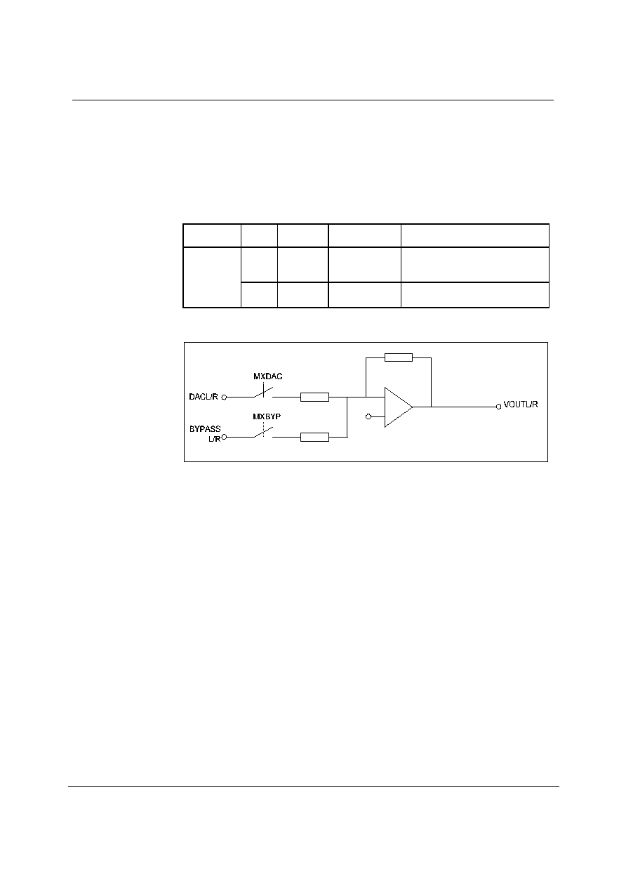
Product Preview
WM8778
w
PP Rev 1.7 June 2004
37
OUTPUT SELECT AND ENABLE CONTROL
Register bits MXDAC and MXBYP controls the output selection. The output select block consists of a
summing stage and an input select switch for each input allowing each signal to be output
individually or summed with other signals and output on the analogue output. The default for the
output is DAC playback only. VOUT may be selected to output DAC playback, analogue bypass or a
sum of the two using the output select controls MXDAC and MXBYP.
The output mixer is powered down when PDWN is set. The bypass path is automatically deselected
when AINPD is set.
REGISTER
ADDRESS
BIT
LABEL
DEFAULT
DESCRIPTION
0
MXDAC
1
(DAC playback)
VOUT Output Select DAC (see
Figure 24)
R22 (16h)
0010110
Output Mux
2
MXBYP
0
(not selected)
VOUT Output Select Bypass Path.
Figure 24 MX[2:0] Output Select
SOFTWARE REGISTER RESET
Writing any value to register 0010111 will cause a register reset, resetting all register bits to their
default values.

WM8778
Product Preview
w
PP Rev 1.7 June 2004
38
REGISTER MAP
The complete register map is shown below. The detailed description can be found in the relevant text of the device description. The
WM8778 can be configured using the Control Interface. All unused bits should be set to `0'.
REGISTER B
15
B
14
B
13
B
12
B
11
B
10
B
9
B8
B7
B6
B5
B4
B3
B2
B1
B0
DEFAULT
(HEX)
R3 (03h)
0
0
0
0
0
1
1 UPDATED
LDA[7:0]
0FF
R4 (04h)
0
0
0
0
1
0
0 UPDATED
RDA[7:0]
0FF
R5 (05h)
0
0
0
0
1
0
1 UPDATED
MASTDA[7:0]
0FF
R6 (06h)
0
0
0
0
1
1
0
0
0
0
0
0
0
0
PHASE[1:0]
000
R7 (07h)
0
0
0
0
1
1
1
0
PL[3:0]
TOD
IZD
ATC
DZCEN
090
R8 (08h)
0
0
0
1
0
0
0
0
0
0
0
0
0
0
0
DMUTE
000
R9 (09h)
0
0
0
1
0
0
1
0
0
0
0
0
0
DZFM [1:0]
DEEMPH
000
R10 (0Ah) 0 0
0
1
0
1
0
0
0
0
DACWL[1:0]
DACBCP DACLRP
DACFMT[1:0]
022
R11 (0Bh) 0 0
0
1
0
1
1
ADCHPD
0
ADCMCLK
ADCWL[1:0]
ADCBCP ADCLRP
ADCFMT[1:0]
022
R12 (0Ch) 0 0
0
1
1
0
0
ADCMS
DACMS
DACRATE[2:0]
ADCOSR
ADCRATE[2:0]
022
R13 (ODh) 0 0
0
1
1
0
1
0
0
AINPD
0
0
0
DACPD ADCPD
PDWN
008
R14 (0Eh) 0 0
0
1
1
1
0
ZCLA
LAG[7:0]
0CF
R15 (0Fh)
0
0
0
1
1
1
1
ZCRA
RAG[7:0]
0CF
R16 (10h)
0
0
1
0
0
0
0
LCSEL[1:0]
MAXGAIN[2:0]
LCT[3:0]
07B
R17 (11h)
0
0
1
0
0
0
1
LCEN
ALCZC
0
0
0
HLD[3:0]
000
R18 (12h)
0
0
1
0
0
1
0
0
DCY[3:0]
ATK[3:0]
032
R19 (13h)
0
0
1
0
0
1
1
0
0
0
0
NGTH[2:0]
0
NGAT
000
R20 (14h)
0
0
1
0
1
0
0
0
0
TRANWIN[2:0]
MAXATTEN[3:0]
0A6
R21 (15h)
0
0
1
0
1
0
1
LRBOTH
MUTELA
MUTERA
0
0
001
R22 (16h)
0
0
1
0
1
1
0
0
0
0
MXBYP
0
MXDAC
001
R23 (17h)
0
0
1
0
1
1
1
SOFTWARE RESET
not reset
Product Preview
WM8778
w
PP Rev 1.7 June 2004
39
REGISTER
ADDRESS
BIT
LABEL
DEFAULT
DESCRIPTION
7:0
LDA[7:0]
11111111
(0dB)
Digital Attenuation Data for Left Channel DACL in 0.5dB Steps.
R3 (03h)
0000011
Digital
Attenuation
DACL
8
UPDATED
Not latched
Controls Simultaneous Update of all Attenuation Latches
0: Store LDA1 in intermediate latch (no change to output)
1: Store LDA1 and update attenuation on all channels
7:0
RDA[6:0]
11111111
(0dB)
Digital Attenuation Data for Right Channel DACR in 0.5dB Steps.
R4 (04h)
0000100
Digital
Attenuation
DACR
8
UPDATED
Not latched
Controls Simultaneous Update of all Attenuation Latches
0: Store RDA1 in intermediate latch (no change to output)
1: Store RDA1 and update attenuation on all channels.
7:0
MASTDA[7:0]
11111111
(0dB)
Digital Attenuation Data for all DAC Channels in 0.5dB Steps.
R5 (05h)
0000101
Master
Digital
Attenuation
(All Channels)
8
UPDATED
Not latched
Controls Simultaneous Update of all Attenuation Latches
0: Store gain in intermediate latch (no change to output)
1: Store gain and update attenuation on all channels.
R6 (06h)
0000110
Phase Swaps
1:0
PHASE
00
Controls Phase of DAC Outputs (LEFT, RIGHT Channel)
0: Sets non inverted output phase
1: inverts phase of DAC output
0
DZCEN
0
DAC Digital Volume Zero Cross Enable:
0: Zero Cross detect disabled
1: Zero Cross detect enabled
1
ATC
0
Attenuator Control:
0: All DACs use attenuations as programmed.
1: Right DAC uses left DAC attenuations
2
IZD
0
Infinite Zero Detection Circuit Control and Automute Control
0: Infinite zero detect automute disabled
1: Infinite zero detect automute enabled
3
TOD
0
DAC and ADC Analogue Zero Cross Detect Timeout Disable
0 : Timeout enabled
1: Timeout disabled
DAC Output Control
PL[3:0]
Left
Output
Right
Output
PL[3:0]
Left
Output
Right
Output
0000
Mute
Mute
1000
Mute
Right
0001
Left
Mute
1001
Left
Right
0010
Right
Mute
1010
Right
Right
0011
(L+R)/2
Mute
1011
(L+R)/2
Right
0100
Mute
Left
1100
Mute
(L+R)/2
0101
Left
Left
1101
Left
(L+R)/2
0110
Right
Left
1110
Right
(L+R)/2
R7 (07h)
0000111
DAC Control
7:4
PL[3:0]
1001
0111
(L+R)/2
Left
1111
(L+R)/2
(L+R)/2
R8 (08h)
0001000
DAC Mute
0
DMUTE
0
DAC Channel Soft Mute Enables:
0: mute disabled
1: mute enabled
WM8778
Product Preview
w
PP Rev 1.7 June 2004
40
REGISTER
ADDRESS
BIT
LABEL
DEFAULT
DESCRIPTION
0
DEEMP
0
De-emphasis Mode Select:
0 : Normal Mode
1: De-emphasis Mode
DZFM
ZFLAG1
ZFLAG2
R9 (09h)
0001001
DAC Control
2:1
DZFM
00
00
01
10
11
disabled
left channels zero
both channels zero
either channel zero
disabled
right channels zero
both channels zero
either channel zero
1:0
DACFMT[1:0]
10
DAC Interface Format Select:
00: right justified mode
01: left justified mode
10: I
2
S mode
11: DSP mode
DACLRC Polarity or DSP Early/Late Mode Select
2
DACLRP
0
Left Justified / Right Justified /
I
2
S:
0: Standard DACLRC Polarity
1: Inverted DACLRC Polarity
DSP Mode:
0: Early Mode
1: Late Mode
3
DACBCP
0
DAC BITCLK Polarity:
0: Normal ≠ DIN and DACLRC sampled on rising edge of
DACBCLK.
1: Inverted - DIN and DACLRC sampled on falling edge of
DACBCLK.
R10 (0Ah)
0001010
DAC Interface
Control
5:4
DACWL[1:0]
10
DAC Input Word Length:
00: 16-bit Mode
01: 20-bit Mode
10: 24-bit Mode
11: 32-bit Mode (not supported in right justified mode)
1:0
ADCFMT[1:0]
10
ADC Interface Format Select:
00: right justified mode
01: left justified mode
10: I
2
S mode
11: DSP mode
ADCLRC Polarity or DSP Early/Late mode select
2
ADCLRP
0
Left Justified / Right Justified /
I
2
S:
0: Standard ADCLRC Polarity
1: Inverted ADCLRC Polarity
DSP Mode:
0: Early Mode
1: Late Mode
3
ADCBCP
0
ADC BITCLK Polarity:
0: Normal - ADCLRC sampled on rising edge of
ADCBCLK; DOUT changes on falling edge of ADCBCLK.
1: Inverted - ADCLRC sampled on falling edge of
ADCBCLK; DOUT changes on rising edge of ADCBCLK.
5:4
ADCWL[1:0]
10
ADC Input Word Length:
00: 16-bit Mode
01: 20-bit Mode
10: 24-bit Mode
11: 32-bit Mode (not supported in right justified mode)
R11 (0Bh)
0001011
ADC Interface
Control
6
ADCMCLK
0
ADCMCLK Polarity:
0: non-inverted
1: inverted
Product Preview
WM8778
w
PP Rev 1.7 June 2004
41
REGISTER
ADDRESS
BIT
LABEL
DEFAULT
DESCRIPTION
8
ADCHPD
0
ADC Highpass Filter Disable:
0: Highpass Filter enabled
1: Highpass Filter disabled
2:0
ADCRATE[2:0]
010
Master Mode ADCMCLK:ADCLRC Ratio Select:
010: 256fs
011: 384fs
100: 512fs
101: 768fs
3
ADCOSR
0
ADC Oversample Rate Select:
0: 128x oversampling
1: 64x oversapmling
6:4
DACRATE[2:0]
010
Master Mode DACMCLK:DACLRC Ratio Select:
000: 128fs
001: 192fs
010: 256fs
011: 384fs
100: 512fs
101: 768fs
7
DACMS
0
DAC Maser/Slave Interface Mode Select:
0: Slave Mode ≠ DACLRC and DACBCLK are inputs
1: Master Mode ≠DACLRC and DACBCLK are outputs
R12 (0Ch)
0001100
Master Mode
Control
8
ADCMS
0
ADC Maser/Slave Interface Mode Select:
0: Slave Mode ≠ ADCLRC and ADCBCLK are inputs
1: Master Mode ≠ ADCLRC and ADCBCLK are outputs
0
PDWN
0
Chip Powerdown Control (works in tandem with ADCPD and
DACPD):
0: All circuits running, outputs are active
1: All circuits in power save mode, outputs muted
1
ADCPD
0
ADC Powerdown:
0: ADC enabled
1: ADC disabled
2
DACPD
0
DAC Powerdown:
0: DAC enabled
1: DAC disabled
R13 (0Dh)
0001101
PWR Down
Control
6
AINPD
0
AINPD Powerdown:
0: ANALOGUE INPUT enabled
1: ANALOGUE INPUT disabled
7:0
LAG[7:0]
11001111
(0dB)
Attenuation Data for Left Channel ADC Gain in 0.5dB Steps:
00000000 : digital mute
00000001 : -103dB
...........
11001111 : 0dB
............
11111110 : +23.5dB
11111111 : +24dB
R14 (0Eh)
0001110
Attenuation
ADCL
8
ZCLA
0
Left ADC Zero Cross Enable:
0: Zero cross disabled
1: Zero cross enabled

WM8778
Product Preview
w
PP Rev 1.7 June 2004
42
REGISTER
ADDRESS
BIT
LABEL
DEFAULT
DESCRIPTION
7:0
RAG[7:0]
11001111
(0dB)
Attenuation Data for Right Channel ADC Gain in 0.5dB Steps:
00000000 : digital mute
00000001 : -103dB
...........
11001111 : 0dB
............
11111110 : +23.5dB
11111111 : +24dB
R15 (0Fh)
0001111
Attenuation
ADCR
8
ZCRA
0
Right ADC Zero Cross Enable:
0: Zero cross disabled
1: Zero cross enabled
3:0
LCT[3:0]
1011
(-5dB)
Limiter Threshold/ALC Target Level in 1dB Steps:
0000: -16dB FS
0001: -15dB FS
...
1101: -3dB FS
1110: -2dB FS
1111: -1dB FS
6:4
MAXGAIN[2:0]
111 (+24dB)
Set Maximum Gain of PGA:
111 : +24dB
110 : +20dB
....(-4dB steps)
010 : +4dB
001 : 0dB
000 : 0dB
R16 (10h)
0010000
ALC Control 1
8:7
LCSEL[1:0]
00
(Limiter)
ALC/Limiter Function Select:
00 = Limiter
01 = ALC Right channel only
10 = ALC Left channel only
11 = ALC Stereo (PGA registers unused)
3:0
HLD[3:0]
0000
(OFF)
ALC Hold Time Before Gain is Increased:
0000: OFF
0001: 2.67ms
0010: 5.33ms
... (time doubles with every step)
1111: 43.691s
7
ALCZC
0 (zero cross
off)
ALC Uses Zero Cross Detection Circuit.
R17 (11h)
0010001
ALC Control 2
8
LCEN
0
Enable Gain Control Circuit.
0 = Disable
1 = Enable
Product Preview
WM8778
w
PP Rev 1.7 June 2004
43
REGISTER
ADDRESS
BIT
LABEL
DEFAULT
DESCRIPTION
ALC/Limiter Attack (gain ramp-down) Time
3:0
ATK[3:0]
0010
(33ms/1ms)
ALC Mode
0000: 8.4ms
0001: 16.8ms
0010: 33.6ms...
(time doubles with every step)
1010 or higher: 8.6s
Limiter Mode
0000: 250us
0001: 500us...
0010: 1ms
(time doubles with every step)
1010 or higher: 256ms
ALC/Limiter Decay (gain ramp up) Time
7:4
DCY[3:0]
0011
(268ms/
9.6ms)
ALC Mode
0000: 33.5ms
0001: 67.2ms
0010: 134.4ms ....(time
doubles for every step)
1010 or higher: 34.3ms
Limiter Mode
0000: 1.2ms
0001: 2.4ms
0010: 4.8ms ....(time doubles
for every step)
1010 or higher: 1.2288s
Frequency Dependant Decay Enable (Limiter only):
0 : disabled
1 : enabled
DCY
20kHz input (or disabled)
1kHz input
R18 (12h)
0011000
ALC Control 3
8
FDECAY
0
0000
0001
0010
......
1010 or higher
1.2ms
2.4ms
4.8ms
......
1.2288ms
24ms
28ms
96ms
......
24.576s
0
NGAT
0
Noise Gate Enable (ALC only):
0 : disabled
1 : enabled
R19 (13h)
0010011
Noise Gate
Control
4:2
NGTH
000
Noise Gate Threshold:
000: -78dBFS
001: -72dBfs
... 6 dB steps
110: -42dBFS
111: -36dBFS
WM8778
Product Preview
w
PP Rev 1.7 June 2004
44
REGISTER
ADDRESS
BIT
LABEL
DEFAULT
DESCRIPTION
Maximum Attenuation of PGA
3:0
MAXATTEN
[3:0]
0110
Limiter
(attenuation below static)
0011 or lower: -3dB
0100: -4dB
.... (-1dB steps)
1100 or higher: -12dB
ALC
(lower PGA gain limit)
1010 or lower: -1dB
1011 : -5dB
..... (-4dB steps)
1110 : -17dB
1111 : -21dB
R20 (14h)
0010100
Limiter
Control
6:4
TRANWIN [2:0]
010
Length of Transient Window:
000: 0us (disabled)
001: 62.5us
010: 125us
.....
111: 4ms
6
MUTERA
0
Mute for Right Channel ADC:
0: Mute off
1: Mute on
7
MUTELA
0
Mute for Left Channel ADC:
0: Mute off
1: Mute on
R21 (15h)
0010101
ADC Mux
Control
8
LRBOTH
0
Right Channel Input PGA Controlled by Left Channel Register:
0 : Right channel uses RAG and MUTERA.
1 : Right channel uses LAG and MUTELA.
0
MXDAC
1
(DAC
playback)
VOUT Output Select DAC (see Figure 22)
R22 (16h)
0010110
Output Mux
2
MXBYP
0
(not selected)
VOUT Output Select Bypass Path.
R23 (17h)
0010111
Software
Reset
[8:0]
RESET
Not reset
Writing to this register will apply a reset to the device registers.
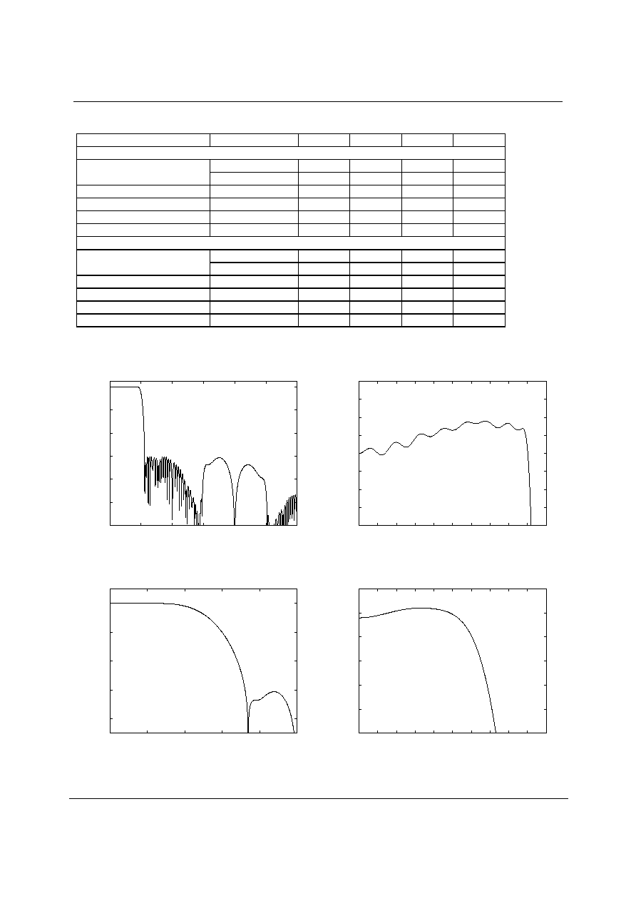
Product Preview
WM8778
w
PP Rev 1.7 June 2004
45
DIGITAL FILTER CHARACTERISTICS
PARAMETER
TEST CONDITIONS
MIN
TYP
MAX
UNIT
ADC Filter
±0.01 dB
0
0.4535fs
Passband
-6dB
0.5fs
Passband ripple
±0.01
dB
Stopband
0.5465fs
Stopband Attenuation
f > 0.5465fs
-65
dB
Group Delay
22
fs
DAC Filter
±0.05 dB
0.454fs
Passband
-3dB
0.4892
fs
Passband ripple
±0.05
dB
Stopband
0.546fs
Stopband Attenuation
f > 0.546fs
-60
dB
Group Delay
19
fs
Table 15 Digital Filter Characteristics
DAC FILTER RESPONSES
-120
-100
-80
-60
-40
-20
0
0
0.5
1
1.5
2
2.5
3
Response (dB)
Frequency (Fs)
Figure 25 DAC Digital Filter Frequency Response ≠ 44.1, 48
and 96kHz
-0.2
-0.15
-0.1
-0.05
0
0.05
0.1
0.15
0.2
0
0.05
0.1
0.15
0.2
0.25
0.3
0.35
0.4
0.45
0.5
Response (dB)
Frequency (Fs)
Figure 26 DAC Digital Filter Ripple ≠ 44.1, 48 and 96kHz
-80
-60
-40
-20
0
0
0.2
0.4
0.6
0.8
1
Response (dB)
Frequency (Fs)
Figure 27 DAC Digital Filter Frequency Response ≠ 192kHz
-1
-0.8
-0.6
-0.4
-0.2
0
0.2
0
0.05
0.1
0.15
0.2
0.25
0.3
0.35
0.4
0.45
0.5
Response (dB)
Frequency (Fs)
Figure 28 DAC Digital filter Ripple - 192kHz
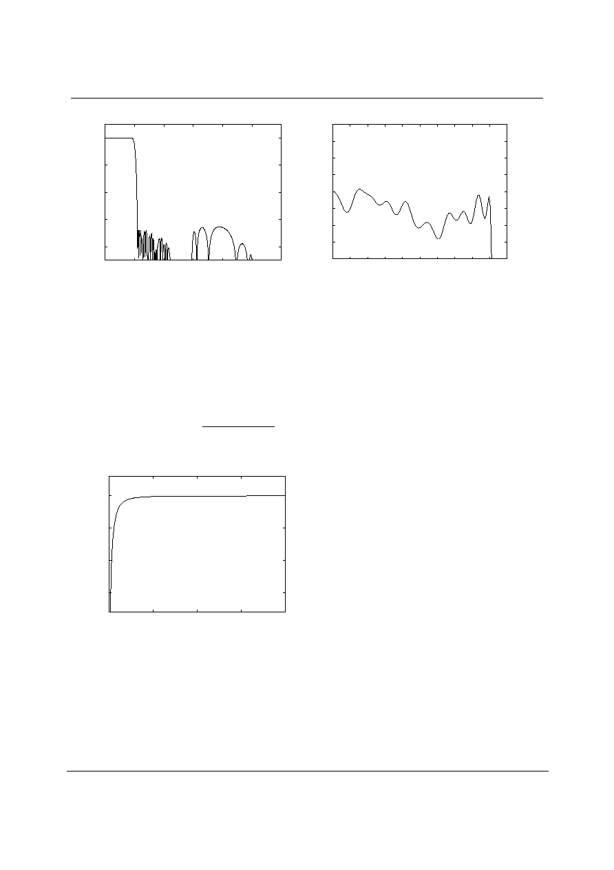
WM8778
Product Preview
w
PP Rev 1.7 June 2004
46
ADC FILTER RESPONSES
-80
-60
-40
-20
0
0
0.5
1
1.5
2
2.5
3
Response (dB)
Frequency (Fs)
Figure 29 ADC Digital Filter Frequency Response
-0.02
-0.015
-0.01
-0.005
0
0.005
0.01
0.015
0.02
0
0.05
0.1
0.15
0.2
0.25
0.3
0.35
0.4
0.45
0.5
Response (dB)
Frequency (Fs)
Figure 30 ADC Digital Filter Ripple
ADC HIGH PASS FILTER
The WM8778 has a selectable digital highpass filter to remove DC offsets. The filter response is characterised by the
following polynomial.
Figure 31 ADC Highpass Filter Response
1 - z
-1
1 - 0.9995z
-1
H(z) =
-15
-10
-5
0
0
0.0005
0.001
0.0015
0.002
Response (dB)
Frequency (Fs)
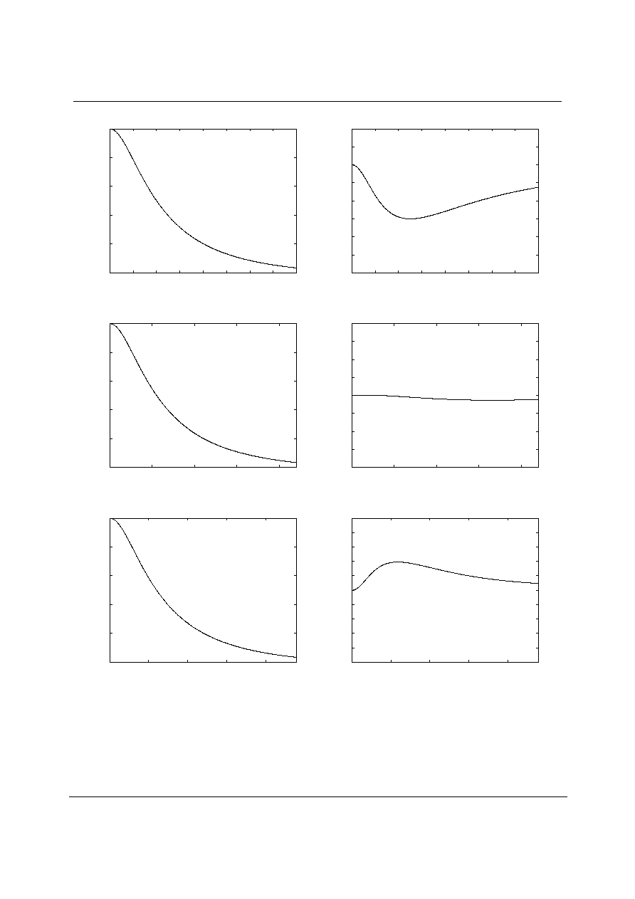
Product Preview
WM8778
w
PP Rev 1.7 June 2004
47
DIGITAL DE-EMPHASIS CHARACTERISTICS
-10
-8
-6
-4
-2
0
0
2
4
6
8
10
12
14
16
Response (dB)
Frequency (kHz)
Figure 32 De-Emphasis Frequency Response (32kHz)
-3
-2.5
-2
-1.5
-1
-0.5
0
0.5
1
0
2
4
6
8
10
12
14
16
Response (dB)
Frequency (kHz)
Figure 33 De-Emphasis Error (32KHz)
-10
-8
-6
-4
-2
0
0
5
10
15
20
Response (dB)
Frequency (kHz)
Figure 34 De-Emphasis Frequency Response (44.1KHz)
-0.4
-0.3
-0.2
-0.1
0
0.1
0.2
0.3
0.4
0
5
10
15
20
Response (dB)
Frequency (kHz)
Figure 35 De-Emphasis Error (44.1KHz)
-10
-8
-6
-4
-2
0
0
5
10
15
20
Response (dB)
Frequency (kHz)
Figure 36 De-Emphasis Frequency Response (48kHz)
-1
-0.8
-0.6
-0.4
-0.2
0
0.2
0.4
0.6
0.8
1
0
5
10
15
20
Response (dB)
Frequency (kHz)
Figure 37 De-Emphasis Error (48kHz)
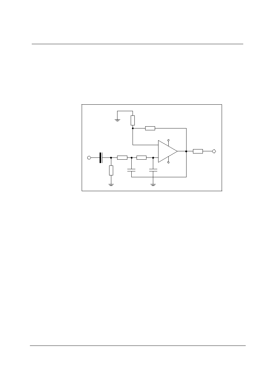
WM8778
Product Preview
w
PP Rev 1.7 June 2004
48
APPLICATIONS INFORMATION
RECOMMENDED EXTERNAL COMPONENTS
It is recommended that a low pass filter be applied to the output from the DAC for hi-fi applications.
Typically a second order filter is suitable and provides sufficient attenuation of high frequency
components (the unique low order, high bit count multi-bit sigma delta DAC structure used in
WM8778 produces much less high frequency output noise). This filter is typically also used to
provide the 2x gain needed to provide the standard 2Vrms output level from most consumer
equipment. Figure 34 shows a suitable post DAC filter circuit, with 2x gain. Alternative inverting filter
architectures might also be used with as good results.
+
_
+
+VS
-VS
10uF
51
7.5K
680pF
1.8k
10k
4.7k
4.7k
1.0nF
Figure 38 Recommended Post DAC Filter Circuit
Product Preview
WM8778
w
PP Rev 1.7 June 2004
49
PACKAGE DIMENSIONS
NOTES:
A. ALL LINEAR DIMENSIONS ARE IN MILLIMETERS.
B. THIS DRAWING IS SUBJECT TO CHANGE WITHOUT NOTICE.
C. BODY DIMENSIONS DO NOT INCLUDE MOLD FLASH OR PROTRUSION, NOT TO EXCEED 0.20MM.
D. MEETS JEDEC.95 MO-150, VARIATION = AH. REFER TO THIS SPECIFICATION FOR FURTHER DETAILS.
DM007.D
DS: 28 PIN SSOP (10.2 x 5.3 x 1.75 mm)
Symbols
Dimensions
(mm)
MIN
NOM
MAX
A
-----
-----
2.0
A
1
0.05
-----
0.25
A
2
1.65
1.75
1.85
b
0.22
0.30
0.38
c
0.09
-----
0.25
D
9.90
10.20
10.50
e
E
7.40
7.80
8.20
5.00
5.30
5.60
L
0.55
0.75
0.95
A A2
A1
14
1
15
28
E1
E
c
L
GAUGE
PLANE
0.25
e
b
D
SEATING PLANE
-C-
0.10 C
REF:
JEDEC.95, MO-150
E
1
L
1
0.125 REF
0.65 BSC
L
1
0
o
4
o
8
o

WM8778
Product Preview
w
PP Rev 1.7 June 2004
50
IMPORTANT NOTICE
Wolfson Microelectronics plc (WM) reserve the right to make changes to their products or to discontinue any product or
service without notice, and advise customers to obtain the latest version of relevant information to verify, before placing
orders, that information being relied on is current. All products are sold subject to the WM terms and conditions of sale
supplied at the time of order acknowledgement, including those pertaining to warranty, patent infringement, and limitation
of liability.
WM warrants performance of its products to the specifications applicable at the time of sale in accordance with WM's
standard warranty. Testing and other quality control techniques are utilised to the extent WM deems necessary to support
this warranty. Specific testing of all parameters of each device is not necessarily performed, except those mandated by
government requirements.
In order to minimise risks associated with customer applications, adequate design and operating safeguards must be used
by the customer to minimise inherent or procedural hazards. Wolfson products are not authorised for use as critical
components in life support devices or systems without the express written approval of an officer of the company. Life
support devices or systems are devices or systems that are intended for surgical implant into the body, or support or
sustain life, and whose failure to perform when properly used in accordance with instructions for use provided, can be
reasonably expected to result in a significant injury to the user. A critical component is any component of a life support
device or system whose failure to perform can be reasonably expected to cause the failure of the life support device or
system, or to affect its safety or effectiveness.
WM assumes no liability for applications assistance or customer product design. WM does not warrant or represent that
any license, either express or implied, is granted under any patent right, copyright, mask work right, or other intellectual
property right of WM covering or relating to any combination, machine, or process in which such products or services might
be or are used. WM's publication of information regarding any third party's products or services does not constitute WM's
approval, license, warranty or endorsement thereof.
Reproduction of information from the WM web site or datasheets is permissible only if reproduction is without alteration and
is accompanied by all associated warranties, conditions, limitations and notices. Representation or reproduction of this
information with alteration voids all warranties provided for an associated WM product or service, is an unfair and deceptive
business practice, and WM is not responsible nor liable for any such use.
Resale of WM's products or services with statements different from or beyond the parameters stated by WM for that
product or service voids all express and any implied warranties for the associated WM product or service, is an unfair and
deceptive business practice, and WM is not responsible nor liable for any such use.
ADDRESS:
Wolfson Microelectronics plc
Westfield House
26 Westfield Road
Edinburgh
EH11 2QB
United Kingdom
Tel :: +44 (0)131 272 7000
Fax :: +44 (0)131 272 7001
Email :: sales@wolfsonmicro.com