 | ÐлекÑÑоннÑй компоненÑ: WM8785 | СкаÑаÑÑ:  PDF PDF  ZIP ZIP |
Äîêóìåíòàöèÿ è îïèñàíèÿ www.docs.chipfind.ru
w
WM8785
24-Bit, 192kHz Stereo ADC
WOLFSON MICROELECTRONICS plc
To receive regular email updates, sign up
at
http://www.wolfsonmicro.com/enews/
Pre-Production, December 2005, Rev 3.0
Copyright
2005 Wolfson Microelectronics plc
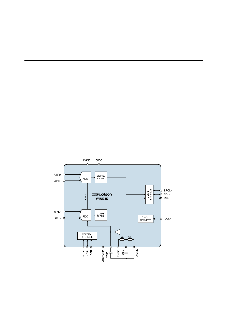
DESCRIPTION
The WM8785 is a stereo audio ADC with differential inputs
designed for high performance recordable media applications.
Data is provided as a PCM output.
Stereo 24-bit multi-bit sigma-delta ADCs are used with digital
audio output word lengths of 16 to 32 bits, and sampling rates
from 8kHz to 192kHz. The device has a selectable high pass
filter to remove residual DC offsets. The device also supports a
TDM bus for data out.
The device is controlled via a 2 or 3 wire serial interface. The
interface provides access to all features including oversampling
rate, audio format, powerdown, master/slave control and digital
signal manipulation. The device is supplied in a 20-lead SSOP
package.
FEATURES
· SNR 111dB (`A' weighted @ 48kHz)
· THD -102dB (at -0.1dB)
· Sampling Frequency: 8 192kHz
· 2 or 3 Wire Microprocessor Control Interface
· Master or Slave Clocking Mode
· Programmable Audio Data Interface Modes
-
I
2
S, Left, Right Justified or DSP
-
16/20/24/32 bit Word Lengths
· A TDM bus is supported for data out
· Supply Voltages
-
Analogue 4.5 to 5.5V
-
Digital core: 2.7V to 3.6V
· 20-lead SSOP package
APPLICATIONS
· Recordable DVD Players
· Personal Video Recorders
· High End Sound Cards
· Studio Audio Processing Equipment
BLOCK DIAGRAM

WM8785
Pre-Production
w
PP Rev 3.0 December 2005
2
TABLE OF CONTENTS
DESCRIPTION .......................................................................................................1
FEATURES.............................................................................................................1
APPLICATIONS .....................................................................................................1
BLOCK DIAGRAM .................................................................................................1
TABLE OF CONTENTS .........................................................................................2
PIN CONFIGURATION...........................................................................................3
ORDERING INFORMATION ..................................................................................3
PIN DESCRIPTION ................................................................................................4
ABSOLUTE MAXIMUM RATINGS .........................................................................5
RECOMMENDED OPERATING CONDITIONS .....................................................5
ELECTRICAL CHARACTERISTICS ......................................................................6
TERMINOLOGY ............................................................................................................ 7
SIGNAL TIMING REQUIREMENTS .......................................................................8
SYSTEM CLOCK TIMING ............................................................................................. 8
AUDIO INTERFACE TIMING MASTER MODE, PCM DATA ...................................... 8
AUDIO INTERFACE TIMING SLAVE MODE, PCM DATA ......................................... 9
CONTROL INTERFACE TIMING 3-WIRE MODE ...................................................... 9
CONTROL INTERFACE TIMING 2-WIRE MODE .................................................... 10
POWER-ON RESET ................................................................................................... 11
DIGITAL FILTER CHARACTERISTICS ...............................................................12
TERMINOLOGY .......................................................................................................... 12
FILTER RESPONSES ..........................................................................................13
DEVICE DESCRIPTION .......................................................................................16
INTRODUCTION ......................................................................................................... 16
DIGITAL AUDIO INTERFACE ..................................................................................... 16
DIGITAL HIGH PASS .................................................................................................. 20
DATA OUT PIN DISABLE ........................................................................................... 21
CONTROL INTERFACE.............................................................................................. 21
TIME DIVISION MULTIPLEXED DATA OUT............................................................... 22
TDM SELECTION ....................................................................................................... 23
OVERSAMPLING RATIOS AND SIGMA-DELTA MODULATOR FREQUENCY.......... 26
MASTER CLOCK AND AUDIO SAMPLE RATES........................................................ 26
MLCK AND LRCLK PHASE RELATIONSHIP.............................................................. 27
POWER DOWN CONTROL ........................................................................................ 27
REGISTER MAP ......................................................................................................... 28
APPLICATIONS INFORMATION .........................................................................29
RECOMMENDED EXTERNAL COMPONENTS .......................................................... 29
PACKAGE DIMENSIONS ....................................................................................30
IMPORTANT NOTICE..........................................................................................31
ADDRESS: .................................................................................................................. 31
Pre-Production
WM8785
w
PP Rev 3.0 December 2005
3
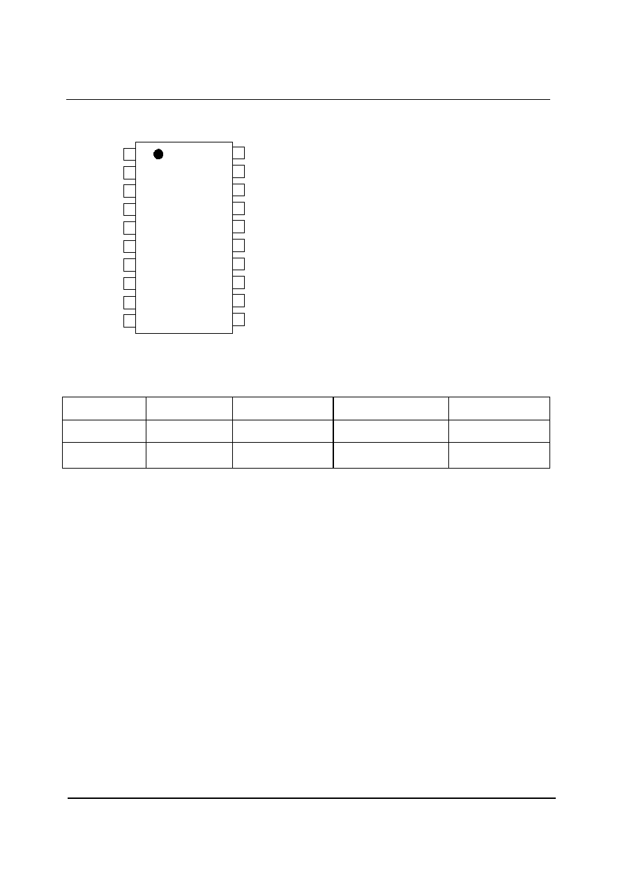
PIN CONFIGURATION
1
2
3
4
5
6
7
8
VMID
CSB
NC
DVDD
DGND
AINR-
AINR+
AINL-
VREF
LRCLK
NC
AGND
AVDD
AINL+
VREFGND
DOUT
13
14
15
16
17
20
19
18
9
10
BCLK
MCLK
SCLK
SDIN
11
12
ORDERING INFORMATION
ORDER CODE
TEMPERATURE
RANGE
PACKAGE
MOISTURE SENSITIVITY
LEVEL
PEAK SOLDERING
TEMPERATURE
WM8785GEDS/V
-25
°C to +85°C
20-lead SSOP
(Pb-free)
MSL3
260
o
C
WM8785GEDS/RV
-25
°C to +85°C
20-lead SSOP
(Pb-free, tape and reel)
MSL3
260
o
C
Note:
Reel quantity = 2,000
WM8785
Pre-Production
w
PP Rev 3.0 December 2005
4
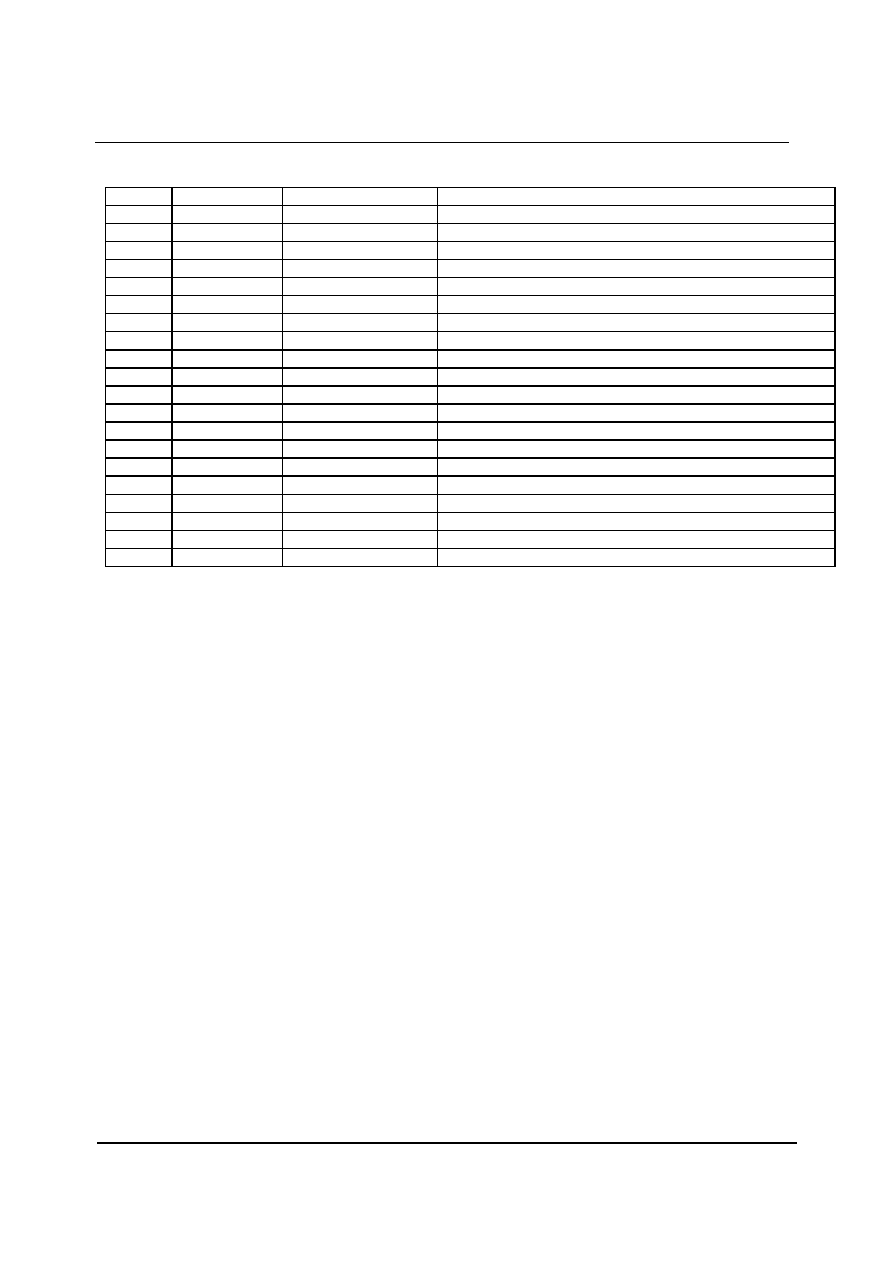
PIN DESCRIPTION
PIN
NAME
TYPE
DESCRIPTION
1
AINL+
Analogue Input
Left Channel Positive Input
2
AINL-
Analogue Input
Left Channel Negative Input
3
VREFGND
Analogue Reference
Negative Reference Connection
4
AVDD
Supply
Analogue Supply
5
AGND
Supply
Analogue Ground (return path for AVDD)
6
LRCLK
Digital Input / Output
Audio Interface Left / Right Clock
7
DOUT
Digital Output
ADC Digital Audio Data
8
BCLK
Digital Input / Output
Audio Interface Bit Clock
9
MCLK
Digital Input
Master Clock
10
NC
NC
No Connection
11
SCLK
Digital Input
Control Interface Clock Input / 2 wire output
12
SDIN
Digital Input / Output
Control Interface Data Input
13
CSB
Digital Input
Chip Select / Control Interface Format Selection / 3 wire address select
14
NC
NC
No connection
15
DVDD
Supply
Digital Supply
16
DGND
Supply
Digital Ground (return path for DVDD)
17
VMID
Analogue Output
Midrail Voltage Decoupling Capacitor
18
VREF
Analogue Reference
Reference Voltage Decoupling Capacitor
19
AINR-
Analogue Input
Right Channel Negative Input
20
AINR+
Analogue Input
Right Channel Positive Input
Pre-Production
WM8785
w
PP Rev 3.0 December 2005
5
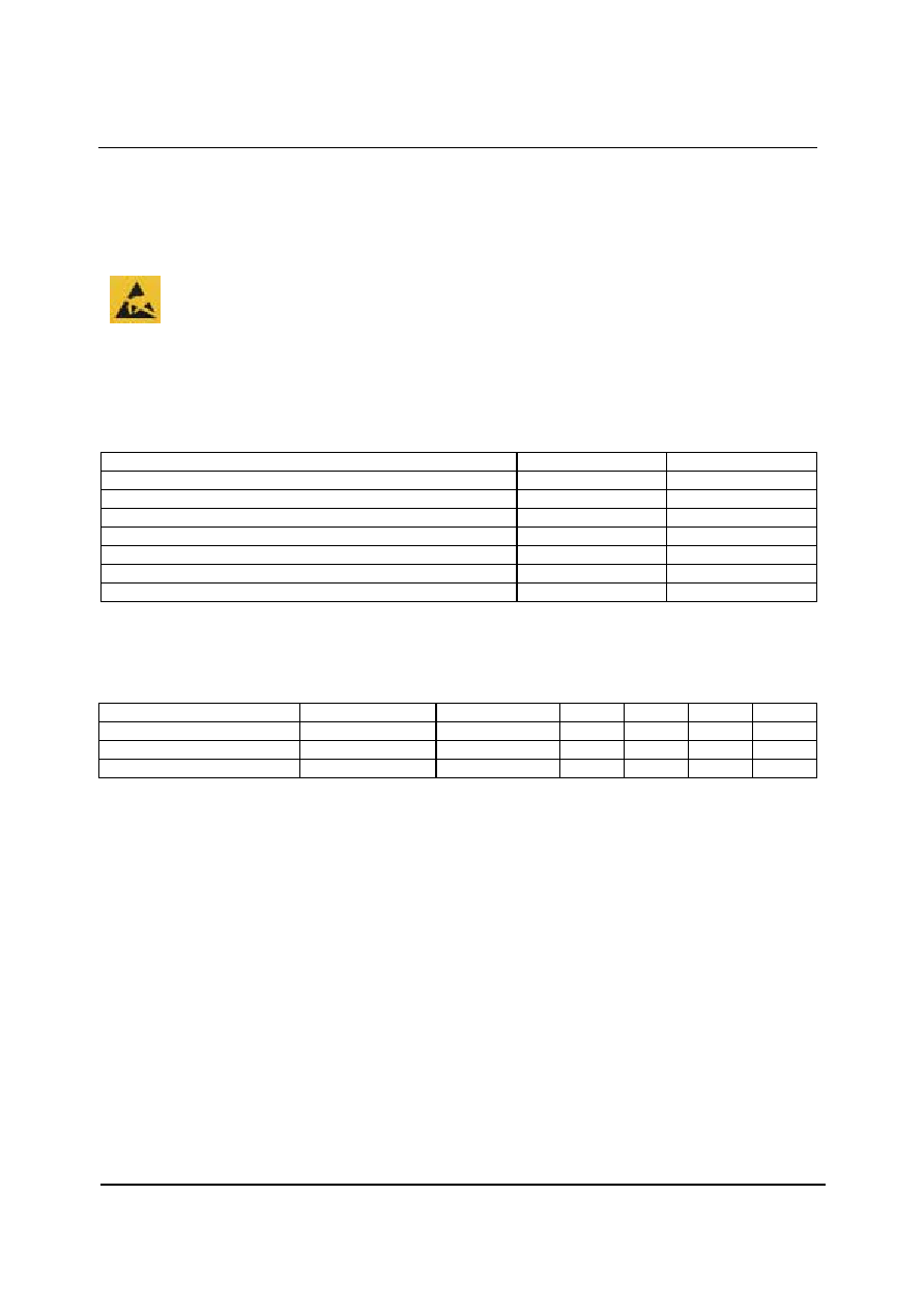
ABSOLUTE MAXIMUM RATINGS
Absolute Maximum Ratings are stress ratings only. Permanent damage to the device may be caused by continuously
operating at or beyond these limits. Device functional operating limits and guaranteed performance specifications are given
under Electrical Characteristics at the test conditions specified.
ESD Sensitive Device. This device is manufactured on a CMOS process. It is therefore generically susceptible
to damage from excessive static voltages. Proper ESD precautions must be taken during handling and storage
of this device.
Wolfson tests its package types according to IPC/JEDEC J-STD-020B for Moisture Sensitivity to determine acceptable storage
conditions prior to surface mount assembly. These levels are:
MSL1 = unlimited floor life at <30
°C / 85% Relative Humidity. Not normally stored in moisture barrier bag.
MSL2 = out of bag storage for 1 year at <30
°C / 60% Relative Humidity. Supplied in moisture barrier bag.
MSL3 = out of bag storage for 168 hours at <30
°C / 60% Relative Humidity. Supplied in moisture barrier bag.
The Moisture Sensitivity Level for each package type is specified in Ordering Information.
CONDITION
MIN
MAX
Digital supply voltage
-0.3V
+3.63V
Analogue supply voltage
-0.3V
+7V
Voltage range digital inputs
DGND -0.3V
DVDD + 0.3V
Voltage range analogue inputs
AGND -0.3V
AVDD +0.3V
Master Clock Frequency
40MHz
Operating temperature range, T
A
-25
°C
+85
°C
Storage temperature after soldering
-65
°C
+150
°C
Note: Analogue and digital grounds must always be within 0.3V of each other.
RECOMMENDED OPERATING CONDITIONS
PARAMETER
SYMBOL
TEST CONDITIONS
MIN
TYP
MAX
UNIT
Digital supply range
DVDD
2.7
3.6
V
Analogue supply range
AVDD
4.5
5.5
V
Ground
DGND,AGND
0
V
Document Outline
- WM8785
- 24-Bit, 192kHz Stereo ADC
- DESCRIPTION
- FEATURES
- APPLICATIONS
- BLOCK DIAGRAM
- TABLE OF CONTENTS
- PIN CONFIGURATION
- ORDERING INFORMATION
- PIN DESCRIPTION
- ABSOLUTE MAXIMUM RATINGS
- RECOMMENDED OPERATING CONDITIONS
- ELECTRICAL CHARACTERISTICS
- SIGNAL TIMING REQUIREMENTS
- SYSTEM CLOCK TIMING
- AUDIO INTERFACE TIMING
MASTER MODE, PCM DATA
- AUDIO INTERFACE TIMING
SLAVE MODE, PCM DATA
- CONTROL INTERFACE TIMING
3-WIRE MODE
- CONTROL INTERFACE TIMING
2-WIRE MODE
- POWER-ON RESET
- DIGITAL FILTER CHARACTERISTICS
- TERMINOLOGY
- FILTER RESPONSES
- SINGLE RATE 48k
- DUAL RATE 96k
- QUAD RATE 192k
- DEVICE DESCRIPTION
- INTRODUCTION
- DIGITAL AUDIO INTERFACE
- DIGITAL HIGH PASS
- DATA OUT PIN DISABLE
- CONTROL INTERFACE
- TIME DIVISION MULTIPLEXED DATA OUT
- TDM SELECTION
- OVERSAMPLING RATIOS AND SIGMA-DELTA MODULATOR FREQUENCY
- MASTER CLOCK AND AUDIO SAMPLE RATES
- MLCK AND LRCLK PHASE RELATIONSHIP
- POWER DOWN CONTROL
- REGISTER MAP
- APPLICATIONS INFORMATION
- RECOMMENDED EXTERNAL COMPONENTS
- PACKAGE DIMENSIONS
- IMPORTANT NOTICE
- ADDRESS: