Document Outline
- WM8802
- Digital Audio Interface Transceiver
- DESCRIPTION
- FEATURES
- APPLICATIONS
- BLOCK DIAGRAM
- PIN CONFIGURATION
- ORDERING INFORMATION
- PIN DESCRIPTION
- ABSOLUTE MAXIMUM RATINGS
- RECOMMENDED OPERATING CONDITIONS
- ELECTRICAL CHARACTERISTICS
- DC CHARACTERISTICS
- AC CHARACTERISTICS
- MICROCONTROLLER INTERFACE AC CHARACTERISTICS
- DEVICE DESCRIPTION
- INITIAL SYSTEM SETTINGS
- SYSTEM RESET (XMODE)
- CHIP ADDRESS SETTINGS (EMPHA/UO,AUDIO/VO)
- DEMODULATION FUNCTION MASTER/SLAVE SETTINGS (CKST )
- MODULATION FUNCTION AND GENERAL-PURPOSE I/O PORT SWITCHING (INT )
- DESCRIPTION OF DEMODULATION FUNCTION
- CLOCKS
- BI-PHASESIGNAL INPUT /OUTPUT
- SERIAL AUDIO DATA INPUT/OUTPUT
- ERROR OUTPUT PROCESSING
- CHANNEL STATUS OUTPUT
- OTHER OUTPUTS
- IEC61937,DTS-CD/LD DETECTION FLAG OUTPUT
- DESCRIPTION OF MODULATION FUNCTION AND GENERAL-PURPOSE I/OS
- MODULATION FUNCTION USAGEMETHOD
- GENERAL PURPOSE I/O (GPIO0,GPIO1,GPIO2,GPIO3,GPIOEN)
- MICRO-CONTROLLER INTERFACE (INT ,CL,CE,DI,DO)
- DESCRIPTION OF MICRO-CONTROLLER INTERFACE
- WRITE DATA
- READ DATA
- BURST PREAMBLE PC FIELD
- RECOMMENDED EXTERNAL COMPONENTS
- SAMPLE APPLICATION
- RECOMMENDED EXTERNAL COMPONENTS VALUES
- PACKAGE DRAWING
- IMPORTANT NOTICE
WM8802
Digital Audio Interface Transceiver
WOLFSON MICROELECTRONICS plc
w :: www.wolfsonmicro.com
Product Preview, May 2003, Rev 1.0
Copyright
2003 Wolfson Microelectronics plc
DESCRIPTION
The WM8802 is a digital audio interface transceiver
conforming to IEC 60958/61937 and EIAJ CP-1201. The
device supports data sampling input rates of up to 192 kHz.
Data input to the serial digital audio data input pin can also
be modulated. The WM8802 features up to 6 data inputs
and 1 data output.
Data can be demodulated using the on-board PLL or with
the use of an external clock source.
The WM8802 is controlled via a 4-wire CCB compatible
control interface.
This interface provides access to the
channel status bits. The WM8802 also provides a number
of flag outputs including PCM data valid, de-emphasis, lock
and IEC 61937, DTS-CD/LD detection.
The device is available in a small 48-pin SQFP package.
FEATURES
�
PLL circuit for synchronization with transferred input bi-
phase mark signal.
�
Input sampling frequency: 32kHz to 192kHz
�
Outputs clocks: fs, fs/2, 2fs, 32fs, 64fs, 128fs, 256fs,
384fs, and 512fs.
�
4-Wire CCB MPU Serial Control or Hardware Default
Interface
�
Master or Slave Clocking Mode
�
Programmable Audio Data Interface Modes
-
I
2
S, Left, Right Justified
-
16/20/24/32 bit Word Lengths
�
3.3V Digital supply Operation
�
5V tolerant digital input ports
APPLICATIONS
�
DVD Receivers
�
AV Amplifiers
�
DVD Recorders
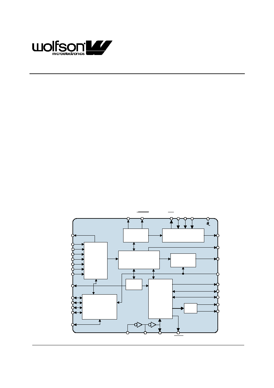
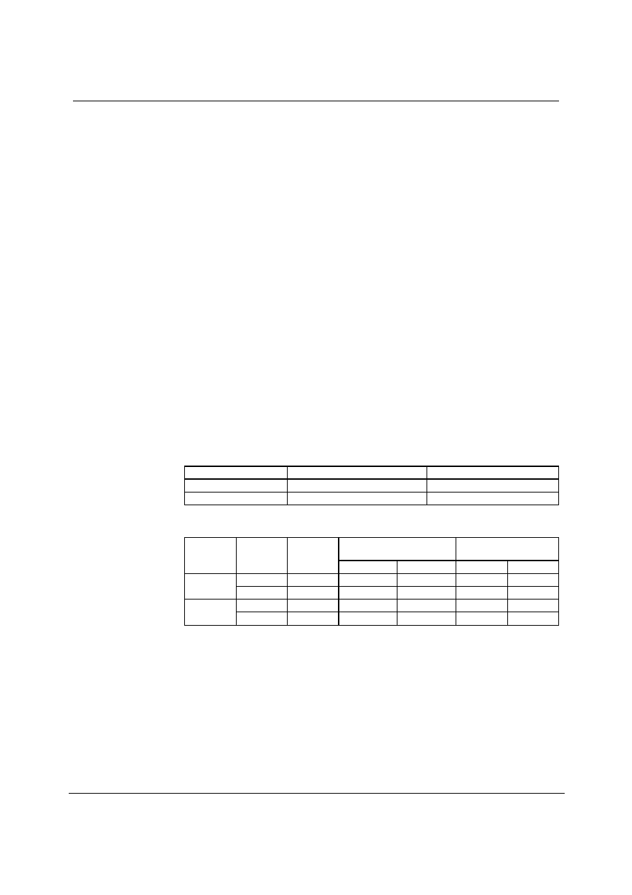
BLOCK DIAGRAM
DEMODULATION
AND
LOCK DETECT
INPUT
SELECTOR
MICROCONTROLLER
I/F
DATA
SELECTOR
CBIT, UBIT
1/N
MODULATION
AND
PARALLEL PORT
PLL
CLOCK
SELECTOR
W
WM8802
EMPH/UO
AUDIO/VO
INT CL CE DI
XMODE
DO
RERR
RDATA
SDIN
RMCK
RBCK
RLRCK
SBCK
SLRCK
RXOUT
RX0
RX1
RX2
RX3
RX4
RX5/VI
RX6/UI
TXO/GPIOEN
TDATA/GPIO3
TLRCLK/GPIO2
TBCLK/GPIO1
TMCLK/GPIO0
LPF
XMCLK
XOUT
XIN
CKST
WM8802
Product Preview
w
PP Rev 1.0 May 2003
2
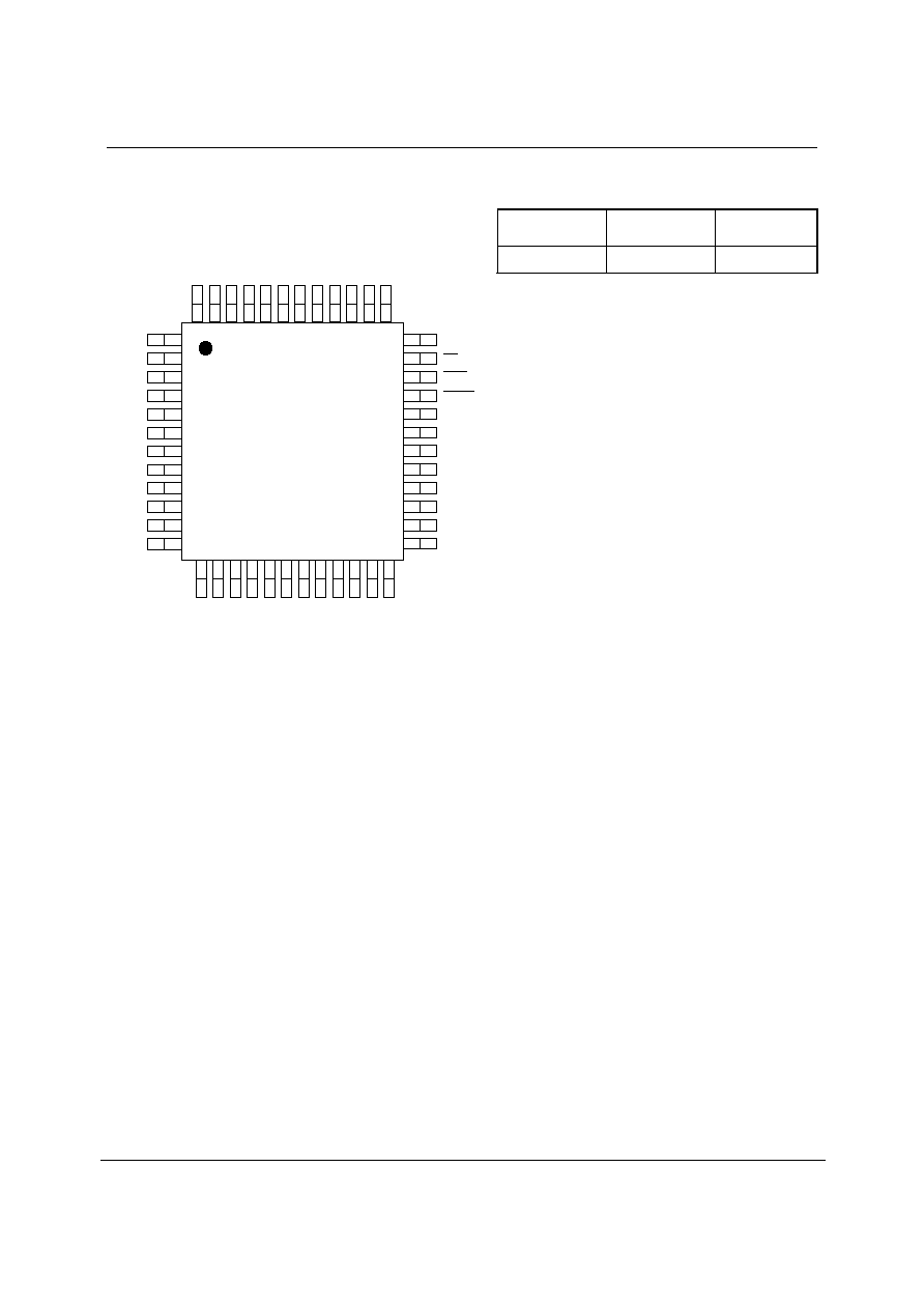
PIN CONFIGURATION
ORDERING INFORMATION
DEVICE
TEMP. RANGE
PACKAGE
WM8802CFR
0 to +70
o
C
48-pin SQFP
XMCK
DGND
DVDD
XOUT
R
L
RCK
DG
ND
DV
D
D
R
DAT
A
S
BCK
RXOUT
DVDD
DGND
RX3
RX2
RX1
RXO
RX4
RX5/VI
DVDD
TX
O
/
GP
I
O
EN
DV
D
D
T
M
CK/
G
P
I
O
0
T
M
CK/
G
P
I
O
1
T
L
RCK/
G
P
I
O
2
T
L
RCK/
G
P
I
O
3
XMO
D
E
DG
ND
AUDIO/VO
EMPH/UO
1
9
8
7
6
5
4
3
2
11
10
13 14 15 16 17 18 19
29
28
27
26
25
31
30
48 47 46 45 44 43 42
R
BCK
RX6/VI
S
L
RCK
DO
DI
RERR
CE
CL
41 40 39 38 37
XIN
CKST
DVDD
DGND
DGND
LP
F
AV
DD
RM
C
K
12
AG
ND
20 21 22 23 24
34
33
32
36
35
INT
SD
I
N
Product Preview
WM8802
w
PP Rev 1.0 May 2003
3
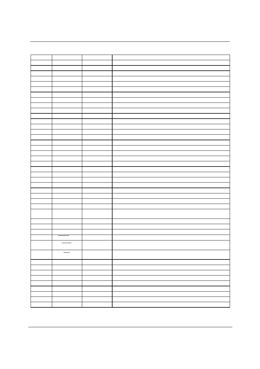
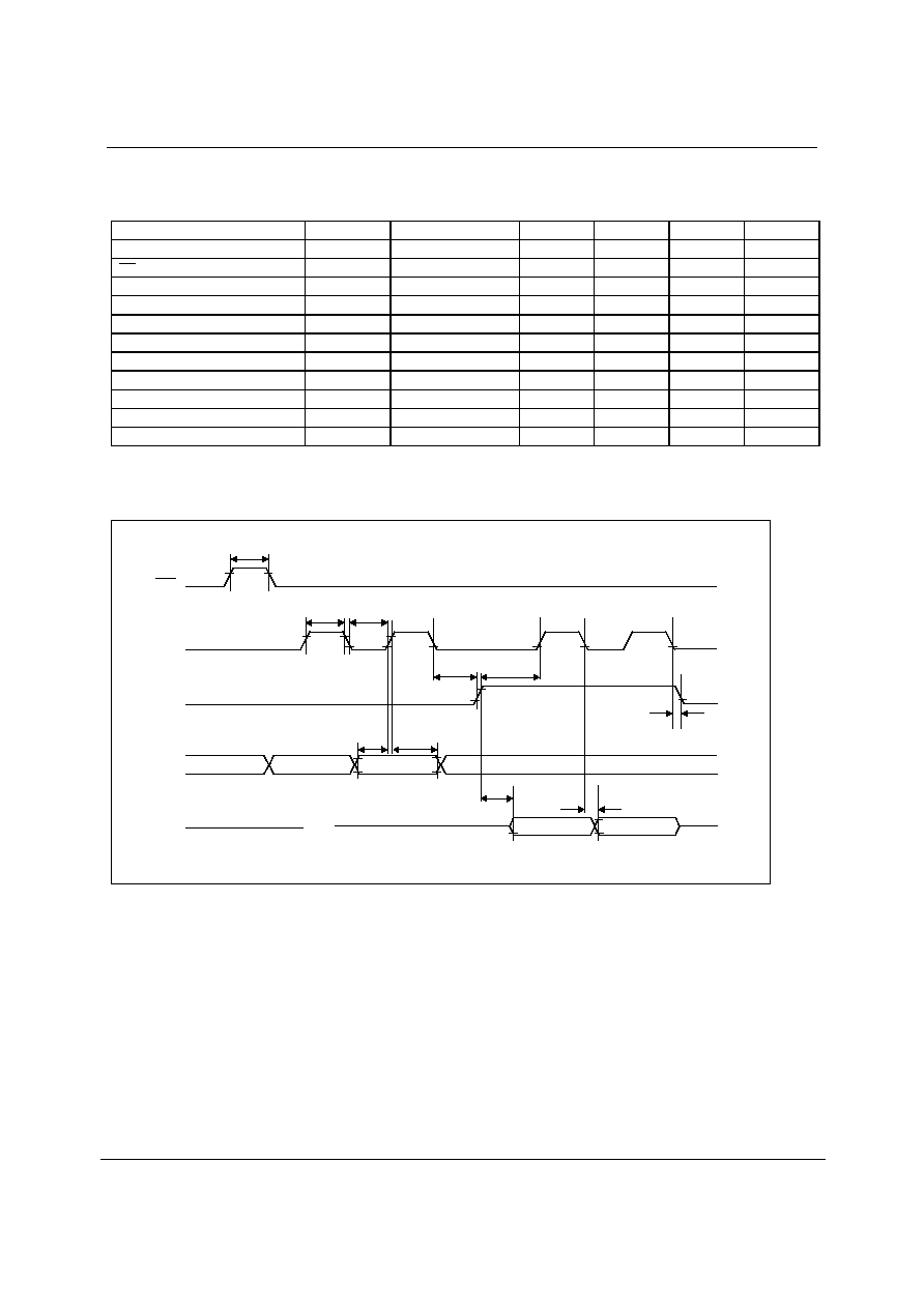
PIN DESCRIPTION
PIN
NAMETYPE
DE
SCRIPTION
1
RXOUT
Digital Output
Input bi-phase selection data output pin
2
RX0
Digital Input
1
TTL-compatible digital data input pin
3
RX1
Digital Input
Coaxial-compatible digital data input pin with built-in amplifier
4
RX2
Digital Input
1
TTL-compatible digital data input pin
5
RX3
Digital Input
1
TTL-compatible digital data input pin
6
DGND
Supply
Digital GND
7
DVDD
Supply
Digital power supply
8
RX4
Digital Input
1
TTL-compatible digital data input pin
9
RX5/VI
Digital Input
1
TTL-compatible digital data. Validity flag input pin for modulation.
10
RX6/UI
Digital Input
1
TTL-compatible digital data. User data input pin for modulation.
11
DVDD
Supply
PLL digital power supply
12
DGND
Supply
PLL digital GND
13
LPF
Analogue Output
PLL loop filter connection pin
14
AVDD
Supply
PLL analog power supply
15
AGND
Supply
PLL analog GND
16
RMCK
Digital Output
R system clock output pin (256fs, 512fs, XIN, VCO)
17
RBCK
Digital Output/Input R bit clock input/output pin (64fs)
18
DGND
Supply
Digital GND
19
DVDD
Supply
Digital power supply
20
RLRCK
Digital Output/Input R LR clock input/output pin (fs)
21
RDATA
Digital Output
Serial audio data input pin
22
SBCK
Digital Output
S bit clock output pin (32fs, 64fs, 128fs)
23
SLRCK
Digital Output
S LR clock output pin (fs/2, fs, 2fs)
24
SDIN
Digital Input
1
Serial audio data input pin
25
DGND
Supply
Digital GND
26
DVDD
Supply
Digital power supply
27
XMCK
Analogue Output
Oscillation amplifier output pin
28
XOUT
Analogue Output
Crystal resonator connection output pin
29
XIN
Analogue Input
Crystal resonator connection, external supply clock input pin (24.576 MHz or
12.288 MHz)
30
DVDD
Supply
Digital power supply
31
DGND
Supply
Digital GND
32
EMPH/UO
Digital Input/Output Emphasis information, U data output. Chip address setting pin
2
.
33
AUDIO/VO
Digital Input/Output Non-PCM output, V flag output. Chip address setting pin
2
.
34
CKST
Digital Input/Output
Clock switch transition period signal. Demodulation master or slave
function switch pin
3
.
35
INT
Digital Input/Output
Micro-controller interrupt output. Modulation or general-purpose I/O switch
pin
4
.
36
RERR
Digital Output
PLL clock error, data error flag output
37
DO
Digital Output
Micro-controller I/F read data output pin (3-state)
38
DI
Digital Input
1
Micro-controller I/F write data input pin
39
CE
Digital Input
1
Micro-controller I/F chip enable input pin
40
CL
Digital Input
Micro-controller I/F clock input pin
41
XMODE
Digital Input
1
System reset input pin
42
DGND
Supply
Digital GND
43
DVDD
Supply
Digital power supply
44
TMCK/GPIO0
Digital Input/Output Modulation 256fs system clock input. General-purpose I/O input/output pin.

WM8802
Product Preview
w
PP Rev 1.0 May 2003
4
PIN
NAMETYPE
DE
SCRIPTION
45
TBCK/GPIO1
Digital Input/Output Modulation 64fs bit clock input. General-purpose I/O input/output pin.
46
TLRCK/GPIO2
Digital Input/Output Modulation fs clock input. General-purpose I/O input/output pin.
47
TDATA/GPIO3
Digital Input/Output Modulation serial audio data input. General-purpose I/O input/output pin.
48
TXO/GPIOEN
Digital Output/Input Modulation data output. General-purpose I/O enable input pin.
Notes:
1.
Input/output I or O
= -
0.3 to 3.6V, except annotated pins:
-
0.3 to +5.5V
2.
Pins 32 and 33 are latch address setting input pins when pin 41
=
Low.
3.
Pin 34 is the demodulation function master or slave setting input pin when pin 41 = Low.
4.
Pin 35 is the modulation function or general-purpose I/O function switch setting input pin when pin 41 = Low.
5.
Perform ON/OFF for all power supplies with the same timing as a latch-up countermeasure.
Product Preview
WM8802
w
PP Rev 1.0 May 2003
5
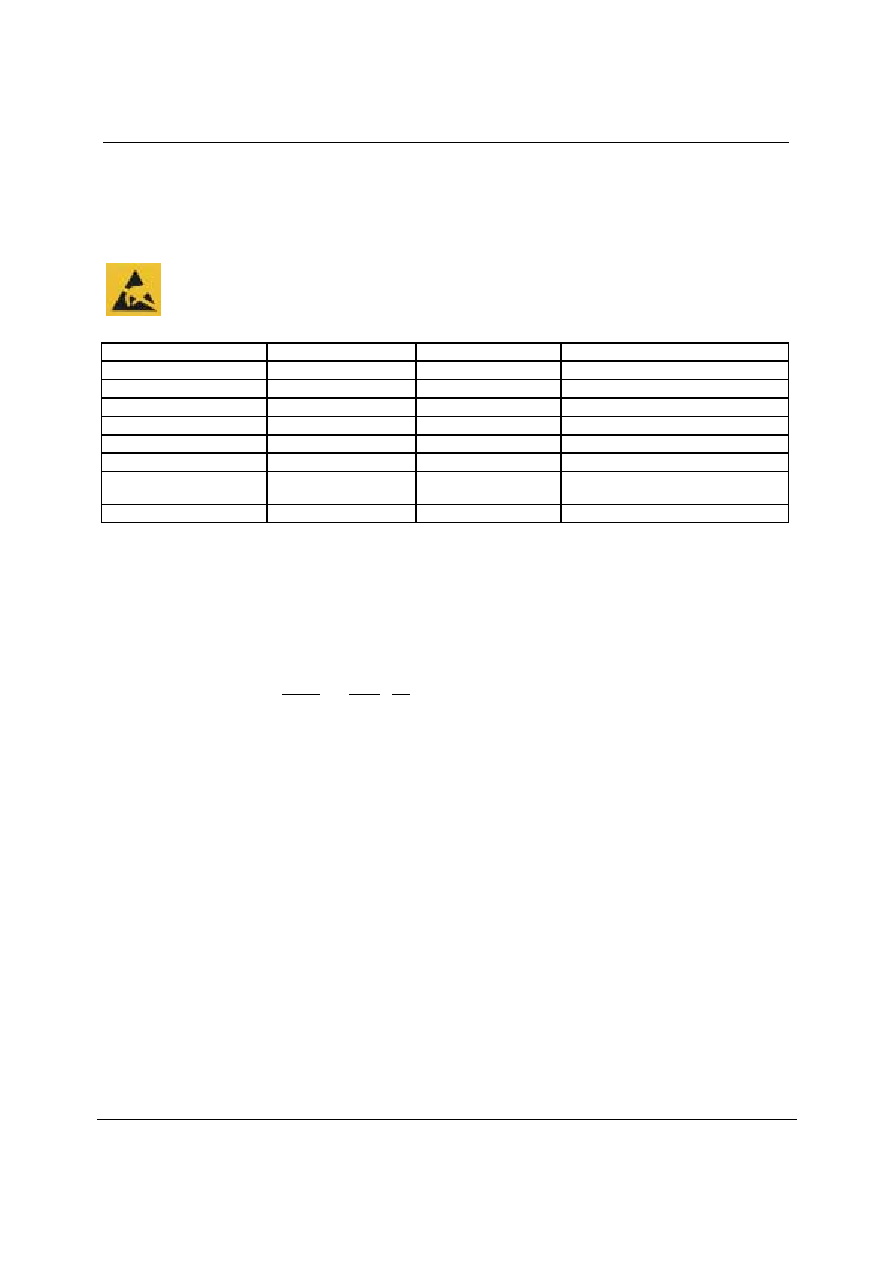
ABSOLUTEMAXIMUM RATINGS
Absolute Maximum Ratings are stress ratings only. Permanent damage to the device may be caused by continuously operating at
or beyond these limits. Device functional operating limits and guaranteed performance specifications are given under Electrical
Characteristics at the test conditions specified.
ESD Sensitive Device. This device is manufactured on a CMOS process. It is therefore generically susceptible
to damage from excessive static voltages. Proper ESD precautions must be taken during handling and storage
of this device.
CONDITION
SYMBOL
CONDITIONS
MIN-MAX
Maximum supply voltage
AVDD
max
1
-
0.3 to 4.6V
Maximum supply voltage
DVDD
max
2
-
0.3 to 4.6V
Input voltage 1
V
i1
3
-
0.3 to DVDD
+
0.3V
Input voltage 2
V
i2
4
-
0.3 to 5.8V
Output voltage
V
o
5
-
0.3 to DVDD
+
0.3V
Storage ambient temperature
T
stg
-
55 to 125
o
C
Operating ambient
temperature
T
opg
-
30 to 70
o
C
Maximum input/output current
T
i,
T
o
6
�
20mA
Notes:
1.
AVDD pin
2.
DVDD pin
3.
RX1, RBCK, RLRCK, XIN pins
TMCK/GPIO0, TBCK/GPIO1, TLRCK/GPIO2, TDATA/GPIO3, TXO/GPIOEN pins
4.
RX0, RX2, RX3, RX4, RX5/VI, RX6/UI pins
SDIN, DI, CE, CL, XMODE pins
5.
RXOUT, RMCK, RBCK, RLRCK, SBCK, SLRCK, RDATA pins
XMCK, XOUT, EMPHA/UO, AUDIO /VO, CKST , INT , RERR, DO pins
TMCK/GPIO0, TBCK/GPIO1, TLRCK/GPIO2, TDATA/GPIO3, TXO/GPIOEN pins
6.
Per input/output pin
WM8802
Product Preview
w
PP Rev 1.0 May 2003
6
RECOMMENDED OPERATING CONDITIONS
PARAMETER
SYMBOL
TEST CONDITIONS
MIN
TYP
MAX
UNIT
Supply voltage
AVDD, DVDD
3.0
3.3
3.6
V
Input voltage range 1
V
IN1
1
0
3.3
3.6
V
Input voltage range 2
V
IN2
2
0
3.3
5.5
V
Operating temperature
V
opq
-30
-
70
o
C
Notes:
1.
RX1, RBCK, RLRCK, XIN pins
TMCK/GPIO0, TBCK/GPIO1, TLRCK/GPIO2, TDATA/GPIO3, TXO/GPIOEN pins
2.
RX0, RX2, RX3, RX4, RX5/VI, RX6/UI pins
SDIN, DI, CE, CL, XMODE pins
ELECTRICAL CHARACTERISTICS
DC CHARACTERISTICS
Test Conditions
DC Characteristics at T
a
= 25
o
C, AVDD = DVDD = 3.3V, AGND = DGND = 0V
PARAMETER
SYMBOL
TEST CONDITIONS
MIN
TYP
MAX
UNIT
Input, High
V
IH
1
0.7VDD
-
-
V
Input, Low
V
IL
-
-
0.2VDD
V
Input, High
V
IH
2
2.0
-
5.8
V
Input, Low
V
IL
-
0.3
-
0.8
V
Output, High
V
OH
3
VDD
-
0.8
-
-
V
Output, Low
V
OL
-
-
0.4
V
Output, High
V
OH
4
VDD
-
0.8
-
-
V
Output, Low
V
OL
-
-
0.4
V
Output, High
V
OH
5
VDD
-
0.8
-
-
V
Output, Low
V
OL
-
-
0.4
V
Output, High
V
OH
6
VDD
-
0.8
-
-
V
Output, Low
V
OL
-
-
0.4
V
Input amplitude
V
PP
7
200
-
-
mV
Consumption current
V
DD1
8
-
1.7
3.4
mA
Consumption current
V
DD1
9
-
17
34
mA
Consumption current
V
DD1
10
-
19
38
mA
Notes:
1.
CMOS levels: RX1, RBCK, RLRCK, XIN pins
2.
TTL levels: Pins other than those listed above
3.
I
OH
=
-
12mA, I
OL
= 8mA: RMCK pin
4.
I
OH
=
-
8mA, I
OL
= 8mA: XMCK, XOUT pins
5.
I
OH
=
-
4mA, I
OL
= 4mA: RXOUT, RBCK, RLRCK, RDATA, SBCK pins
SLRCK, TMCK/GPIO0, TBCK/GPIO1, TLRCK/GPIO2 pins
TDATA/GPIO3, TXO/GPIOEN pins
6.
I
OH
=
-
2mA, I
OL
= 2mA: Pins other than those listed above
7.
Before capacitance of RX1 input pin
8.
Demodulation function and oscillation amplifier stopped, modulation only, output sampling frequency = 96kHz
9.
XIN continuous 24.576MHz oscillation, demodulation only, input sampling frequency = 96kHz
10.
XIN continuous 24.576MHz oscillation, modulation, input/output sampling frequency = 96kHz

Product Preview
WM8802
w
PP Rev 1.0 May 2003
7
AC CHARACTERISTICS
Test Conditions
AC Characteristics at T
a
= 25
o
C, AVDD = DVDD = 3.3V, AGND = DGND = 0V
PARAMETER
SYMBOL
TEST CONDITIONS
MIN
TYP
MAX
UNIT
RX0 TO RX6 sampling
frequency
f
RFS
28
-
195
kHz
XIN clock frequency
f
XF1
1
8
12.288
19
MHz
XIN clock frequency
f
XF2
2
20
24.576
30
MHz
RMCK clock frequency
f
RCK
4
-
100
MHz
RMCK clock jitter
t
j
-
200
-
ps
RMCK, RBCK delay
t
MBO
-
-
10
ns
RBCK, RDATA delay
t
BDO
-
-
10
ns
RMCK, SBC delay
t
MBO
3
-
-
10
ns
SMCK, RDATA delay
t
BDO
4
-
-
10
ns
TMCK input pulse width
t
WMI
10
-
-
ns
TBCK input pulse width
t
WBI
40
-
-
ns
TLRCK sampling frequency
f
TFS
28
-
195
kHz
TBCK, TDATA setup
t
DSI
-
20
-
ns
TBCK, TDATA hold
t
DHI
-
20
-
ns
TMCK, TBCK delay
t
MBI
-
-
10
ns
TBCK, TDATA delay
t
BDI
-
-
10
ns
Notes:
1.
XINSEL = "0" setting, 12.288MHz must be set when calculating input sampling frequency
2.
XINSEL = "1" setting, 24.576MHz must be set when calculating input sampling frequency
3.
When RMCK and SBCK source clocks are the same
4.
When SBCK is the PLL source clock
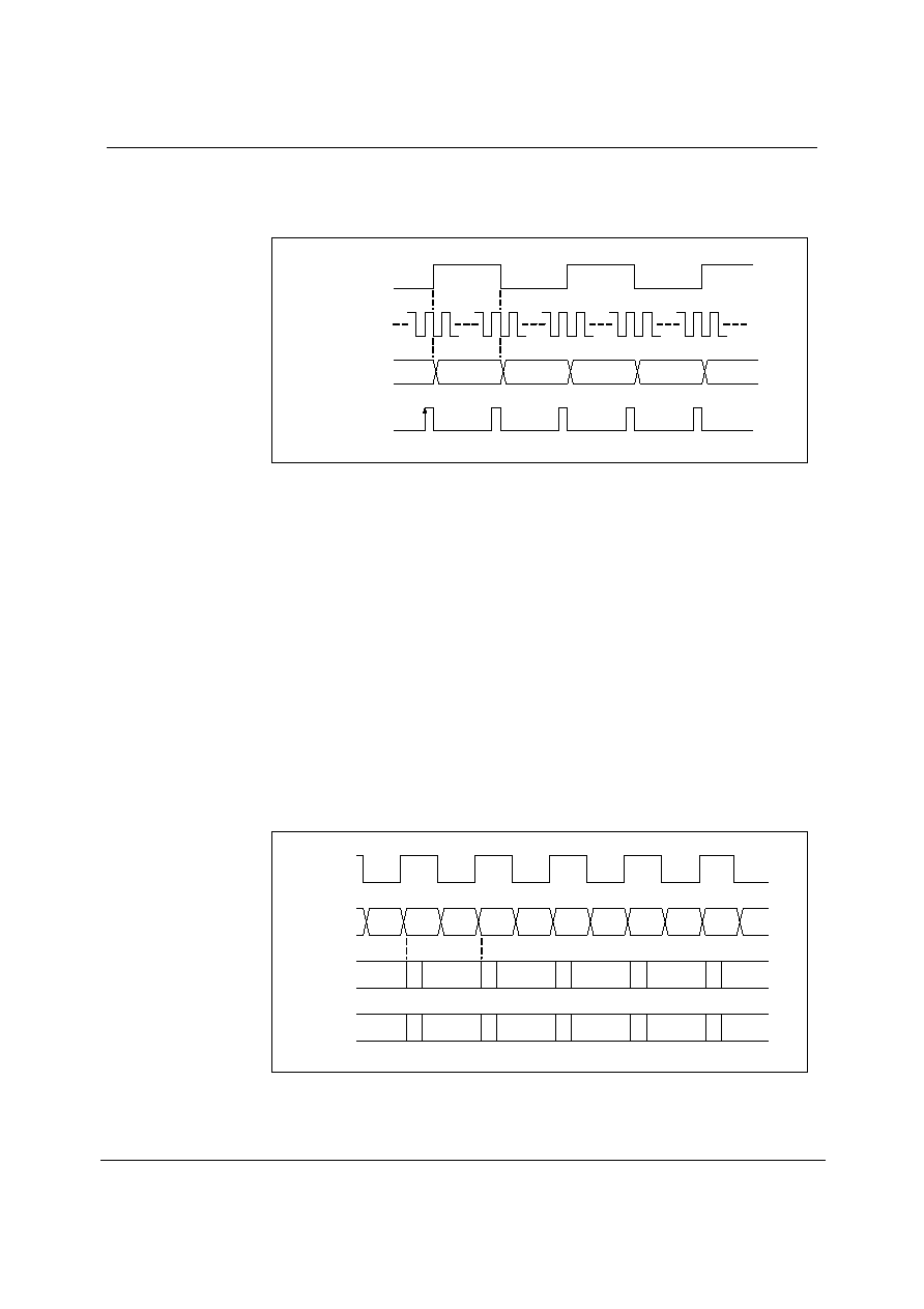
RBCK(O)
RDATA(O)
RLRCK(O)
t
WBI
t
BDO
t
WBI
TBCK(I)
TDATA(I)
TLRCK(I)
t
DSI
t
DHI
t
BDI
RMCK(O)
TMCK (I)
t
MBO
t
MBI
t
WMI
t
WMI
Figure 1 AC Characteristics
WM8802
Product Preview
w
PP Rev 1.0 May 2003
8
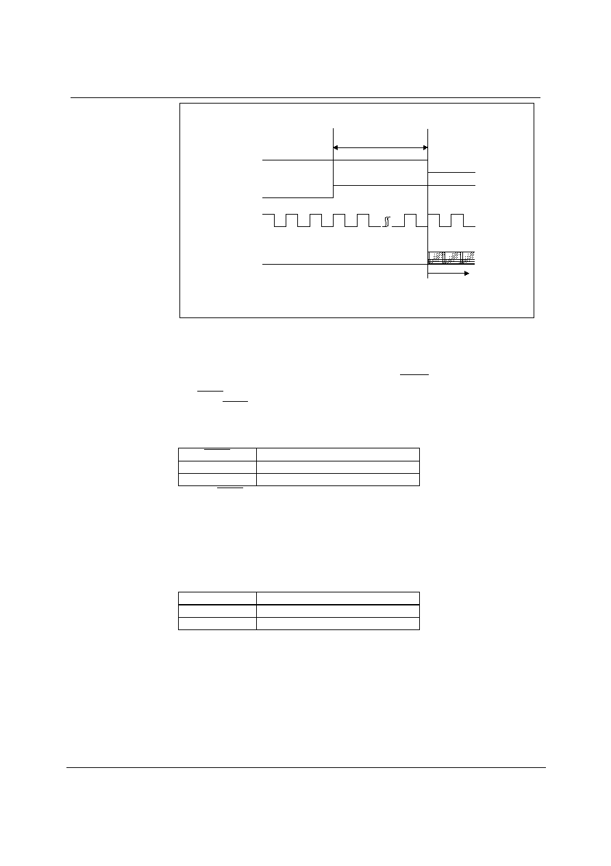
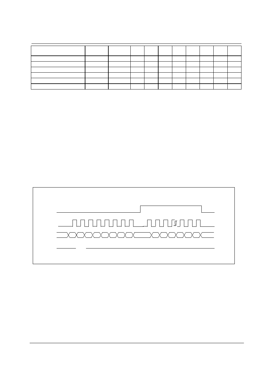
MICROCONTROLLER INTERFACE AC CHARACTERISTICS
Test Conditions
I/F AC Characteristics at T
a
= 25
o
C, AVDD = DVDD = 3.3V, AGND = DGND = 0V
PARAMETER
SYMBOL
TEST CONDITIONS
MIN
TYP
MAX
UNIT
XMODE pulse width, Low
t
RST dw
200
-
-
�
s
INT
pulse width, Low
t
INT uw
1
5
1/fs
36
�
s
CL pulse width, Low
t
CL dw
100
-
-
ns
CL pulse width, High
t
CL uw
100
-
-
ns
CL, CE setup time
t
CL setup
50
-
-
ns
CL, CE hold time
t
CE hold
50
-
-
ns
CL, DI setup time
t
DI setup
50
-
-
ns
CL, DE hold time
t
DI hold
50
-
-
ns
CL, CE hold time
t
CL hold
50
-
-
ns
CL, DO delay time
t
CL to DO
-
-
20
ns
CE, DO delay time
t
CE to DO
-
-
20
ns
Notes:
1.
When INTOPF is set to "1", fs = input sampling frequency
t
CLuw
t
INTuw
CL
CE
DI
t
CEtoDO
t
CLtoDO
INT
DO
t
CLdw
t
DIsetup
t
DIhold
t
CEsetup
t
CEhold
t
CLhold
Hi-Z
Figure 2 Micro-controller Interface AC Characteristics

Product Preview
WM8802
w
PP Rev 1.0 May 2003
9
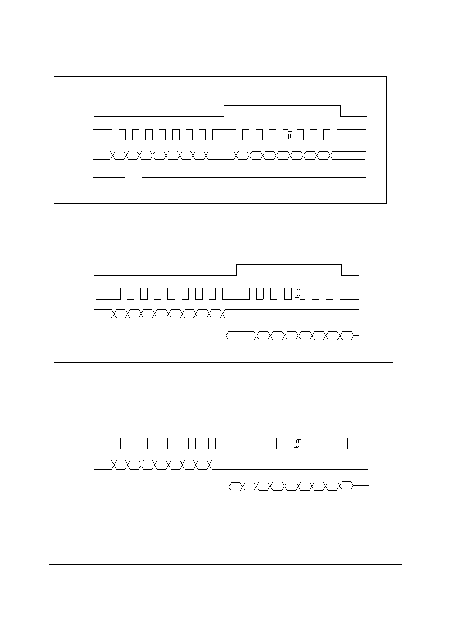
DEVICE DESCRIPTION
INITIAL SYSTEM SETTINGS
SYSTEM RESET (XMODE)
The system operates normally when XMODE is set to High after applying a supply voltage of 3.0V or
greater. Following power ON, the system is reset by setting XMODE to Low again.
A 10k
pull-down or pull-up resistor can be used to set EMPHA/UO, AUDIO /VO, CKST and
INT for the following:
�
chip address
�
demodulation function master or slave
�
modulation function or general-purpose I/O function settings
If EMPHA/UO, AUDIO /VO, CKST , and INT are not pulled up or down, their state is undefined. A
pull-up or pull-down resistor should always be connected to these pins.
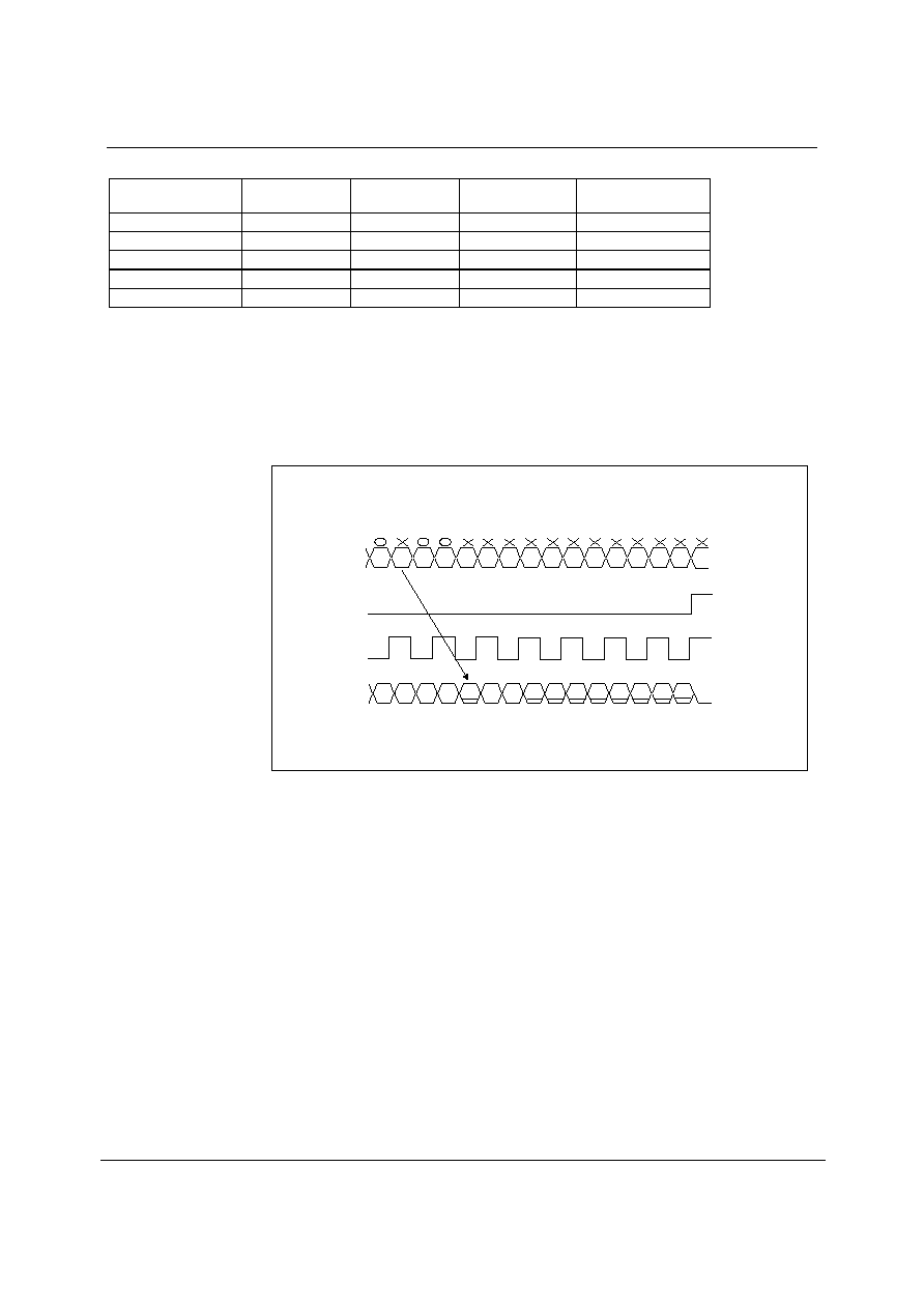
SETTING
PINS
Chip address
EMPHA/UO, AUDIO /VO
Demodulation function master or slave
CKST
Modulation function or general-
purpose I/O function
INT
Table 1 Pin Names and Settings
Set pin state
XMODE
DVDD
Normal system operation range
Setting completed
Undefined
Setting input
state
Output state
Setting input
state
Output state
Min 200
�
�
�
�
s
3.0V
3.3V
Figure 3 Setting Timing Chart of Function Setting Input Pins

WM8802
Product Preview
w
PP Rev 1.0 May 2003
10
CHIP ADDRESS SETTINGS (EMPHA/UO, AUDIO /VO)
The WM8802 comes with a function to set a unique chip address to allow the use of several
WM8802 on the same micro-controller bus.
A 10k
pull-down or pull-up resistor is used to set EMPHA/UO and AUDIO /VO as the chip address
settings. This allows up to set 4 chip addresses.
Chip addresses in the micro-controller interface can be set with CAL and CAU provided that they are
first two bits on the LSB side. CAL and CAU corresponds to the lower and higher chip address
respectively.
Address writing to a particular device is enabled by making the chip address setting, using
EMPHA/UO and AUDIO /VO, the same as the chip addresses sent from the micro-controller.
The chip address setting must be performed even when using only one WM8802 in the system. The
chip address is undefined and control from the micro-controller cannot be performed if the chip
address setting is not performed. While XMODE is Low and the micro-controller is not used the state
of the chip address setting pin is undefined,. Be sure to connect either A pull-down resistor or a pull-
up resistor should be connected to EMPHA/UO and AUDIO /VO.
AUDIO
/VO
EMPHA/UO
CAU
CAL
Pull-down
Pull-down
0
0
Pull-down
Pull-up
0
1
Pull-up
Pull-down
1
0
Pull-up
Pull-up
1
1
Table 2 Chipset Address Settings
INT
CKST
AUDIO/VO
EMPH/UO
WM8802
Pull-up 10k
External
Circuit
Pull-down 10k
Figure 4 Function Setting Input Pin Setting Example
Notes:
1.
Chip address setting
=> CAL = CAU = 0
2.
Demodulation function master or slave setting
=> Master
3.
Modulation function or general purpose I/O port switch => General purpose I/O port
function
Product Preview
WM8802
w
PP Rev 1.0 May 2003
11
DEMODULATION FUNCTION MASTER/SLAVE SETTINGS ( CKST )
A master/slave function allows multi-channel synchronized transfer using multiple WM8802 devices.
A 10k
pull-down or a pull-up resistor should be connected to CKST to set this function.
Set the master mode when using only one WM8802. When using multiple WM8802 devices, set one
to the master mode and the others to slave mode.
In order to perform multi-channel transfer when using multiple WM8802 devices, RBCK and RLRCK
(output) should be connected as the master and RLRCK (input) as the slave. XMCK of the master
device should be connected to XIN of the slave device. The same polarity should be set for RBCK
and RLRCK and the same frequency for XIN and XMCK.
Some of the output data maybe dropped or read twice on the slave side if the input data sampling
frequency or the phase between the master and slave differ. This can also be true if the clock
sources differ even though the sampling frequencies are the same. This phenomenon can be
checked using the INT pin and the micro-controller interface.
CKST
MODE
Pull-down
Master mode
Pull-up
Slave mode
Table 3 Master/Slave Switching
PIN
MASTER MODE
SLAVE MODE
RMCK
Output
Low
RBCK
Output
Input
RLRCK
Output
Input
Table 4 Clock Pin State
MODULATION FUNCTION AND GENERAL-PURPOSE I/O PORT SWITCHING ( INT )
The modulation function and the general-purpose I/O function share the same pin and therefore
cannot be used simultaneously.
A 10k
pull-down or pull-up resistor can be connected to INT
to
select the function listed in Table
5.
INT STATEFUNCTION
pull-down
Modulation f unction
Pull-up
General-purpose I/O
Table 5 Modulation Function and General-Purpose I/O Switching
WM8802
Product Preview
w
PP Rev 1.0 May 2003
12
DESCRIPTION OF DEMODULATION FUNCTION
The demodulation function operation settings are performed using RXOPR.
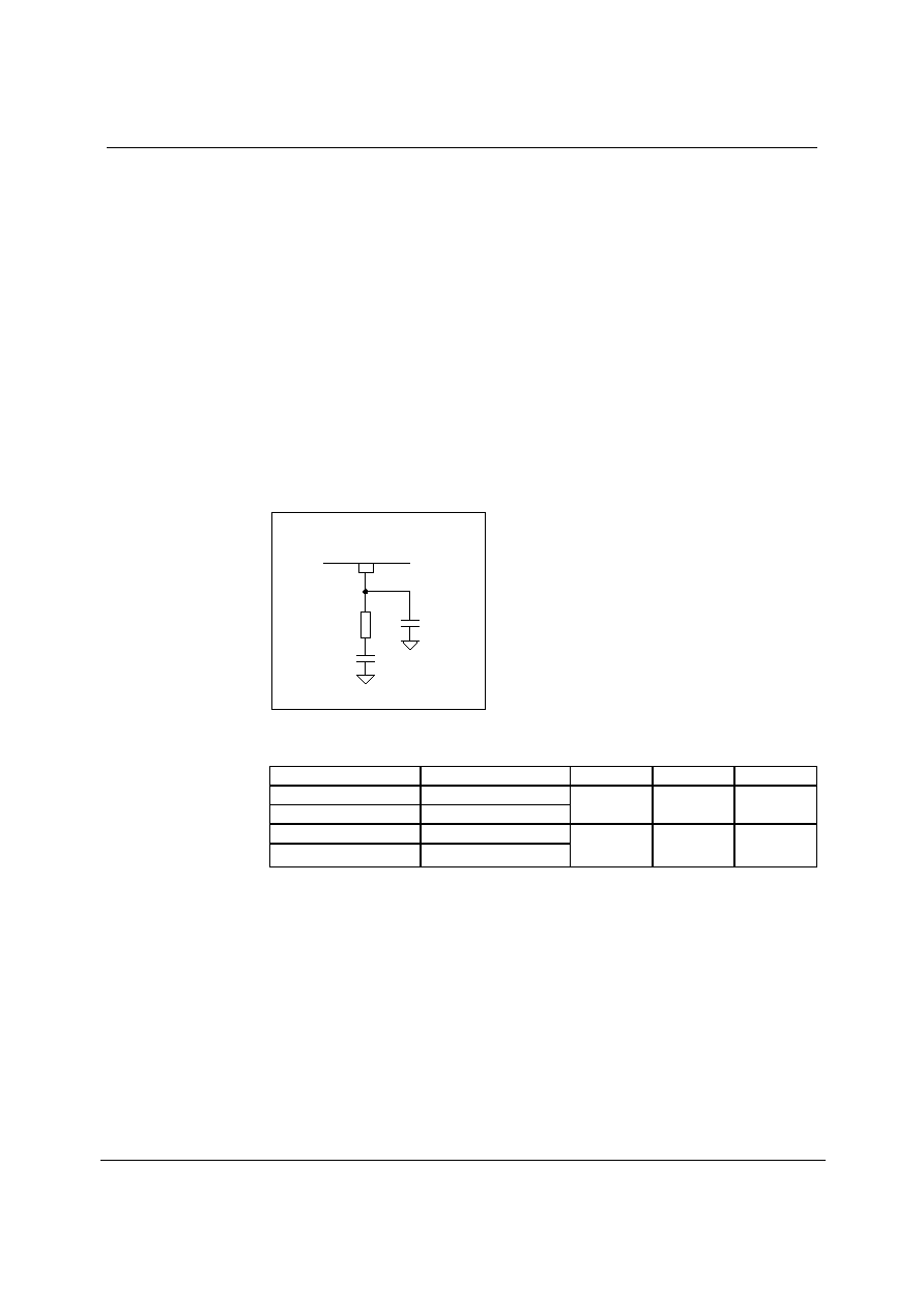
CLOCKS
PLL (LPF)
The VCO (Voltage Controlled Oscillator) can be stopped if PLLOPR is set. Synchronization to
frequencies from 32kHz to 192kHz and RMCK of 4MHz to 25MHz can be selected.
The PLL clock frequency is selected with PLLSEL. For systems with an input data sampling
frequency of 105kHz or lower, the initial setting of 512fs is recommended. Since the system clock
RMCK output initial value is set to 1/2 of PLLSEL, the RMCK output is 256fs when a PLL clock
frequency of 512fs is used.
For systems with an input data sampling frequency higher than 105kHz, the PLL clock frequency
should be set to 256fs. RMCK will be 128fs if PRSEL0 is set to 1 and the same initial output setting
(i.e. 256fs) is used,
LPF is a PLL loop filter pin. Resistances and capacitances should be selected in accordance with
the frequency of the PLLSEL system clock. The PLLSEL setting should be set prior to bi-phase data
input since PLLSEL switching involves a change in LPF loop filter constant.
C
1
C
0
R
0
LPF
Figure 5 Loop Filter Configuration
PLLCK1
PLLCK0
R0
C0
C1
0
0
0
1
150
0.047�F
0.0068�F
1
0
1
1
220
0.068�F
0.0047�F
Table 6 Loop Filter Component Values

Product Preview
WM8802
w
PP Rev 1.0 May 2003
13
DEMODULATION FUNCTION WITHOUT USING PLL (TMCK)
The WM8802 has a function to process input bi-phase data using an external clock (external
synchronization function). In normal demodulation processing, the clock is generated in
synchronization with data by the built-in PLL; the data processing is performed using this clock. It is
possible to perform data processing by supplying a data synchronized clock instead of the clock
generated by the PLL via an independent transmission path.
The demodulation function can be used to set external synchronization function without using the
PLL by EXSYNC. PLLSEL should be set to 256fs and PRSEL0 should be set to 1 (setting frequency
to 1/1). The 256fs clock should then be synchronized with the input data to TMCK. As a result of
these settings, the same operation occurs as PLL demodulation processing with a 256fs clock. LPF
should remain unconnected as no loop filter is required.
The external synchronization function settings should be completed prior to bi-phase data input
(paying attention to the bandwidth of clock transmission path).
A high-precision clock system using an external PLL can also be configured by using the external
synchronization function.
OSCILLATION AMPLIFIERS (XIN, XOUT, MCK)
The WM8802 features a built-in oscillation amplifier. An oscillation circuit can be configured by
connecting a crystal resonator, feedback resistor and load capacitance across XIN and XOUT. When
connecting a crystal resonator, use a fundamental crystal resonator. Note that the load capacitance
depends on the crystal resonator characteristics.
The output of an external clock supply source should be connected to XIN if the built-in oscillation
amplifier is not used as the clock source. In this configuration it is not necessary to connect a
feedback resistor between XIN and XOUT.
A 12.288MHz or 24.576MHz clock can be supplied to XIN by setting XINSEL. If input frequency to
XIN changes it is necessary to set FSERR to 1, so that when the input data sampling frequency
changes, the result is not reflected in the error flag. Since the input frequency is then different to the
recommended frequency operation, the encoding result cannot be used for input fs calculations. In
this case, the input fs can be calculated by performing decimal division of the count value (FSDAT)
with 1/2000th of the XIN input frequency. For details, see Micro-controller Interface section.
Since the XIN clock serves as the reference for internal processing, the XINSEL setting should be
completed prior to bi-phase data input.
A clock should be supplied to XIN at the following times:
(1)
Detection of bi-phase data input
(2)
Clock source during PLL unlock
(3)
Input data sampling frequency calculation
(4)
Time definition during input data switching
(5)
External supply clock source (AD converter clock, etc.)
The oscillation amplifier automatically stops when the PLL is locked. However, it can also be set for
continuous operation with AMPOPR set to 1. Setting the continuous operation mode enables input
data detection and input sampling frequency calculation even when the PLL is locked; this has an
effect on the sound quality because the oscillation amplifier and PLL clock coexist.
RERR outputs an error (High) once the PLL is locked if the oscillation amplifier is set to continuous
operation by setting AMPOPR to 1. This occurs because, at the same time that the oscillation
amplifier goes into the operating state, the fs calculation value that is held when operation is stopped,
is reset. This error has no influence on the clock output, but RDATA is muted while this error occurs.
Therefore, the AMPOPR[0:1] setting must be completed either prior to bi-phase data input or during
PLL unlock.
WM8802
Product Preview
w
PP Rev 1.0 May 2003
14
The oscillation amplifier can be stopped if it is unnecessary. When operation is resumed it is
recommended to return to the normal operation after an interval of 10ms or longer to allow the
resonator oscillation to stabilise.
XMCK outputs the XIN clock. The XMCK output settings are performed with XMSEL[0:1]. The XIN
clock can be set to 1/1, 1/2 or muted output.
No clock is needed for XIN when only using the modulation function. In this case, the built-in
oscillation amplifier and frequency divider are used for RMCK, RBCK, and RLRCK clock generation.
Input the crystal resonator frequency across XIN and XOUT (if using only the oscillation amplifier) or
an external clock to XIN. The potential of digital data input pins RX0 to RX6 should be fixed. The DIR
function is stopped using RXOPR and PLLOPR and should not be set at this time. The output clock
may also be muted.
MASTER CLOCK AND CLOCK SOURCE SWITCHING
The RMCK, RBCK, and RLRCK, and the SBCK and SLRCK (see below) clock sources can be
selected from the following three master clocks.
(1)
PLL source
(256fs or 512fs)
(2)
XIN source
(12.288MHz or 24.576MHz)
(3)
TMCK source
(256fs)
Clock source switching can be done in one of two ways, either by setting the R system and the S
system on an interconnected basis or fixing the S system to the XIN source and setting only the R
system. This setting is performed using SELMTD, OCKSEL and RCKSEL.
The clock source is automatically switched between PLL clock and XIN clock by locking/unlocking
the PLL. The continuity of the clock is maintained at this time. However, if switching the clock source
with SELMTD, the continuity of the S system is not maintained.
The clock source can be switched to XIN using OCKSEL and RCKSEL, regardless of the PLL status.
The clock source switch command and clock output of the R and S systems are shown below.
SELMTD
R SYSTEM OUTPUT CLOCK
S SYSTEM OUTPUT CLOCK
0
According to OCKSEL
According to OCKSEL
1
According to RCKSEL
Fixed to XIN source
Table 7 Correspondence between Clock Source Switch Commands and Clock Output Pins
R SYSTEM CLOCK
SOURCE
S SYSTEM CLOCK
SOURCE
SELMTD
OCKSEL
RCKSEL
Locked
Unlocked
Locked
Unlocked
0
X
PLL
XIN
PLL
XIN
0
1
X
XIN
XIN
XIN
XIN
X
0
PLL
XIN
XIN
XIN
1
X
1
XIN
XIN
XIN
XIN
Table 8 Relationship between Clock Source Switch Commands and
Clock Sources when PLL Locked/Unlocked
The TMCK source is selected using EXSYNC. This setting results in the same operation as when
256fs is set with the PLL source (i.e. PLLSEL set to 256fs).
The various clocks are output with the TMCK source as the master clock and the PLL clock status is
output if data synchronised with TMCK is input. The XIN source is switched with OCKSEL and
RCKSEL. When the TMCK source is not supplied or the input data is not synchronized, the source is
switched to the XIN source; this is similar to the PLL source unlocked status.
The PLL status can always be monitored with RERR even after the XIN source is switched. The
processed information can also be read with the micro-controller interface regardless of the PLL
status.
Product Preview
WM8802
w
PP Rev 1.0 May 2003
15
When the PLL changes from locked to unlocked status, the timing for switching the clock from the
PLL source to the XIN source can be changed with XTWT[0:1]. It is recommended to use these
commands if noise occurs during clock switching.
CAUTIONS ON SWITCHING CLOCK SOURCEWHILEPLL IS LOCKED
Clock continuity is maintained when switching the clock to the XIN source with SELMTD, OCKSEL,
and RCKSEL. RERR outputs an error (High) when the oscillation amplifier is stopped while the PLL
is locked (initial setting). The oscillation amplifier goes into the operating state at the same time that
the clock is switched to the XIN source and calculation of the input fs (sampling frequency) resumes.
The previous fs calculation value is then reset. The processing performs as if the fs value had
changed compared to the newly calculated fs value.
The following settings must be performed in order to switch the clock source with SELMTD, OCKSEL
and RCKSEL while PLL is locked and maintaining the RERR status.
(1)
Set the oscillation amplifier to the continuous operation mode with AMPOPR[0:1].
(2)
Set with FSERR the mode for not reflecting fs changes to the error flag.
By performing one of the above settings, it is possible to control the RERR change status when
switching the clock source with SELMTD, OCKSEL and RCKSEL.
When switching the clock source to XIN (oscillation amplifier stopped and PLL locked), the output
clock is output after the oscillation amplifier starts operating. When switching the clock source from
XIN to PLL the clock continuity is maintained.
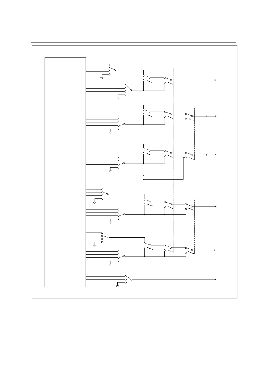
MASTER CLOCK BLOCK DIAGRAM (TMCK, XIN, XOUT, RMCK, XMCK)
The relationships between the three master clocks, switching and the frequency division function are
shown below.
The contents in the square brackets [
] of the switch function blocks correspond to the write
command names.
Lock/Unlock switching is automatically performed through PLL locking/unlocking.
PLL
1/N
(256fs or 512fs)
Selected Biphase
TMCK (I) 256fs only
XIN (I)
XOUT (O)
RMCK (O)
XMCK (O)
[EXSYNC]
[RCKSEL]
[PLLOPR]
[PLLSEL]
[PRSEL1]
[XRSEL1]
[XINSEL]
[XMSEL1]
[AMPOPR1]
(N=1, 2)
Lock /Unlock
1/N
(N=1, 2)
1/N
(N=1, 2, 4)
1/N
(N=1, 2, 4)
[OCKSEL]
[XMSEL0]
[XRSEL0]
[PRSEL0]
[SELMTD]
[AMPOPR0]
Figure 6 Master Clock Block Diagram

WM8802
Product Preview
w
PP Rev 1.0 May 2003
16
OUTPUT CLOCKS (RMCK, RBCK, RLRCK, SBCK, SLRCK)
The WM8802 features two clock systems in order to supply the various clocks for the A/D converter,
DSP and other peripheral devices.
The clock output settings for the R and S systems are set using PRSEL[0:1], XRSEL[0:1],
XRBCK[0:1], XRLRCK[0:1], PSBCK[0:1], PSLRCK[0:1], XSBCK[0:1], and XSLRCK[0:1].
(a)
Setting range for clock output pins when using the PLL source
(1)
RMCK: 1/1, 1/2, and 1/4 of 512fs or 256fs
(2)
RBCK: 64fs output
(3)
RLRCK: fs output
(4)
SBCK: 128fs, 64fs, and 32fs
(5)
SLRCK: 2fs, fs, and fs/2
(b)
Setting range for clock output pins when using the XIN source
(1)
RMCK: 1/1, 1/2, and 1/4 of 12.288MHz or 24.576MHz
(2)
RBCK: 12.288MHz, 6.144MHz, and 3.072MHz
(3)
SBCK: 12.288MHz, 6.144MHz, and 3.072MHz
(4)
RLRCK: 192kHz, 96kHz, and 48kHz
(5)
SLRCK: 192kHz, 96kHz, and 48kHz
The polarity of RBCK, RLRCK, SBCK and SLRCK can be reversed with RBCKP, RLRCKP, SBCKP
and SLRCKP.
Clock switching is processed on the rising edge of the RLRCK output after the falling edge of micro-
controller interface CE.
PLL SOURCE
TMCK
SOURCE
XIN SOURCE
OUTPUT PIN NAME
512fs
256fs
256fs
12.288MHz
24.576MHz
512fs
256fs
256fs
12.288MHz
24.576MHz
256fs
128fs
128fs
6.144MHz
12.288MHz
RMCK
128fs
64fs
64fs
3.072MHz
6.144MHz
12.288MHz
64fs
6.144MHz
RBCK
3.072MHz
192kHz
fs
96kHz
RLRCK
48kHz
128fs
12.288MHz
64fs
6.144MHz
SBCK
32fs
3.072MHz
2fs
192kHz
fs
96kHz
SLRCK
fs/2
48kHz
Table 9 Output Clock Frequencies (Bold Items = Initial Settings)

Product Preview
WM8802
w
PP Rev 1.0 May 2003
17
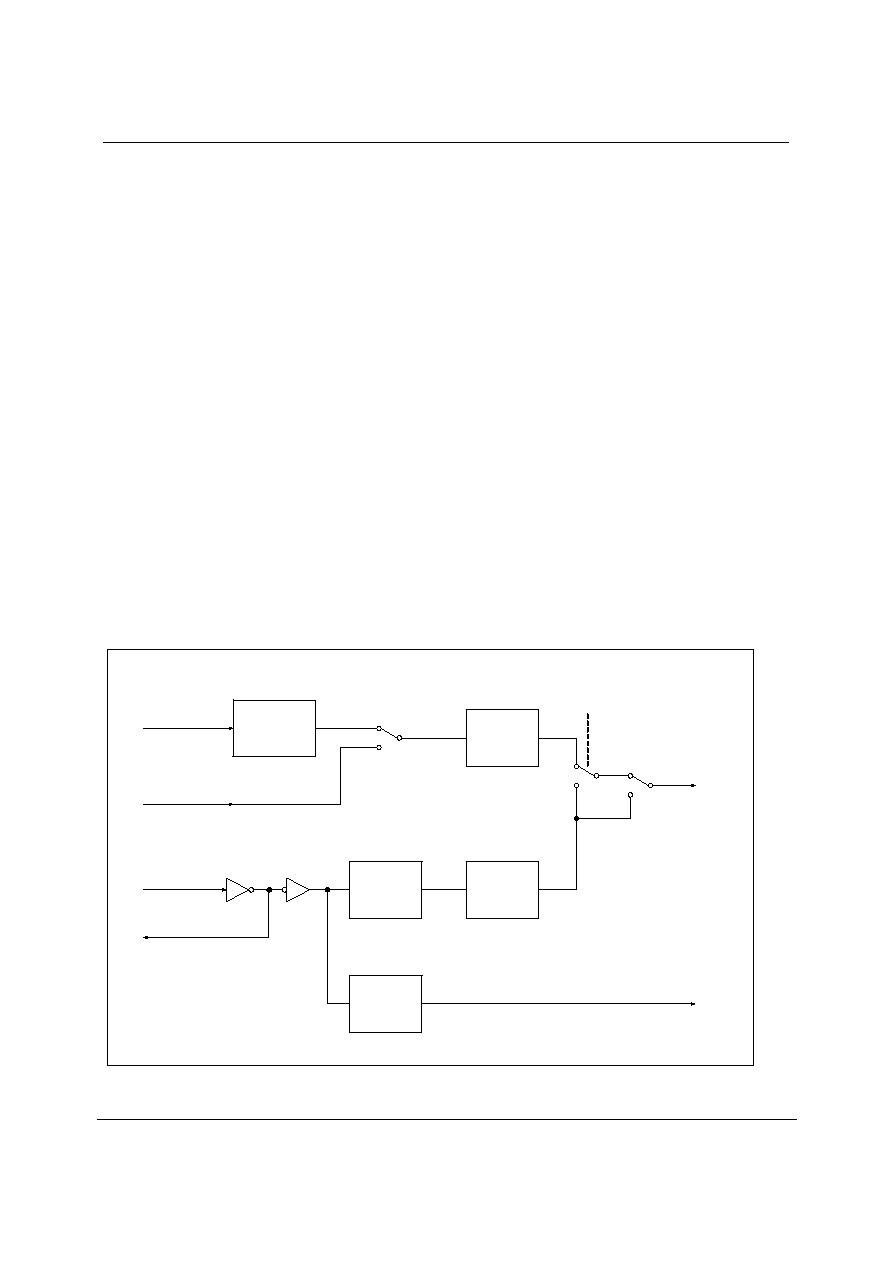
OUTPUT CLOCKS BLOCK DIAGRAM (RMCK, RBCK, RLRCK, SBCK, SLRCK,
XMCK)
The relationships between the output clock and switch function are shown below.
Master Clock Generator in the figure indicates the PLL source, TMCK source or the XIN source.
The contents in the square brackets [
] of the switch function blocks correspond to the write
command names.
The broken lines connecting the switches indicate coordinated switching.
Lock/Unlock switching is automatically performed through PLL locking/unlocking.
Master/slave switching is done through demodulation function master/slave function switching.
WM8802
Product Preview
w
PP Rev 1.0 May 2003
18
Master Clock
Generator
SBCK (O)
SLRCK (O)
XMCK (O)
XTAL Source
PLL Source
RMCK (O)
512fs / 256fs
256fs / 128fs
128fs / 64fs
MUTE
2fs
fs
fs/2
MUTE
RBCK (I/O)
RLRCK (I/O)
to internal circuits
PLL 64fs
PLL fs
[RCKSEL] ([SELMTD]=1)
Master / Slave
128fs
64fs
32fs
MUTE
12.288MHz / 24.576MHz
6.144MHz / 12.288MHz
MUTE
Lock / Unlock
[PRSEL]
[XRSEL]
[PSBCK]
[PSLRCK]
[XSLRCK]
[XMSEL]
[SELMTD]
12.288MHz / 24.576MHz
6.144MHz / 12.288MHz
3.072MHz / 6.144MHz
MUTE
[XRBCK]
[XRLRCK]
12.288MHz
6.144MHz
3.072MHz
MUTE
[XSBCK]
192kHz
96kHz
48kHz
MUTE
PLL
XIN
PLL
XIN
PLL
XIN
PLL
XIN
PLL
XIN
XIN
192kHz
96kHz
48kHz
MUTE
12.288MHz
6.144MHz
3.072MHz
MUTE
12.288MHz or 24.576MHz
256fs or 512fs
TMCK Source
256fs
[OCKSEL] ([SELMTD]=0)
Figure 7 Clock Output Block Diagram
Product Preview
WM8802
w
PP Rev 1.0 May 2003
19
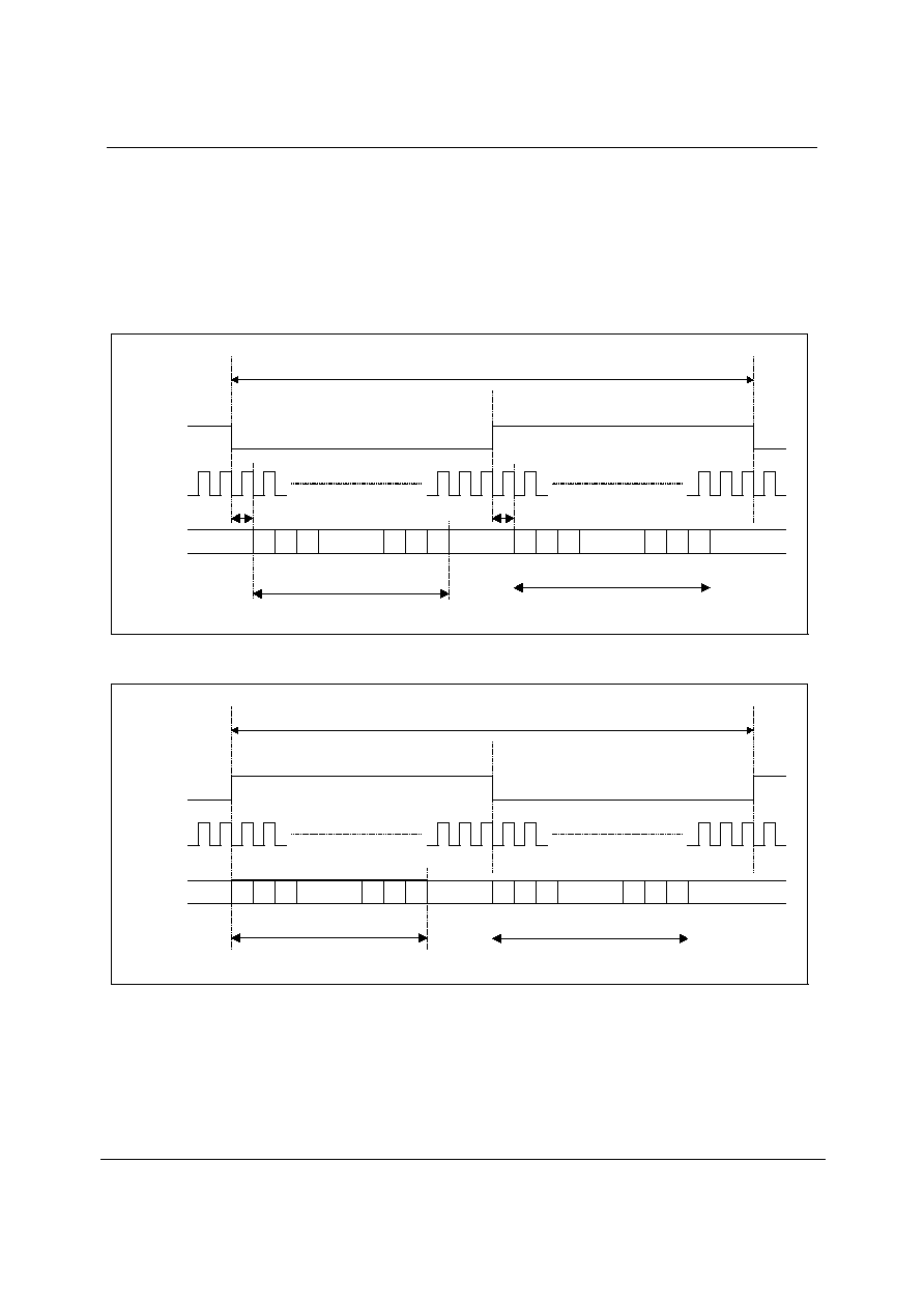
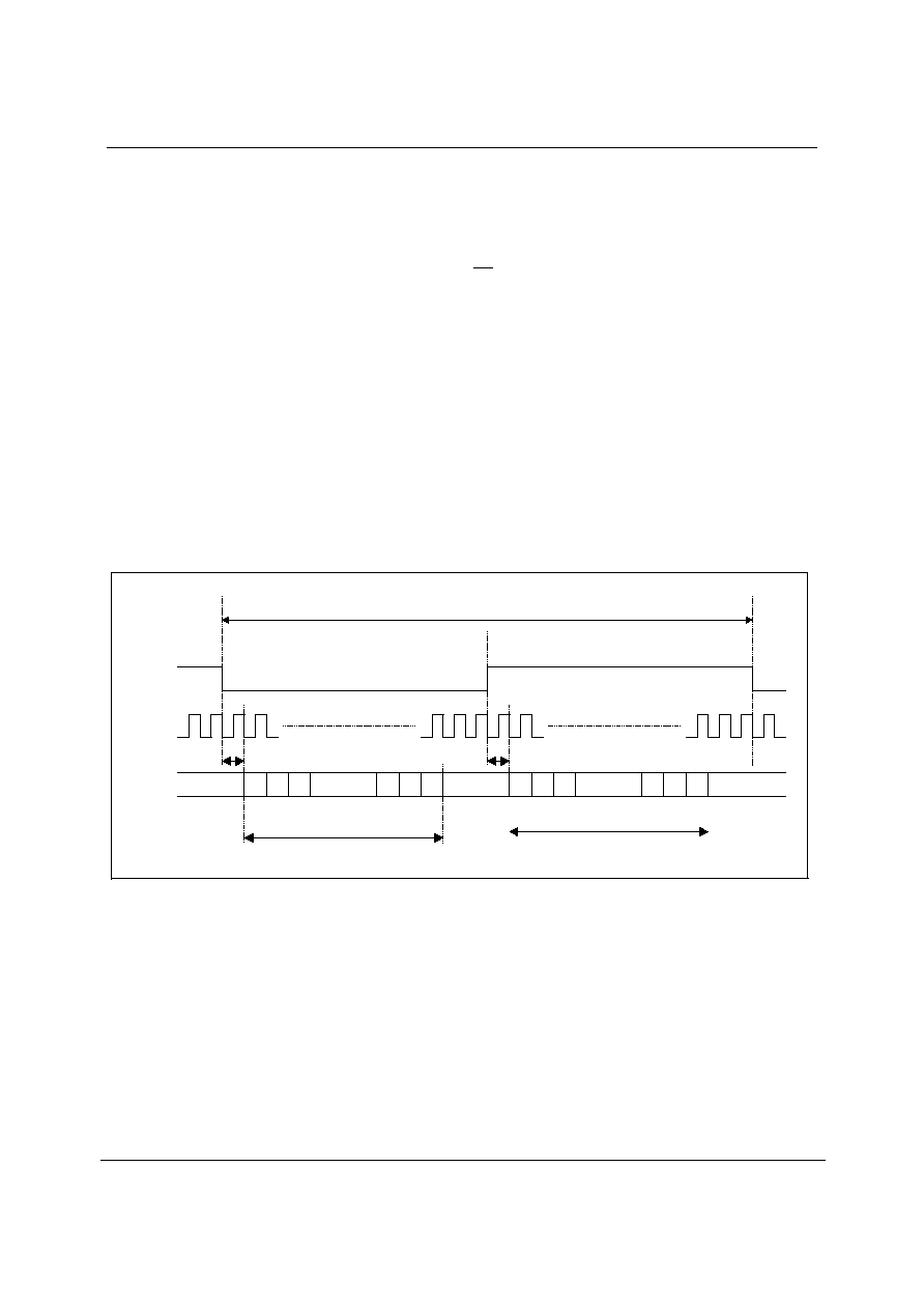
CLOCK SWITCH TRANSITION SIGNAL OUTPUT ( CKST )
CKST outputs Low when the output clock changes during PLL lock/unlock.
In the lock-in stage (PLL locked following the detection of input data) the CKST Low pulse falls at
the word clock edge generated from the XIN clock. The CKST Low pulse rises at the same timing as
RERR following the lapse of a given period.
In the unlock stage, the CKST Low pulse falls at the same timing as the PLL lock detection signal
RERR and rises following a given number of word clocks generated from the XIN clock.
The PLL lock status change and clock change timing is detected by the rising and falling edges of
the CKST Low pulse.
RERR
RMCK
VCO Clock
XTAL Clock
Locked status
RX0 to RX6
(a) Lock-in stage
45 ms to 300 ms
Same timing as
RERR
After PLL lock
Digital Data
Lock
Unlock
CKST
RERR
RMCK
VCO Clock
XTAL Clock
Locked status
RX0 to RX6
(b) Unlock stage
Same timing as RERR
Digital Data
Unlock
Lock
CKST
0.6 ms to 6.4 ms
Figure 8 Clock Switch Timing

WM8802
Product Preview
w
PP Rev 1.0 May 2003
20
BI-PHASESIGNAL INPUT / OUTPUT
BI-PHASE SIGNAL INPUT RECEPTION RANGE
The input data reception range depends on the PLL lock frequency setting set by PLLSEL. The
relationship between this setting and the guaranteed reception range is shown below.
PLL OUTPUT CLOCK SETTING
INPUT DATA RECEPTION RANGE
512fs (PLLSEL = 0)
28kHz to 105kHz
256fs (PLLSEL = 1)
28kHz to 195kHz
Table 10 Relationship Between PLL Output Clock Setting and Reception Range
(FSLIM[0:1] = 0)
The fs reception range for input data within the above PLL output clock setting range can be
controlled. This setting is performed using FSLIM[0:1]. When this function is used, input data that
exceeds the setting range is considered as an error and the clock source is automatically switched to
the XIN source. The RDATA output data then depends on the RDTSEL setting.
BI-PHASESIGNAL INPUT/OUTPUT PINS (RX0 TO RX6, RXOUT)
There are 7 digital data input pins. Data modulated with the modulation function can also be
selected, therefore selection from a total of 8 signals is possible. However, the pins that can be
selected are restricted by the following conditions:
1.
The six pins RX0 and RX2 to RX6 are TTL level input pins with 5V input level tolerable.
2.
RX1 is a coaxial-compatible input pin with built-in amplifier that can receive up to 200mVp-p
data.
The demodulation input and RXOUT output signals can also be selected independently.
1.
The demodulation data is selected with RISEL[0:2].
2.
The RXOUT output data is selected with ROSEL[0:2].
RXOUT can be muted with RXOFF. Muting is recommended when not using RXOUT in order to
reduce clock jitter.
The data input status can be monitored with the RXMON setting. The status of each data input pin is
stored in CCB address 0xEA and output registers DO0 to DO7. Since this function uses the XIN
clock, the oscillation amplifier must be set to the continuous operation mode when RXMON is set.
Demodulation input pin switching can be performed during PLL unlock using the ULSEL setting. As a
result, data switching can be accurately communicated to peripheral devices.
The interval from pin switching through RISEL[0:2] until data is received is about 250
�
s to 350
�
s.
This function also requires that the oscillation amplifier is set to the continuous operation mode.
Input pin selection
Internal supply signal
RX0
RX2
RX3
RX1
RX0
RX2
RX3
RX1
250
�
�
�
�
s to 350
�
�
�
�
s
Figure 9 Input Pin Selection Processing via PLL Unlock
Product Preview
WM8802
w
PP Rev 1.0 May 2003
21
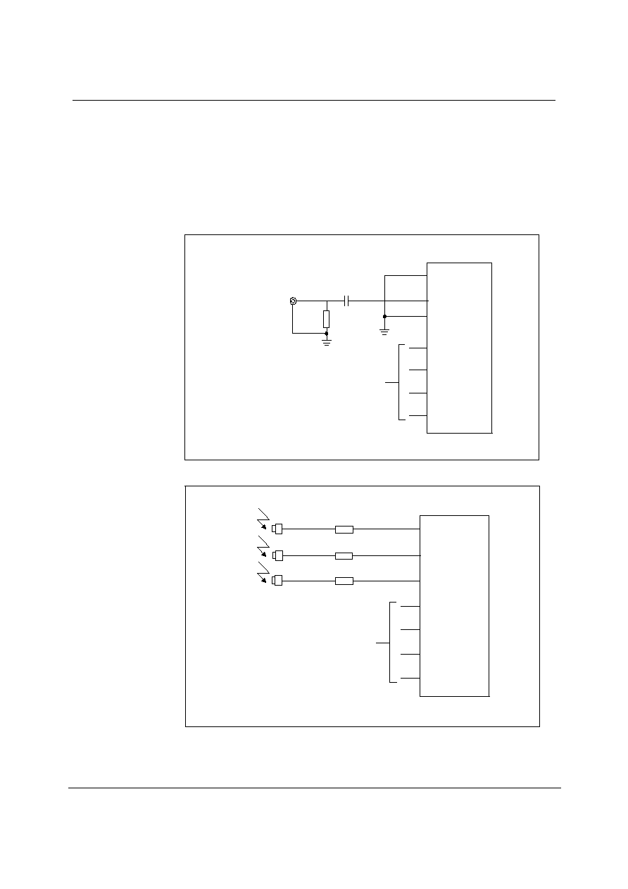
BI-PHASESIGNAL INPUT CIRCUITS (RX0, RX1, RX2)
If RX1, which has a built-in amplifier, is used as a coaxial input signal corruption may occur due to
the influence of the adjacent RX0 and RX2 input pins. RX0 and RX2 should be fixed to Low to
prevent them from influencing RX1.
The input signal to RX1 is temporarily open if RX1 is selected. The RX0 and RX2 potential must be
fixed due to coupling effects. In this case, 5 bi-phase signal input pins can be selected; RX1 and RX3
to RX 6.
If the input signal to RX1 is absolutely fixed to either High or Low then all 7 input pins can be used.
RX0
RX1
RX2
RX3
RX4
RX5
RX6
WM8802
Other inputs
0.1
�
F
75
Coaxial
Figure 10 Bi-Phase Signal Input Circuits � Coaxial Input Circuit
RX0
RX1
RX2
RX3
RX4
RX5
RX6
WM8802
Other inputs
100
Optical
100
100
Figure 11 Bi-Phase Signal Input Circuits � Optical Input Circuit
WM8802
Product Preview
w
PP Rev 1.0 May 2003
22
SERIAL AUDIO DATA INPUT/OUTPUT
OUTPUT DATA FORMAT (RDATA)
The output format is set with OFSEL[0:2].
I
2
S is the initial output format setting.
Right Justified outputs are only valid in master mode.
Output data is output in synchronization with the RLRCK edge immediately after the RERR output
becomes Low.
LEFT
CHANNEL
RIGHT
CHANNEL
RLRCK (0)
RBCK (0)
RDATA (0)
1/fs
n
3
2
1
n-2 n-1
LSB
MSB
n
3
2
1
n-2 n-1
LSB
MSB
1 BCLK
1 BCLK
16 to 24 bits
16 to 24 bits
Figure 12 Data Output Timing � I2S
LEFT
CHANNEL
RIGHT
CHANNEL
RLRCK (0)
RBCK (0)
RDATA (0)
1/fs
n
3
2
1
n-2 n-1
LSB
MSB
n
3
2
1
n-2 n-1
LSB
MSB
16 to 24 bits
16 to 24 bits
Figure 13 Data Output Timing � Left Justified
Product Preview
WM8802
w
PP Rev 1.0 May 2003
23
LEFT
CHANNEL
RIGHT
CHANNEL
RLRCK (0)
RBCK (0)
RDATA (0)
1/fs
n
3
2
1
n-2 n-1
LSB
MSB
n
3
2
1
n-2 n-1
LSB
MSB
16,20,24 bits
16,20,24 bits
Figure 14 Data Output Timing � Right Justified
SERIAL AUDIO DATA INPUT FORMAT (SDIN)
SDIN is a 24 bit serial digital audio data input pin.
The format of the serial audio data input to SDIN is the same as the demodulation data output
format.
LEFT
CHANNEL
RIGHT
CHANNEL
RLRCK (0)
RBCK (0)
RDATA (0)
1/fs
MSB
16 to 24 bits
16 to 24 bits
SDIN (1)
n
3
2
1
n-2 n-1
LSB
n
3
2
1
n-2 n-1
LSB
MSB
1 BCLK
1 BCLK
n
3
2
1
n-2 n-1
LSB
n
3
2
1
n-2 n-1
LSB
MSB
1 BCLK
1 BCLK
Figure 15 Serial Audio Data Input Timing - I2S Data Input
WM8802
Product Preview
w
PP Rev 1.0 May 2003
24
LEFT
CHANNEL
RIGHT
CHANNEL
RLRCK (0)
RBCK (0)
1/fs
LSB
MSB
16 to 24 bits
16 to 24 bits
RDATA (0)
n
3
2
1
n-2 n-1
LSB
MSB
n
3
2
1
n-2 n-1
SDIN (1)
n
3
2
1
n-2 n-1
LSB
MSB
n
3
2
1
n-2 n-1
Figure 16 Serial Audio Data Input Timing � Left Justified
LEFT
CHANNEL
RIGHT
CHANNEL
RLRCK (0)
RBCK (0)
1/fs
LSB
MSB
LSB
MSB
16,20,24 bits
16,20,24 bits
RDATA (0)
n
3
2
1
n-2 n-1
n
3
2
1
n-2 n-1
SDIN (1)
n
3
2
1
n-2 n-1
n
3
2
1
n-2 n-1
Figure 17 Serial Audio Data Input Timing � Right Justified

Product Preview
WM8802
w
PP Rev 1.0 May 2003
25
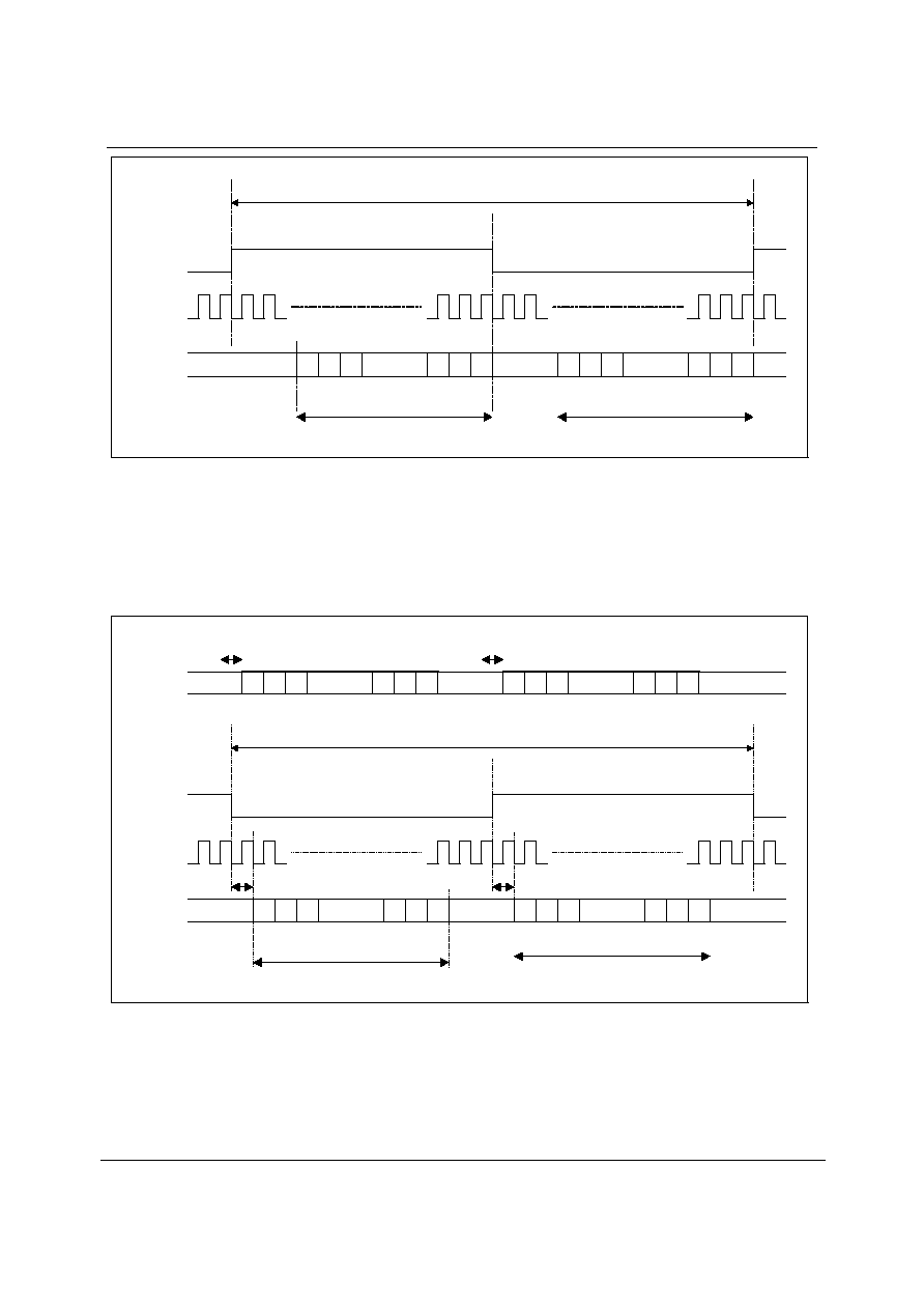
OUTPUT DATA SWITCHING (SDIN, RDATA)
RDATA demodulation data is output when the PLL is locked and the SDIN input is selected This
switching is automatically performed according to the locked/unlocked status of the PLL. For details,
see the timing charts below.
Switch to a clock source synchronized to the SDIN data when SDIN input data is selected.
The SDIN input data can be output to RDATA regardless of the locked/unlocked status of the PLL
using RDTSTA setting.
The RDATA output data can be forcibly muted using the RDTMUT setting.
The PLL continues operating when the clock source is set to XIN using OCKSEL and RCKSEL as
long as its operation is not stopped using PLLOPR. The PLL status is continuously output from
RERR as long as error output is not forcibly set with RESTA. The processed information can also be
read with the micro-controller interface regardless of the PLL status.
RERR
(a) Lock-in stage
RDATA
UNLOCK
LOCK
(b) Unlock stage
RERR
RDATA
PLL locked status
LOCK
UNLOCK
SDIN data
Muted
Demodulation data
SDIN data
Demodulation data
Muted
PLL locked status
CKST
CKST
Figure 18 RDATA Output Data Switch Timing Chart
DATA BLOCK DIAGRAM (RX0 TO RX6, TX0, RXOUT, TDATA, RDATA, SDIN)
The RDATA output data is switched to SDIN input data using RDTSEL.
The SDIN input data can be input to the modulation function using TDTSEL.
The modulation output is an input to the Input Switch Multiplexer and can be output from RXOUT. It
is possible to use a signal that has been digitized with an A/D converter for digital recording output,
etc. using this function.

WM8802
Product Preview
w
PP Rev 1.0 May 2003
26
MUX
(8in / 2out)
DIR
RX0
RX1
RX2
RX3
RX4
RX5
RX6
RDATA
RXOUT
TXO
DIT
TDATA
SDIN
[RDTSEL]
[TDTSEL]
Figure 19 Data Block Diagram
CALCULATION OF INPUT DATA SAMPLING FREQUENCY
The input data sampling frequency is calculated using the XIN clock.
When the oscillation amplifier automatically stops during PLL lock, the input data sampling frequency
is calculated during the RERR error period. The calculation is completed at the same time that the
oscillation amplifier stops. The value remains unchanged until the PLL becomes unlocked.
In the mode where the oscillation amplifier operates continuously, calculation processing is
performed continuously The calculation results (which follows the input data) can be read even if
sampling rate is changed within the PLL capture range, but only for a signal where channel status
sampling information does not change,.
The calculation result can be read from CCB address 0xEB and output to registers DO4 to DO7 and
DO8 to DO15. Registers DO4 through DO7 hold the encoded result, while DO8 through DO15 hold
the calculation value. The sampling frequencies that can be calculated are greater than 24kHz as the
calculation count value is output in 8-bit units. For details, see section Micro-controller Interface.
ERROR OUTPUT PROCESSING
LOCK ERROR, DATA ERROR OUTPUT (RERR)
An error flag RERR is output when a PLL lock error or a data error occurs.
Non-PCM data reception can be treated as an error with the RESEL setting.
The RERR output conditions are set using RESTA. Since the PLL status can be output at any time,
the PLL status can be monitored even when the clock source is XIN.

Product Preview
WM8802
w
PP Rev 1.0 May 2003
27
PLL LOCK ERROR
The PLL becomes unlocked for input data that has lost bi-phase modulation regularity or input data
where preambles B, M, and Wcannot be detected.
RERR goes High during the occurrence of a PLL lock error and returns to Low when data
demodulation returns to normal. High is maintained between 45ms and 300ms.
The rising and falling edges of RERR are synchronized with RLRCK.
INPUT DATA PARITY ERROR
Input parity errors are detected if there are an odd number of parity bits in input data.
RERR goes High indicating that the PLL is locked if an input parity error occurs 9 or more times in
succession, It returns to Low after being High for between 45ms and 300ms.
The error flag output format, for when an input parity error is output 8 times in succession, can be
selected using REDER.
OTHER ERRORS
The channel status bits 24 to 27 (sampling frequency) are always read and the data of the previous
block is compared with the current data, even if RERR goes Low. The input data sampling frequency
is also calculated from the fs clock extracted from the input data and fs calculation value comparison
is performed as described above. RERR is instantly made High if a difference is detected, and the
same processing as for PLL lock errors is performed.
The PLL causes a lock error when the sampling frequency changes as described above. FSERR can
be set to support sources with a variable sampling frequency (for example a CD player with a
variable pitch function). No error flag is output if the sampling frequency variation falls within the PLL
capture range while using FSERR.
For input data within the reception range, FSERR prevents fs calculation results from being reflected
in the error flag that is set using FSLIM[0:1]. RERR goes Low if the PLL status changes to the locked
status.
RERR changes to a High output upon detection of non-PCM data input if RESEL is set. The PLL
locked status and various output clocks continue to be output according to the input data but the
output data is muted.
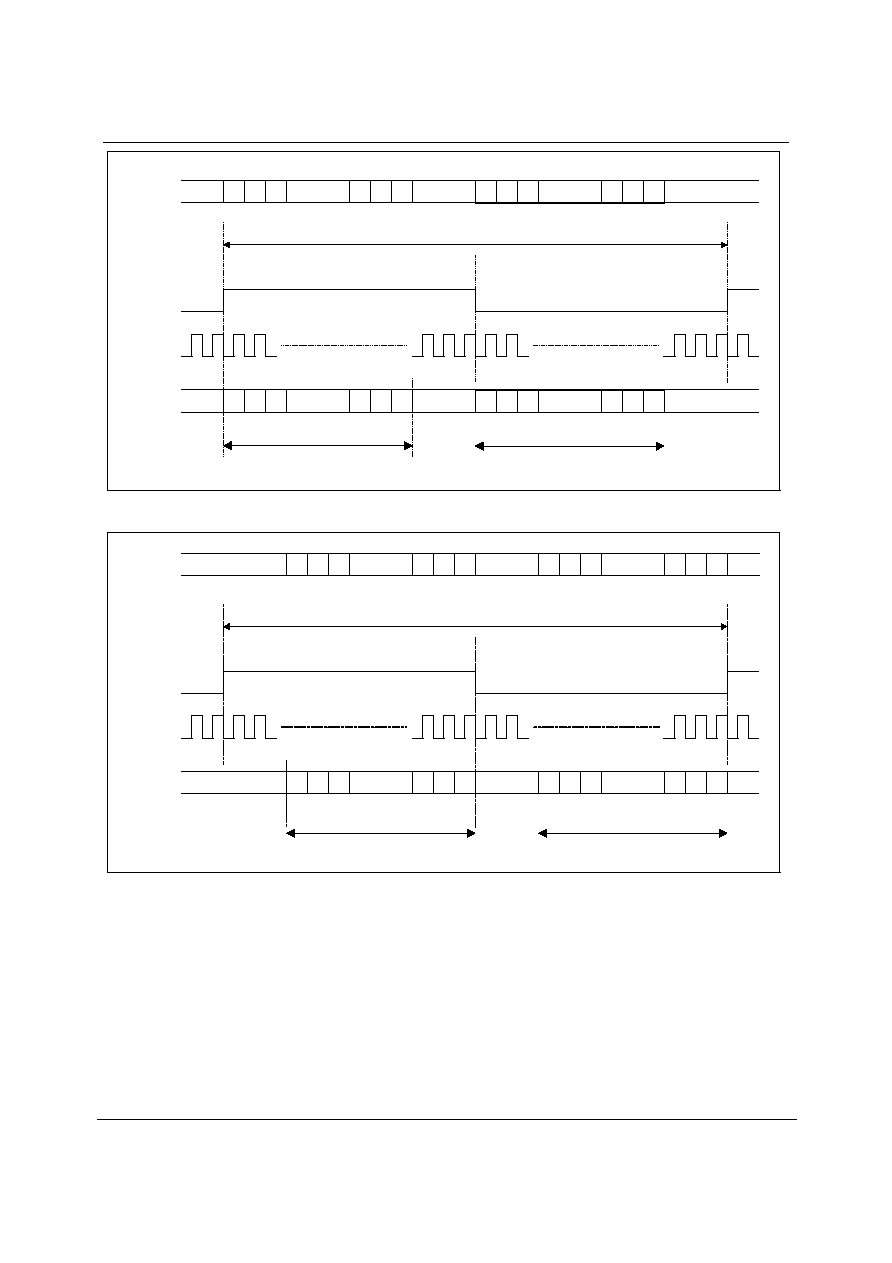
DATA PROCESSING UPON ERROR OCCURRENCE (LOCK ERROR, PARITY
ERROR)
The data processing after the occurrence of an error is described below. If 8 or fewer input parity
errors occur in succession transfer data is replaced by the data saved to L-ch and R-ch in the
previous frame of PCM audio data. The error data is output as it is if the transfer data is non-PCM
data. Non-PCM data is based on data detected prior to occurrence of an input parity error when bit 1
of the channel status goes High.
Output data is muted upon occurrence of a PLL lock error or when a parity error occurs 9 or more
times in succession.
For the channel status, the data of the previous block is held in 1-bit units when a parity error occurs.
WM8802
Product Preview
w
PP Rev 1.0 May 2003
28
DATA
PLL LOCK
ERROR
INPUT PARITY
ERROR (A)
INPUT PARITY
ERROR (B)
INPUT PARITY
ERROR (C)
RDATA output
Low
Low
Previous value data
Output
fs calculation result
Low
Output
Output
Output
Channel status
Low
Low
Previous value data
Previous value data
Validity flag
Low
Low
Output
Output
User data
Low
Low
Output
Output
Table 11 Data Processing upon Error Occurrence
Notes:
1.
Input parity error (A): Occurs 9 or more times in succession
2.
Input parity error (B): Occurs 8 or fewer times in succession, in case of audio data
3.
Input parity error (C): Occurs 8 or fewer times in succession, in case of non-PCM burst data
Figure 20 shows an example of data processing upon occurrence of a parity error.
RERR
RDATA
R-ch
Previous data value
Input Data
RLRCK
An error occurs a single time
Muted after 9 or more
consecutive errors
L-ch R-ch ....
Previous data value
R-2
L-2
R-0
L-1
R-0
L-0
L-2 R-2 L-2 R-2 L-2 R-2 L-2 R-2
L-4
R-3
L-3
R-2
L-2
R-1
R-4 L-5 R-5 L-6 R-6 L-7 R-7 L-8 R-8
L-1
Figure 20 Data Processing Upon Parity Error Occurrence
PROCESSING DURING ERROR RECOVERY
PLL becomes locked and data demodulation begins when preambles B, M and Ware detected.
RDATA output data is output from the RLRCK edge after RERR goes Low.
Product Preview
WM8802
w
PP Rev 1.0 May 2003
29
RDATA
Output starts from the RLRCK edge immediately after RERR flag is lowered
RERR
Internal clock signal
RLRCK
Data
45 ms to 300 ms
OK
Figure 21 Internal Lock Signal
CHANNEL STATUS OUTPUT
DATA CATEGORY SPECIFICATION BIT 1 OUTPUT ( AUDIO )
The AUDIO pin outputs bit 1 of the channel status indicating that the input bi-phase data is PCM
audio data. AUDIO status is immediately output upon detection of RERR even during High output.
An output ORed with IEC61937 or the DTS-CD/LD detection flag is also possible with AOSEL.
AUDIO
OUTPUT CONDITIONS
0
PCM audio data (CS bit 1 = Low)
1
Non-audio data (CS bit 1 = High
Table 12 AUDIO Output
EMPHASIS INFORMATION OUTPUT (EMPHA)
The EMPHA pin output indicates that the signal has the presence or absence of 50/15
�
s emphasis
for consumer and broadcast studio.
EMPHA status is immediately output upon detection of RERR even during High output.
EMPHA
OUTPUT CONDITIONS
0
No pre-emphasis
1
50/15
�
s pre-emphasis
Table 13 EMPHA Output

WM8802
Product Preview
w
PP Rev 1.0 May 2003
30
OTHER OUTPUTS
VALIDITY FLAG OUTPUT (VO)
The validity flag can be output from the AUDIO /VO pin by selecting the AUDIO /VO output with
VOSEL.
The validity flags transferred at each sub-frame are output as indicated in the timing diagram below.
VO
OUTPUT CONDITIONS
0
No error (not burst data)
1
Error (May be burst data)
Table 14 VO Output
V-L2
V-R2
V-L3
V-R1
V-L1
L1
L2
L3
R2
R1
RLRCK
RBCK
UO
Figure 22 Validity Flag Output Timing
USER DATA OUTPUT (UO)
User data can be output from the EMPHA/UO pin by selecting the EMPHA/UO output using UOSEL.
The user data transferred at each sub-frame is output as indicated in the following timing diagram.
RLRCK
RBCK
UO
U
U
U
U
U
Figure 23 User Data Output Timing
Product Preview
WM8802
w
PP Rev 1.0 May 2003
31
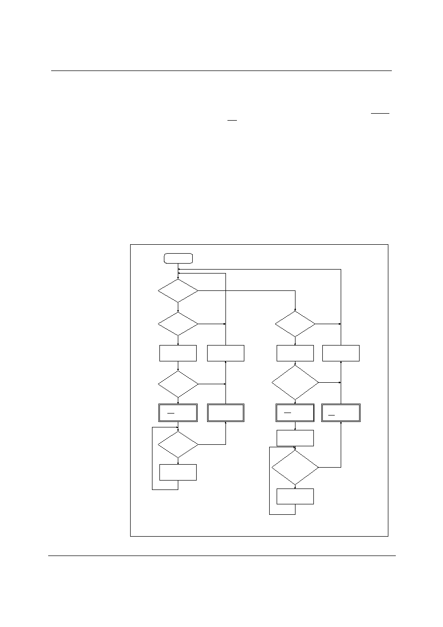
IEC61937, DTS-CD/LD DETECTION FLAG OUTPUT
A function to output IEC61937 and DTS-CD/LD detection flags for non-PCM data is provided.
When the UNPCM non-PCM signal output setting is selected, as well as an indication on the AUDIO
pin, an interrupt signal is output from INT upon detection of an IEC61937 or DTS-CD/LD sync signal.
Non-PCM signal details can be known by reading this information from the output register.
The IEC61937 sync signal is detected and output when channel status bit 1 is non-PCM data ("1").
The IEC61937 sync signal is not output if bit 1 is PCM data ("0").
DTS-CD/LD sync signal detection is done based on the sync pattern and the base frequency. In the
case of DTS-ES data detection, output is performed when the DTS5.1 channel sync signal is
detected and the DTS-ES sync pattern has been verified.
The IEC61937 and DTS-CD/LD detection flags are cleared when fs has changed or upon occurrence
of a PLL lock error or data error.
Since the DTS sync signal is provided within the audio data, digital data with the same code as the
DTS sync signal may in rare cases exist for regular CD/LD records that are not recorded in the DTS
format. Protection using the sync pattern or base frequency is provided so that such data is not
misinterpreted as DTS-CD/LD detection flags. The detection sequence is shown below.
Frame counter
reset
NO
YES
YES
NO
YES
NO
YES
NO
NO
YES
Input data
DTS-CD/LD
SYNC
detection
*
*
DTS-CD/LD
data hold
Frame counter
start
YES
NO
NO
YES
PaPb
detection
Bit 1 detection
Bit 1 = 1
PaPb
detection
during 4096
frames
IEC61937 flag OK
INT lowered
IEC61937
flag
IEC61937 data
hold
*
Depending on the frame count,
the subsequent detection count
is expanded up to x2.
Periodic fluctuation is supported.
Frame count
512, 1024, 2048, 4096
SYNC detection
Frame count hold
x2 count detection
expansion
DTS-CD/LD flag OK
INT lowered
DTS-CD/LD flag
not valid
INT lowered
Frame counter
reset
Frame counter
start
PaPb
detection
during 4096
frames
512
=> 512 or 1024
1024
=> 1024 or 2048
2048
=>
2048 or 4096
4096
=>
4096
1st count
2nd count
Frame count
512, 1024, 2048, 4096
SYNC detection
Figure 24 Detection Flag Output Flowchart
WM8802
Product Preview
w
PP Rev 1.0 May 2003
32
DESCRIPTION OF MODULATION FUNCTION AND GENERAL-PURPOSE I/OS
MODULATION FUNCTION USAGEMETHOD
INITIAL SETTING
The modulation function and general-purpose I/O port function cannot be used simultaneously
because they share the same pins. INT should be pulled down with a 10k
resistor to select the
modulation function. For the setting method, see page 10.
In the initial setting, the modulation function is stopped. The modulation function can be set using
TXOPR.
DATA OUTPUT (TMCK, TBCK, TLRCK, TDATA, TXO)
Bi-phase modulated data is output from TXO by inputting a 256fs clock to TMCK, 64fs clock to
TBCK, fs clock to TLRCK and audio data to TDATA.
The polarity of the TLRCK clock is set using TXLRP.
Input data can be modulated in the sampling range of 32kHz to 192kHz, TMCK rate of 4MHz to
25MHz and up to 24 bit data.
The initial value for the input data format is I
2
S. Switching to Left Justified format is set using TXDFS.
For the channel status, the first 48 bits of data can be written with the micro-controller interface.
TXO is fixed to Low by setting TXOPR to Stop.
LEFT
CHANNEL
RIGHT
CHANNEL
TLRCK (I)
TBCK (I)
TDATA (I)
1/fs
n
3
2
1
n-2 n-1
LSB
MSB
n
3
2
1
n-2 n-1
LSB
MSB
1 BCLK
1 BCLK
16 to 24 bits
16 to 24 bits
Figure 25 Data Input Timing � I2S Data Input

Product Preview
WM8802
w
PP Rev 1.0 May 2003
33
LEFT
CHANNEL
RIGHT
CHANNEL
TLRCK (I)
TBCK (I)
TDATA (I)
1/fs
n
3
2
1
n-2 n-1
LSB
MSB
n
3
2
1
n-2 n-1
LSB
MSB
16 to 24 bits
16 to 24 bits
Figure 26 Data Input Timing � Left Justified Data Input
VALIDITY FLAG INPUT (VI)
Validity flags can be input from RX5/VI by switching the RX5/VI input contents with VISEL.
The validity flag write timing is shown below. The validity flag can be written with the micro-controller
interface but port settings have priority.
Writing validity flags with the micro-controller interface is done using VMODE.
RX5/VI
OUTPUT CONDITIONS
0
No error
1
Error
Table 15 RX5/V1 Input
V-L2
V-R2
V-L3
V-R1
V-L1
L1
L2
L3
R2
R1
TLRCK
TBCK
VI
Internal latch signal
Figure 27 Validity Flag Input Timing
WM8802
Product Preview
w
PP Rev 1.0 May 2003
34
USER DATA INPUT (UI)
User data can be input from RX6/UI by switching the RX6/UI input contents using UISEL.
The user data write timing is shown below.
TLRCK
TBCK
UI
U
U
U
U
U
Internal latch signal
Figure 28 User Data Input Timing
MODULATED OUTPUT OF SDIN INPUT DATA
SDIN input data is modulated and can be output from TXO and RXOUT.
The setting to modulate SDIN input data is set using TDTSEL.
A clock should be input to synchronize SDIN to TMCK, TBCK and TLRCK.
Match the SDIN input data format to the setting used during modulation processing.
MONAURAL OUTPUT
It is possible to output the data of only one input data channel at the input rate of fs/2 with
TXMOD[0:1].
This operation maintains the bi-phase modulation regularity but there is no correlation between the
data and preambles.
Channel status write is synchronized with the output rate.
The validity flag and user data are written in frame units. Input the same data to the L and R
channels.
TLRCK
TDATA
TXO [1]
L2
L3
L4
L1
L0
TXO [2]
R2
R3
R4
R1
R0
L1
R1
L2
R2
L3
R3
L4
R4
L5
R5
R0
M
W
M
W
M
W
M
W
M
M
Ln
Rn
Figure 29 Modulation of Data of Single Channel

Product Preview
WM8802
w
PP Rev 1.0 May 2003
35
GENERAL PURPOSE I/O (GPIO0, GPIO1, GPIO2, GPIO3, GPIOEN)
INITIAL SETTINGS
The modulation function and general-purpose parallel I/O's share the same pins and therefore cannot
be used simultaneously. INT should be pulled down with a 10k
resistor to use the general-purpose
I/O's. For the setting method, see page 10.
The general-purpose parallel I/O output function performs parallel conversion of the serial data input
from the micro-controller interface and outputs the resulting data from GPIO0 GPIO1, GPIO2 and
GPIO3. The input function saves the parallel data input to GPIO0, GPIO1, GPIO2, and GPIO3 to
internal registers and reads the contents of these registers with the micro-controller interface.
It is not possible to mix the 4 bit general-purpose I/O's as inputs and outputs at the same time.
Switching between input and output is done using GPIOEN The general-purpose I/Os all become
input pins when GPIOEN is High and all output pins when GPIOEN is Low.
INPUT/OUTPUT SETTINGS
Data handling for general-purpose I/O is performed using the micro-controller interface and
write/read registers.
General-purpose I/O write settings (Micro-controller
Write register
General-purpose I/O output)
1.
Set GPIOEN to Low to output data from general-purpose I/O's.
2.
Set the data to be output to CCB address 0xE8, command address 0x10 and input registers
DI12 to DI15.
3.
During write operation, make sure "0" is written to modulation function setting registers DI8 to
DI11.
4.
The data written to PI0 to PI3 is output from the general-purpose I/O's.
General-purpose I/O read settings (General-purpose I/O input
Read register
Micro-controller)
1.
Set GPIOEN to High to input data to general-purpose I/O's.
2.
The input data is saved to CCB address 0xEB and output registers DO0 to DO3.
3.
Data can be sent to the micro-controller by reading GPO0 to GPO3.

WM8802
Product Preview
w
PP Rev 1.0 May 2003
36
MICRO-CONTROLLER INTERFACE ( INT , CL, CE , DI, DO)
DESCRIPTION OF MICRO-CONTROLLER INTERFACE
INTERRUPT OUTPUT ( INT )
Interrupts are output when a change has occurred in the PLL lock status or output data information.
Interrupt output is determined by the register that selects the interrupt source, the INT pin that
outputs that state transition and the registers that store the interrupt source data.
When INT is set output High, the occurrence of an interrupt will set INT output Low. INT returns
High after interrupt Low as dictated by the INTOPF setting.
INTOPF can be set to hold the Low pulse for a certain period and then clear it (to High) or clear it at
the same time that the output register is read.
The interrupt sources can be selected from among the following items in Table 16. Multiple sources
can be selected at the same time with the contents of CCB address 0xE8 and command address
0x08. INT outputs the result of ORing (addition) the selected interrupt sources.
INT output = (selected source 1) + (selected source 2) + ... + (selected source n)
NO.
COMMAND NAMEDE
SCRIPTION
1
ERROR
Output when RERR pin status has changed
2
INDET
Output when input data pin status has changed (Oscillation
amplifier operation condition)
3
FSCHG
Output when input fs calculation result has changed. (Output
amplifier condition)
4
CSRNW
Output when channel status data of first 48 bits has changed
5
UNPCM
Output when AUDIO pin status has changed
6
PCRNW
Output when burst preamble Pc has been updated
7
SLIPO
Output when data is read twice during slave setting and missing
data is detected
8
EMPF
Output when emphasis information has changed
Table 16 Interrupt Source Setting Contents
The set interrupt source contents are saved to output registers DO8 to DO15 of CCB address 0xEA.
The status of the RERR and AUDIO pins is output when the read registers for source items 1 and 5
are read. Except for source items 1 and 5, other data is saved to the registers upon occurrence of an
interrupt source.
The oscillation amplifier must be set to the continuous operation mode for source items 2 and 3 when
monitoring is performed even while the PLL is locked .
Following the occurrence of an interrupt from INT , the interrupt is cleared at the same time that the
output registers 0xEA is read.
In the interrupt Low pulse output mode the INT pulse width is between 1/2fs and 3/2fs for one
interrupt pulse.
CCB FORMAT
Function settings as well as information writing and reading are performed by the micro-controller
interface.
The data format of the micro-controller interface conforms to Sanyo's original serial bus format
(CCB). Tri-state instead of open-drain is employed for the data output format.
Data input/output is performed following CCB address input. See the input/output timing chart
Product Preview
WM8802
w
PP Rev 1.0 May 2003
37
REGISTER INPUT/OUTPUT
CONTENTS
R/W
CCB
ADDRESS
B0
B1
B2
B3
A0
A1
A2
A3
Function setting data input
write
0xE8
0
0
0
1
0
1
1
1
CS data input
write
0xE9
1
0
0
1
0
1
1
1
Interrupt data output
read
0xEA
0
1
0
1
0
1
1
1
fs data output
read
0xEB
1
1
0
1
0
1
1
1
CS data output
read
0xEC
0
0
1
1
0
1
1
1
Pc data output
read
0xED
1
0
1
1
0
1
1
1
Table 17 Relationship between Register Input/Output Contents and CCB Addresses
DATA WRITEMETHOD
Input is performed in the following sequence: CCB addresses of A0 to A3 and B0 to B3, chip
addresses of DI0 and DI1, command addresses of DI4 to DI7 and data of DI8 to DI15. DI2 and DI3
are reserved for the system and should always be set to "0".
For the chip addresses, DI0 corresponds to CAL (low-order) and DI1 corresponds to CAU (high-
order).
DATA READ METHOD
Read data is output from DO. DO is in the high impedance state when CE is Low and begins
outputting at the rising edge of CE after the register address is recognised. DO then returns to the
high impedance state at the falling edge of CE.
If DO outputs using multiple WM8802 units are to be shared the DO outputs of the WM8802 can be
set to in a high impedance state using DOEN, This will prevent any misreading of registers from an
unselected device.
INPUT/OUTPUT TIMINGS
B0
DI0
....
A3
A2
A1
A0
B3
B2
B1
DI15
DI5
DI4
DI3
DI2
DI1
DI
DO
Hi-Z
CL
CE
Figure 30 Input Timing Chart (Normal, Low Clock)
WM8802
Product Preview
w
PP Rev 1.0 May 2003
38
B0
DI0
....
A3
A2
A1
A0
B3
B2
B1
DI15
DI5
DI4
DI3
DI2
DI1
DI
DO
Hi-Z
CL
CE
Figure 31 Input Timing Chart (Normal, High Clock)
B0
A3
A2
A1
A0
B3
B2
B1
DI
DO
Hi-Z
CL
CE
....
DO4
DO3
DO2
DO1
DO0
DOn
....
Figure 32 Output Timing Chart (Normal, Low Clock)
B0
A3
A2
A1
A0
B3
B2
B1
DI
DO
Hi-Z
CL
CE
....
DOn
....
....
DO4
DO3
DO2
DO1
DO0
Figure 33 Output Timing Chart (Normal, High Clock)
Product Preview
WM8802
w
PP Rev 1.0 May 2003
39
WRITEDATA
WRITECOMMAND LIST
A list of the write commands is shown below.
To write the commands shown in the following table, set the CCB address to 0xE8.
ADD.
SETTING ITEMS
DI15
DI14
DI13
DI12
DI11
DI10
DI9
DI8
0
All system setting
TESTM
0
TXOPR
RXOPR
INTOPF
0
DOEN
SYSRST
1
Demodulation system setting
0
0
FSLIM1
FSLIM0
RXMON
AOSEL
VOSEL
UOSEL
2
Master clock
AMPOPR1 AMPOPR0 EXSYNC
PLLOPR
XMSEL1
XMSEL0
XINSEL
PLLSEL
3
R system output clock
XRLRCK1 XRLRCK0
XRBCK1
XRBCK0
XRSEL1
XRSEL0
PRSEL1
PRSEL0
4
S system output clock
XSLRCK1 XSLRCK0
XSBCK1
XSBCK0
PSLRCK1 PSLRCK0
PSBCK1
PSBCK0
5
Source switch
0
RDTMUT
RDTSTA
RDTSEL
0
RCKSEL
OCKSEL
SELMTD
6
Data input/output
RXOFF
ROSEL2
ROSEL1
ROSEL0
ULSEL
RISEL2
RISEL1
RISEL0
7
Output format setting
SLRCKP
SBCKP
RLRCKP
RBCKP
0
OFSEL2
OFSEL1
OFSEL0
8
INT source selection
EMPF
SLIPO
PCRNWUNPCM
CSRNWFSCHG
INDET
ERROR
9
RERR condition setting
ERWT1
ERWT0
FSERR
RESTA
XTWT1
XTWT0
REDER
RESEL
10
Modulation system setting
P13
P12
P11
P10
0
VMODE
VISEL
UISEL
11
Modulation data setting
0
0
TXMOD1
TXMOD0
TXMUT
TDTSEL
TWLRP
TXDFS
12
TEST
0
0
0
0
0
0
0
0
13
TEST
0
0
0
0
0
0
0
0
14
TEST
0
0
0
0
0
0
0
0
15
TEST
0
0
0
0
0
0
0
0
The shaded parts in command area DI8 to DI15 are reserved bits with an input "0".
Command addresses 0x12 to 0x15 are reserved for testing purposes. Writing to these addresses is
prohibited.

WM8802
Product Preview
w
PP Rev 1.0 May 2003
40
WRITECOMMAND DETAILS
All system settings:
REGISTER ADDRESS
DI7
DI6
DI5
DI4
DI3
DI2
DI1
DI0
0
0
0
0
0
0
CAU
CAL
DI15
DI14
DI13
DI12
DI11
DI10
DI9
DI8
CCB address: 0xE8;
Command address: 0
TESTM
0
TXOPR
RXOPR
INTOPF
0
DOEN
SYSRST
SYSRST
System reset
0: Do not reset (initial value)
1: Reset circuits other than command registers
DOEN
DO output setting
0: Output (initial value)
1: Always high impedance state (read disabled)
INTOPF
INT
pin output setting
0: Output Low level during source occurrence (initial value)
1: Output Low pulse during source occurrence
RXOPR
Demodulation function operation setting
0: Operate (initial value)
1: Stop
TXOPR
Modulation function operation setting
0: Stop (initial value)
1: Operate
TESTM
Test mode setting
0: Normal operation (initial value)
1: Enter test mode
RBCK and SBCK output Low and RLRCK and SLRCK output High when reset through SYSRST or
the demodulation function stop setting is performed with RXOPR.

Product Preview
WM8802
w
PP Rev 1.0 May 2003
41
DEMODULATION FUNCTION
System setting:
REGISTER
ADDRESS
DI7
DI6
DI5
DI4
DI3
DI2
DI1
DI0
0
0
0
1
0
0
CAU
CAL
DI15
DI14
DI13
DI12
DI11
DI10
DI9
DI8
CCB address: 0xE8;
Command address: 1
0
0
FSLIM1
FSLIM0
RXMON
AOSEL
VOSEL
UOSEL
UOSEL
EMPHA/UO pin setting
0: EMPHA emphasis output (initial value)
1: UO user data output
VOSEL
AUDIO /VO pin setting
0: AUDIO channel status bit 1 output (initial value)
1: VO validity flag output
AOSEL
Output contents when AUDIO is set with AUDIO /VO pin
0: Channel status bit 1 read (initial value)
1: Channel status bit 1, IEC61937, DTS-CD/LD detection flag
output
RXMON
Digital data input status monitoring function setting
0: Do not monitor data input status (initial setting)
1: Monitor data input status
FSLIM [1:0]
Setting of sampling frequency reception range for RX input signal
00: No limit (initial value)
01: fs
96kHz
10: fs
48kHz
11: Reserved

WM8802
Product Preview
w
PP Rev 1.0 May 2003
42
Master clock setting:
REGISTER ADDRESS
DI7
DI6
DI5
DI4
DI3
DI2
DI1
DI0
0
0
1
0
0
0
CAU
CAL
DI15
DI14
DI13
DI12
DI11
DI10
DI9
DI8
CCB address: 0xE8;
Command address: 2
AMPOPR1 AMPOPR0
EXSYNC
PLLOPR
XMSEL1
XMSEL0
XINSEL
PLLSEL
PLLSEL
PLL lock frequency setting
0: 512fs (fs
96kHz commend) (initial value)
1: 256fs
XINSEL
XIN input frequency setting
0: 12.288MHz (initial value)
1: 24.576MHz
XMSEL [1:0]
XMCK output frequency setting
00: 1/1 of XIN input frequency (initial value)
01: 1/2 of XIN input frequency
10: Reserved
11: Muted
PLLOPR
PLL (VCO) operation setting
0: Operate (initial value)
1: Stop
EXSYNC
PLL unused demodulation function (external synchronization function)
setting
0: PLL usage normal operation (initial value)
1: PLL unused external synchronization operation (supply 256fs clock to
TMCK)
AMPOPR [1:0]
Oscillation amplifier operation setting
00: Automatic stopping of oscillation amplifier during PLL lock (initial value)
01: Normal continuous operation
10: Reserved
11: Stop
If the PLL is stopped with PLLOPR during PLL lock, the output clocks are all muted.The muted
status continues even if the PLL becomes unlocked.
RERR goes to into error status, while the PLL is locked, if the permanent continuous operation
setting is set using AMPOPR[0:1]. However, the RERR status can be maintained if no PLL error is
output and if the sampling frequency changes when FSERR is set.
Sampling frequency calculation is not performed when the oscillation amplifier automatic stop mode
is set using AMPOPR[0:1]; even if the input sampling frequency changes within the capture range of
the PLL and no lock error occurs. The input data sampling frequency and the fs calculation result
may differ. However, if the channel status sampling frequency information is rewritten together with
input data changes, this information is reflected to the error flag and fs calculation of the input data is
performed. Since the oscillation amplifier continuous operation setting allows permanent fs
calculation, sampling frequency changes are always reflected to the error flag.

Product Preview
WM8802
w
PP Rev 1.0 May 2003
43
R system output clock setting:
REGISTER ADDRESS
DI7
DI6
DI5
DI4
DI3
DI2
DI1
DI0
0
0
1
1
0
0
CAU
CAL
DI15
DI14
DI13
DI12
DI11
DI10
DI9
DI8
CCB address: 0xE8;
Command address: 3
XRLRCK1
XRLRCK0
XRBCK1
XRBCK0
XRSEL1
XRSEL0
PRSEL1
PRSEL0
PRSEL [1:0]
RMCK output frequency setting during PLL lock
00: 1/2 of PLLSEL setting frequency (initial value)
01: 1/1 of PLLSEL setting frequency
10: 1/4 of PLLSEL setting frequency
11: Muted
XRSEL [1:0]
RMCK output frequency setting during XIN source
00: 1/1 of XINSEL setting frequency (initial value)
01: 1/2 of XINSEL setting frequency
10: 1/4 of XINSEL setting frequency
11: Muted
XRBCK [1:0]
RBCK output frequency setting during XIN source
00: 3.072MHz output (initial value)
01: 6.144MHz output
10: 12.288MHz output
11: Muted
XRLRCK [1:0]
RLRCK output frequency setting during XIN source
00: 48kHz output (initial value)
01: 96kHz output
10: 192kHz output
11: Muted
3.072MHz is output from RBCK if the RMCK frequency is set lower than RBCK when the XIN source
is used.

WM8802
Product Preview
w
PP Rev 1.0 May 2003
44
S system output clock setting:
REGISTER ADDRESS
DI7
DI6
DI5
DI4
DI3
DI2
DI1
DI0
0
1
0
0
0
0
CAU
CAL
DI15
DI14
DI13
DI12
DI11
DI10
DI9
DI8
CCB address: 0xE8;
Command address: 4
XSLRCK1
XSLRCK0
XSBCK1
XSBCK0
PSLRCK1
PSLRCK0
PSBCK1
PSBCK0
PSBCK [1:0]
SBCK frequency setting during PLL lock
00: 64fs output (initial value)
01: 128fs output
10: 32fs output
11: Muted
PSLRCK [1:0]
SLRCK frequency setting during PLL lock
00: fs output (initial value)
01: 2fs output
10: fs/2 output
11: Muted
XSBCK [1:0]
SBCK frequency setting during XIN source
00: 3.072MHz output (initial value)
01: 6.144MHz output
10: 12.288MHz output
11: Muted
XSLRCK [1:0]
SLRCK frequency setting during XIN source
00: 48kHz output (initial value)
01: 96kHz output
10: 192kHz output
11: Muted

Product Preview
WM8802
w
PP Rev 1.0 May 2003
45
Clock source; RDA TA output setting:
REGISTER ADDRESS
DI7
DI6
DI5
DI4
DI3
DI2
DI1
DI0
0
1
0
1
0
0
CAU
CAL
DI15
DI14
DI13
DI12
DI11
DI10
DI9
DI8
CCB address: 0xE8;
Command address: 5
0
RDTMUT
RDTSTA
RDTSEL
0
RCKSEL
OCKSEL
SELMTD
SELMTD
Output clock source switching setting
0: Simultaneously switch R system and S system according to
OCKSEL. (initial value)
1: Switch R system according to RCKSEL and fix S system to XIN.
OCKSEL
Clock source setting when SELMTD = 0
0: Use XIN clock as source during PLL lock. (initial value)
1: Use XIN clock as source regardless of PLL status.
RCKSEL
Clock source setting when SELMTD = 1
0: Use XIN clock as source during PLL lock. (initial value)
1: Use XIN clock as source regardless of PLL status.
RDTSEL
RDATA output setting during PLL unlock
0: Output SDIN data during PLL unlock. (initial value)
1. Mute during PLL unlock.
RDTSTA
RDATA output setting
0: According to RDTSEL (initial value)
1: Output SDIN input data regardless of PLL status.
RDTMUT
RDATA mute setting
0: Output data selected with RDTSEL.
1: Muted
When the oscillation amplifier is set to permanent continuous operation using AMPOPR[0:1] or if
changes are set not to be reflected to the error flag using FSERR, OCKSEL and RCKSEL can switch
the clock source while maintaining the RERR status. However, RERR outputs an error during
switching if none of these settings are performed.
A clock synchronized to the SDIN input data is selected to input data to SDIN.
The XIN source can be switched while maintaining the PLL locked status. However, since clock and
data output switching can be set individually for each, it is recommended to select mute or SDIN data
for the output data during XIN source switching.
If AMPOPR[0:1] is set to automatically stop the oscillation amplifier during PLL locked, XIN source
switching from the PLL locked status is executed only after the resonator is oscillating stably. Output
data switching is also done at this time according to XIN source switching.

WM8802
Product Preview
w
PP Rev 1.0 May 2003
46
Digital data input/output port setting:
REGISTER ADDRESS
DI7
DI6
DI5
DI4
DI3
DI2
DI1
DI0
0
1
1
0
0
0
CAU
CAL
DI15
DI14
DI13
DI12
DI11
DI10
DI9
DI8
CCB address: 0xE8;
Command address: 6
RXOFF
ROSEL2
ROSEL1
ROSEL0
ULSEL
RISEL2
RISEL1
RISEL0
RISEL [2:0]
Data demodulation input pin setting
000: RX0 selection (initial value)
001: RX1 selection
010: RX2 selection
011: RX3 selection
100: RX4 selection (However, VI input is performed when VISEL is
set.)
101: RX5 selection (However, UI input is performed when UISEL is
set.)
110: RX6 selection
111: Modulation function output (TXO output data) selection
ULSEL
Input pin setting via PLL unlock
0: Normal setting (initial value)
1: Input data switch setting via PLL unlock
ROSEL [2:0]
RXOUT output data setting
000: RX0 input data (initial value)
001: RX1 input data
010: RX2 input data
011: RX3 input data
100: RX4 input data
101: RX5/VI input data
110: RX6/UI input data
111: Modulation function output (TXO output data) selection
RXOFF
RXOUT output status setting
0: ROSEL0, ROSEL1, ROSEL2 selection data output (initial value)
1: Low fixed output
ULSEL can be set when the oscillation amplifier is set to continuous operation with AMPOPR[0:1]. It
does not operate normally when the oscillation amplifier is stopped.

Product Preview
WM8802
w
PP Rev 1.0 May 2003
47
Output data format setting:
REGISTER ADDRESS
DI7
DI6
DI5
DI4
DI3
DI2
DI1
DI0
0
1
1
1
0
0
CAU
CAL
DI15
DI14
DI13
DI12
DI11
DI10
DI9
DI8
CCB address; 0xE8;
Command address: 7
SLRCKP
SBCKP
RLRCKP
RBCKP
0
OFSEL2
OFSEL1
OFSEL0
OFSEL [2:0]
Audio data output format setting
000: I
2
S data output (initial value)
001: Left Justified data output
010: 24 bit Right Justified data output (master mode only)
011: 20 bit Right Justified data output (master mode only)
100: 16 bit Right Justified data output (master mode only)
101: Reserved
110: Reserved
111: Reserved
RBCKP
RBCK output polarity setting
0: Falling RDATA data change (initial value)
1: Rising RDATA data change
RLRCKP
RLRCK output polarity setting
0: Low period: L-channel data; High period: R-channel data (initial value)
1: Low period: R-channel data; High period: L-channel data
SBCKP
SBCK output polarity setting
0: Falling RDATA data change (initial value)
1: Falling RDATA data change
SLRCKP
SLRCK output polarity setting
0: Low period: L-channel data; High period: R-channel data (initial value)
1: Low period: R-channel data; High period: L-channel data
The data output format and RLRCK output polarity can be set independently. The RLRCH polarity is
set according to each data output format.

WM8802
Product Preview
w
PP Rev 1.0 May 2003
48
INT output contents setting:
REGISTER ADDRESS
DI7
DI6
DI5
DI4
DI3
DI2
DI1
DI0
1
0
0
0
0
0
CAU
CAL
DI15
DI14
DI13
DI12
DI11
DI10
DI9
DI8
CCB address: 0xE8;
Command address: 8
EMPF
SLIPO
PCRNWUNPCM
CSRNWFSCHG
INDET
ERROR
ERROR
RERR signal output setting
0: Do not output. (initial value)
1: Output RERR pin status change.
INDET
Input data detection output setting
0: Do not output. (initial value)
1: Output input data pin status change.
FSCHG
PLL lock frequency calculation result update flag output setting
0: Do not output. (initial value)
1: Output PLL lock frequency calculation result update flag.
CSRNW
First 48 channel status bits update flag output setting
0: Do not output. (initial value)
1: Output first 48 channel status bits update flag.
UNPCM
Non-PCM data detection change flag output setting
0: Do not output. (initial value)
1: Output AUDIO pin status change.
PCRNW
Burst preamble Pc update flag output setting
0: Do not output. (initial value)
1: Output burst preamble Pc update flag.
SLIPO
Slip signal output setting during slave operation
0: Do not output. (initial value)
1: Read data output twice and output data loss detection flag.
EMPF
Emphasis detection flag output setting
0: Do not output. (initial value)
1: Output emphasis detection flag.
The channel status update flag compares the first 48 bits of data of the previous block with those of
the current block and a flag is output when they are the same.
The burst preamble Pc update flag also compares the 16 bits of data of the previous block with those
of the current data and an update flag is output if they match.

Product Preview
WM8802
w
PP Rev 1.0 May 2003
49
RERR output setting:
REGISTER ADDRESS
DI7
DI6
DI5
DI4
DI3
DI2
DI1
DI0
1
0
0
1
0
0
CAU
CAL
DI15
DI14
DI13
DI12
DI11
DI10
DI9
DI8
CCB address: 0xE8,
Command address: 9
ERWT1
ERWT0
FSERR
RESTA
XTWT1
XTWT0
REDER
RESEL
RESEL
RERR output contents setting
0: PLL lock error or data error (initial value)
1: PLL lock error or data error or non-PCM data
REDER
8 continuous times parity error flag output setting
0: Output during non-PCM data recognition. (initial value)
1: Output only during sub-frame for which error was generated.
XTWT [1:0]
Clock switch wait time setting after PLL unlock
00: Clock switching after approx. 200
�
s following oscillation amplifier
start
(initial value)
01: Clock switching after approx. 100
�
s following oscillation amplifier
start
10: Clock switching after approx. 50
�
s following oscillation amplifier
start
11: Clock switching after approx. 400
�
s following oscillation amplifier
start
RESTA
RERR output condition setting
0: Output permanent PLL status (Output PLL status even during XIN
source) (initial status)
1: Forcibly output error (Set High forcibly to RERR)
FSERR
Setting of error flag output condition through fs change
0: Reflect fs changes to error flag. (initial value)
1: Do not reflect fs changes to error flag.
ERWT [1:0]
RERR wait time setting after PLL lock
00: Error release preamble B after 48 counts. (initial value)
01: Error release preamble B after 24 counts.
10: Error release preamble B after 12 counts.
11: Error release preamble B after 6 counts.
Non-PCM data is reflected as data defined by AOSEL and matches the AUDIO pin output.
Output data is muted if an error occurs due to non-PCM data RESEL.
The RESTA setting is not reflected to the data and clock output pins.
When FSERR is set the fs calculation result (when the oscillation amplifier is stopped) is not
reflected. In this case, fs changes reflect only of channel status fs information.
ERWT[0:1] defines the interval after which an RERR error is cancelled (Low) following a PLL lock. Do
not perform this setting if cutting off of the beginning of data is a problem.

WM8802
Product Preview
w
PP Rev 1.0 May 2003
50
MODULATION FUNCTION
System setting, general-purpose I/O data input:
REGISTER ADDRESS
DI7
DI6
DI5
DI4
DI3
DI2
DI1
DI0
1
0
1
0
0
0
CAU
CAL
DI15
DI14
DI13
DI12
DI11
DI10
DI9
DI8
CCB address: 0xE8;
Command address: 10
PI3
PI2
PI1
PI0
0
VMODE
VISEL
UISEL
UISEL
RX6/UI pin setting
0: RX6 demodulation function data input (initial value)
1: UI modulation function user data input
VISEL
RX5/VI pin setting
0: RX5 demodulation function data input (initial value)
1: VI modulation function validity flag input
VMODE
Modulation function V flag setting
0: Write 0. (initial value)
1: Write 1.
GPI0
Data input during general-purpose I/O GPIO0 output setting
0: Output L. (initial value)
1: Output H.
GPI1
Data input during general-purpose I/O GPIO1 output setting
0: Output L. (initial value)
1: Output H.
GPI2
Data input during general-purpose I/O GPIO2 output setting
0: Output L. (initial value)
1: Output H.
GPI3
Data input during general-purpose I/O GPIO3 output setting
0: Output L. (initial value)
1: Output H.
Set GPIOEN to Low if using general-purpose I/Os GPIO0 to GPIO3 as outputs.
Product Preview
WM8802
w
PP Rev 1.0 May 2003
51
Digital audio input/output setting:
REGISTER ADDRESS
DI7
DI6
DI5
DI4
DI3
DI2
DI1
DI0
1
0
1
1
0
0
CAU
CAL
DI15
DI14
DI13
DI12
DI11
DI10
DI9
DI8
CCB address: 0xE8;
Command address: 11
0
0
TXMOD1
TXMOD0
TXMUT
TDTSEL
TXLRP
TXDFS
TXDFS
TDATA input data format setting
0: I
2
S data input (initial value)
1: MSB-first front-loading data input
TXLRP
TLRCK input clock polarity setting
0: Low period: L-channel data; High period: R-channel data (initial
value)
1: Low period: R-channel data; High period: L-channel data
TDTSEL
Input data setting
0: TDATA input data (initial value)
1: SDIN input data
TXMUT
TXO output setting
0: Conversion data output (initial value)
1: Low fixed output
TXMOD [1:0]
Mode setting
00: Normal operation (L-channel, R-channel stereo mode) (initial value)
01: L-channel continuous (time-division mode)
10: R-channel continuous (time-division mode)
11: reserved
CHANNEL STATUS DATA WRITE
CCB address is set to 0xE9 for channel status data write in the modulation function.
DI0 to DI7 are not channel status bits. Always input a chip address to DI0 and DI1. Input "0" to DI2,
DI3 and DI7 because they are reserved for the system. Select the channel status data write length
with DI4 to DI6. Up to 48 bits can be set, in 8-bit units.
After CE becomes Low, input data is written from preamble B.
DI6
DI5
DI4
INPUT TABLEDATA
RANGE
DI6
DI5
DI4
INPUT TABLEDATA
RANGE
0
0
0
Bit 0 to bit 7
1
0
0
Bit 0 to bit 39
0
0
1
Bit 0 to bit 15
1
0
1
Bit 0 to bit 47
0
1
0
Bit 0 to bit 23
1
1
0
Reserved
0
1
1
Bit 0 to bit 31
1
1
1
Reserved
Table 18 Relation between Input Data Length Setting Register and Data Length

WM8802
Product Preview
w
PP Rev 1.0 May 2003
52
REGISTER
BIT NO.
DESCRIPTION
REGISTER
BIT NO.
DESCRIPTION
DI0
CAL
Lower chip address
DI28
Bit 20
Channel number
DI1
CAU
Higher chip address
DI29
Bit 21
DI2
0
Reserved
DI30
Bit 22
DI3
0
DI31
Bit 23
DI4
0
Data length setting
DI32
Bit 24
Sampling frequency
DI5
0
DI33
Bit 25
DI6
0
DI34
Bit 26
DI7
0
Reserved
DI35
Bit 27
DI8
Bit 0
Application
DI36
Bit 28
Clock accuracy
DI9
Bit 1
Control
DI37
Bit 29
DI10
Bit 2
DI38
Bit 30
Not defined
DI11
Bit 3
DI39
Bit 31
DI12
Bit 4
DI40
Bit 32
Word length
DI13
Bit 5
DI41
Bit 33
DI14
Bit 6
Not defined
DI42
Bit 34
DI15
Bit 7
DI43
Bit 35
DI16
Bit 8
Category code
DI44
Bit 36
Not defined
DI17
Bit 9
DI45
Bit 37
DI18
Bit 10
DI46
Bit 38
DI19
Bit 11
DI47
Bit 39
DI20
Bit 12
DI48
Bit 40
DI21
Bit 13
DI49
Bit 41
DI22
Bit 14
DI50
Bit 42
DI23
Bit 15
DI51
Bit 43
DI24
Bit 16
Source number
DI52
Bit 44
DI25
Bit 17
DI53
Bit 45
DI26
Bit 18
DI54
Bit 46
DI27
Bit 19
DI55
Bit 47
Table 19 Input Setting - Modulation Function Channel Status Data Setting
READ DATA
READ COMMAND LIST
�
The following items can be read.
-
Digital data input status monitor output
-
Interrupt data output
-
General-purpose I/O input data output
-
fs calculation result, fs counter data (8 bit) output
-
First 48 channel status bit output
-
Burst preamble Pc data output
�
CCB address 0XEB and output registers DO16 to DO23 are for testing.

Product Preview
WM8802
w
PP Rev 1.0 May 2003
53
READ REGISTER NAME
0XEA
0XEB
0XEC
0XED
DO0
RXDET0
GPO0
CS bit 0
Pc bit 0
DO1
RXDET1
GPO1
CS bit 1
Pc bit 1
DO2
RXDET2
GPO2
CS bit 2
Pc bit 2
DO3
RXDET3
GPO3
CS bit 3
Pc bit 3
DO4
RXDET4
FSC0
CS bit 4
Pc bit 4
DO5
RXDET5
FSC1
CS bit 5
Pc bit 5
DO6
RXDET6
FSC2
CS bit 6
Pc bit 6
DO7
RXDET7
FSC3
CS bit 7
Pc bit 7
DO8
OERROR
FSDAT0
CS bit 8
Pc bit 8
DO9
OINDET
FSDAT1
CS bit 9
Pc bit 9
DO10
OFSCHG
FSDAT2
CS bit 10
Pc bit 10
DO11
OCSRNWFSDAT3
CS bit 11
Pc bit 11
DO12
OUNPCM
FSDAT4
CS bit 12
Pc bit 12
DO13
OPCRNWFSDAT5
CS bit 13
Pc bit 13
DO14
OSLIPO
FSDAT6
CS bit 14
Pc bit 14
DO15
OEMPF
FSDAT7
CS bit 15
Pc bit 15
DO16
CSBITI
TEST0
CS bit 16
-
DO17
IEC1937
TEST1
CS bit 17
-
DO18
DTS51
TEST2
CS bit 18
-
DO19
DTSES
TEST3
CS bit 19
-
DO20
F0512
TSET4
CS bit 20
-
DO21
F1024
TEST5
CS bit 21
-
DO22
F2048
TEST6
CS bit 22
-
DO23
F4096
TEST7
CS bit 23
-
DO24
-
-
CS bit 24
-
...
...
...
...
-
-
...
...
...
...
-
DO46
-
-
CS bit 46
-
DO47
-
-
CS bit 47
-
Table 20 Read Register 1 (Input detection, interrupt flag, IEC61937 flag, DTS flag)

WM8802
Product Preview
w
PP Rev 1.0 May 2003
54
READ REGISTER OUTPUT CONTENTS
REGISTER
ADDRESS
DO7
DO6
DO5
DO4
DO3
DO2
DO1
DO0
CCB address: 0XEA
RXDET7
RXDET6
RXDET5
RXDET4
RXDET3
RXDET2
RXDET1
RXDET0
RXDET0
RX0 input detection
0: No input data to RX0
1: Input data to RX0
RXDET1
RX1 input detection
0: No input data to RX1
1: Input data to RX1
RXDET2
RX2 input detection
0: No input data to RX2
1: Input data to RX2
RXDET3
RX3 input detection
0: No input data to RX3
1: Input data to RX3
RXDET4
RX4 input detection
0: No input data to RX4
1: Input data to RX4
RXDET5
RX5 input detection
0: No input data to RX5
1: Input data to RX5
RXDET6
RX6 input detection
0: No input data to RX6
1: Input data to RX6
RXDET7
Modulation function output TXO data detection
0: No data to modulation function output TXO
1: Data to modulation function output TXO
For RXDET0 to RXDET7 read, RXMON must be set to High first.

Product Preview
WM8802
w
PP Rev 1.0 May 2003
55
READ REGISTER OUTPUT CONTENTS
REGISTER
ADDRESS
DO15
DO14
DO13
DO12
DO11
DO10
DO9
DO8
CCB address; 0xEA
DEMPF
OSLIPO
OPCRNWOUNPCM
OCSRNWOFSCHG
OINDET
OERROR
OERROR
RERR output (Output status during read)
0: No transfer error in PLL locked status
1: Transfer error in PLL unlocked status
OINDET
Data input pin status change (Clear following read)
0: No change in data input pin status
1: Change in data input pin status
OFSCHG
Input fs calculation update result (clear following read)
0: No input fs calculation update
1: Input fs calculation update
OCSRNW
First 48 bit channel status update result (Clear following read)
0: No update
1: Update
OUNPCM
AUDIO output (Output of status during read)
0: Non-PCM signal not detected
1: Non-PCM signal detected
OPCRNW
Burst preamble Pc update result (Clear following read)
0: No update
1: Update
OSLIPO
Read data twice and detect data loss during slave operation
(Clear following read)
0: No detection
1: Two reads, lost data detected
OEMPF
Channel status emphasis detection (Output status during
read)
0: No pre-emphasis
1: 50/15
�
s pre-emphasis
The status of RERR and AUDIO is read according to RESEL and AOSEL settings regardless of the
INT
output setting from OERROR and OUNPCM.

WM8802
Product Preview
w
PP Rev 1.0 May 2003
56
READ REGISTER OUTPUT CONTENTS
REGISTER
ADDRESS
DO23
DO22
DO21
DO20
DO19
DO18
DO17
DO16
CCB address: 0xEA
F4096
F2048
F1024
F0512
DTSES
DTS51
IEC1937
CSBIT1
CSBIT1
Channel status bit 1 detection
0: PCM
1: Non-PCM
IEC1937
IEC61937 burst preamble detection
0: Pa, Pb not detected
1: Pa, Pb detected
DTS51
DTS-CD/LD 5.1 channel sync signal detection
0: DTS-CD-LD sync signal not detected
1: DTS-CD-LD sync signal detected
DTSES
DTS ES-CD/LD 6.1 channel sync signal detection
0: DTS ES-CD/LD sync signal not detected
1: DTS ES-CD/LD sync signal detected
F0512
DTS-CD/LD IEC60958 frame interval
0: Sync signal not 512 or 1024 frame interval
1: Sync signal is 512 or 1024 frame interval
F1024
DTS-CD/LD IEC60958 frame interval
0: Sync signal not 1024 or 2048 frame interval
1: Sync signal is 1024 or 2048 frame interval
F2048
DTS-CD/LD IEC60958 frame interval
0: Sync signal not 2048 or 4096 frame interval
1: Sync signal is 2048 or 4096 frame interval
F4096
DTS-CD/LD IEC60958 frame interval
0: Sync signal not 4096 frame interval
1: Sync signal is 4096 frame interval
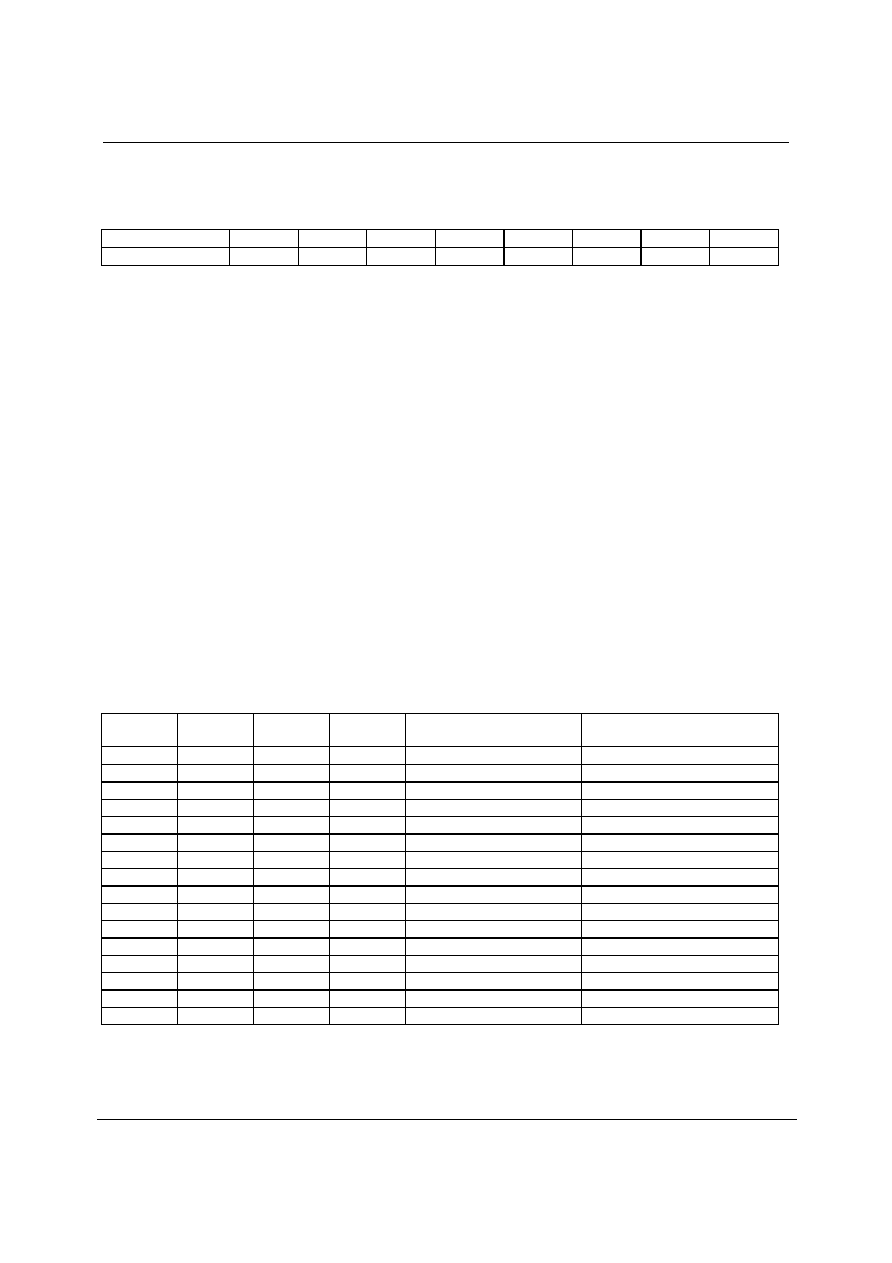
Product Preview
WM8802
w
PP Rev 1.0 May 2003
57
READ REGISTER 2 (GENERAL-PURPOSE I/O INPUT CONTENTS, FS
CALCULATION RESULT, FS COUNTER DATA)
READ REGISTER OUTPUT CONTENTS
REGISTER ADDRESS
DO7
DO6
DO5
DO4
DO3
DO2
DO1
DO0
CCB address: 0xEB
FSC3
FSC2
FSC1
FSC0
GPO3
GPO2
GPO1
GPO0
GPO0
Read data output contents during general-purpose I/O GPO0 input
setting
0: GPIO0 input = Low
1: GPIO0 input = High
GPO1
Read data output contents during general-purpose I/O GPIO1 input
setting
0: GPIO1 input = Low
1: GPIO1 input = High
GPO2
Read data output contents during general-purpose I/O GPIO2 input
setting
0: GPIO2 input = Low
1: GPIO2 input = High
GPO3
Read data output contents during general-purpose I/O GPIO3 input
setting
0: GPIO3 input = Low
1: GPIO3 input = High
FSC [3:0]
Input data fs calculation result
"xxxx": See code table.
FSC3
FSC2
FSC1
FSC0
TARGET FREQUENCY
CALCULATION RANGE(DESIGN
VALUE)
0
0
0
0
Out of range
-
-
-
-
0
0
0
1
-
-
0
0
1
0
-
-
0
0
1
1
-
-
0
1
0
0
16kHz
15.4k to 16.6kHz
0
1
0
1
22.05kHz
21.2k to 22.9kHz
0
1
1
0
24kHz
23.1k to 24.9kHz
0
1
1
1
32kHz
30.8k to 33.3kHz
1
0
0
0
44.1kHz
42.4k to 45.8kHz
1
0
0
1
48kHz
46.2k to 49.9kHz
1
0
1
0
64kHz
615k to 66.7kHz
1
0
1
1
88.2kHz
85.4k to 91.7kHz
1
1
0
0
96kHz
93.1k to 100.7kHz
1
1
0
1
128kHz
122.9k to 1335kHz
1
1
1
0
176.4kHz
170.7k to 180.7kHz
1
1
1
1
192kHz
186.2k to 198.1kHz
Table 21 Input fs Calculation Result Code Table (T
a
= 25�C, AVDD = DVDD = 3.3 V)
WM8802
Product Preview
w
PP Rev 1.0 May 2003
58
READ REGISTER OUTPUT CONTENTS
REGISTER ADDRESS
DO15
DO14
DO13
DO12
DO11
DO10
DO9
DO8
CCB address: 0xEB
FSDAT7
FSDAT6
FSDAT5
FSDAT4
FSDAT3
FSDAT2
FSDAT1
FSDAT0
FSDAT [7:0]
fs counter data output
�
FSDAT [7:0] is the fs calculation counter value. The data length is 8 bits, FSDAT0 is LSB and
FSDAT7 is MSB.
�
The relation between the count value and fs is expressed by the following equation.
fs = 6144/FSDAT (kHz)
�
fs calculation is performed using a 6.144MHz clock so the calculation accuracy is determined
by this clock.
�
The calculation counter value is 8 bit output so the fs that can be calculated is higher than
24kHz.
READ REGISTER 3 (FIRST 48 CHANNEL STATUS BITS)
�
The first 48 channel status bits can be read with the demodulation function.
�
The read channel status data is a LSB output.
�
For read, CCB address is set to 0xEC.
�
The channel status data cannot be updated after the CCB address is set.
�
The relation between the read registers and the channel status data is shown below.
REGISTER
BIT NO.
CONTENTS
REGISTER
BIT NO.
CONTENTS
DO0
Bit 0
Application
DO24
Bit 24
Sampling frequency
DO1
Bit 1
Control
DO25
Bit 25
DO2
Bit 2
DO26
Bit 26
DO3
Bit 3
DO27
Bit 27
DO4
Bit 4
DO28
Bit 28
Clock accuracy
DO5
Bit 5
DO29
Bit 29
DO6
Bit 6
Not defined
DO30
Bit 30
Not defined
DO7
Bit 7
DO31
Bit 31
DO8
Bit 8
Category code
DO32
Bit 32
Word length
DO9
Bit 9
DO33
Bit 33
DO10
Bit 10
DO34
Bit 34
DO11
Bit 11
DO35
Bit 35
DO12
Bit 12
DO36
Bit 36
Not defined
DO13
Bit 13
DO37
Bit 37
DO14
Bit 14
DO38
Bit 38
DO15
Bit 15
DO39
Bit 39
DO16
Bit 16
Source number
DO40
Bit 40
DO17
Bit 17
DO41
Bit 41
DO18
Bit 18
DO42
Bit 42
DO19
Bit 19
DO43
Bit 43
DO20
Bit 20
Channel number
DO44
Bit 44
DO21
Bit 21
DO45
Bit 45
DO22
Bit 22
DO46
Bit 46
DO23
Bit 23
DO47
Bit 47
Product Preview
WM8802
w
PP Rev 1.0 May 2003
59
READ REGISTER 4 (BURST PREAMBLE PC DATA)
The burst preamble Pc data can be read with the demodulation function.
The 16 bits of burst preamble Pc data are output as LSB.
For read, the CCB address is set to OxED.
The relation between the read register and burst preamble Pc data is shown below.
REGISTER
BIT NO.
CONTENTS
DO0
Bit 0
Data type
DO1
Bit 1
DO2
Bit 2
DO3
Bit 3
DO4
Bit 4
DO5
Bit 5
Reserved
DO6
Bit 6
DO7
Bit 7
Error
DO8
Bit 8
Data type dependent
DO9
Bit 9
information
DO10
Bit 10
DO11
Bit 11
DO12
Bit 12
DO13
Bit 13
Bit stream number
DO14
Bit 14
DO15
Bit 15

WM8802
Product Preview
w
PP Rev 1.0 May 2003
60
BURST PREAMBLE PC FIELD
The burst preamble Pc field is shown below.
For the latest information, check the standards issued by each licensee.
REGISTER
VALUE
CONTENTS
DO4 to 0
0
NULL data
1
Dolby AC-3 data
2
Reserved
3
Pause
4
MPEG-1, layer 1 data
5
MPEG-1, layer 2, 3 data, or non-extended MPEG-2
6
Extended MPEG-2 data
7
Reserved
8
MPEG-2, layer 1, low sampling rate
9
MPEG-2, layer 2, 3, low sampling rate
10
Reserved
11
DTS type1
12
DTS type2
13
DTS type3
14
ATRAC
15
ATRACK2/3
16 to 26
Reserved
27
Reserved (MPEG-4, AAC data)
28
MPEG-2, AAC data
29 to 31
Reserved
DO6, 5
0
Reserved (fixed to "0")
DO7
0
Error flag indicating effective burst payload
1
Error flag indicating burst payload error
DO12 to 8
Data type dependent information
DO15 to 13
0
Bit stream No. (fixed to "0")
Table 22 Burst Preamble Pc Field
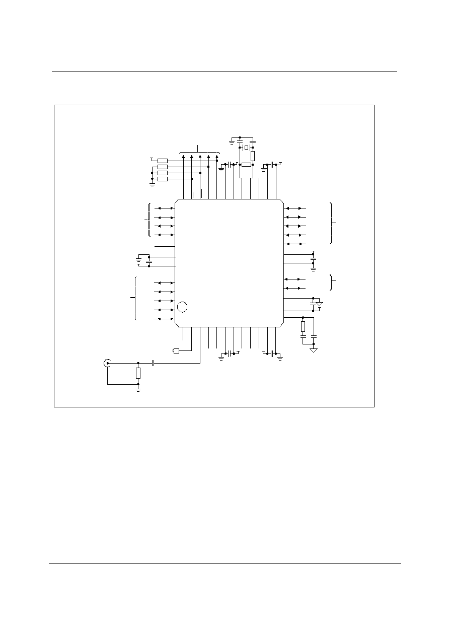
Product Preview
WM8802
w
PP Rev 1.0 May 2003
61
RECOMMENDED EXTERNAL COMPONENTS
21
22
23
24
37
38
39
40
20
35
36
33
34
31
32
29
30
27
28
25
26
WM8802
DO
DI
CE
CL
SLRCK
SDIN
RLRCK
SBCK
RDATA
R
E
R
R
I
N
T
C
K
S
T
E
M
P
H
/
U
O
D
G
N
D
X
I
N
X
O
U
T
X
M
C
K
D
V
D
D
D
G
N
D
DV
D
D
Analogue to Digital
Digital to Analogue
24.576 MHz / 12.288 MHz
Rf
Rp
C
l
C
l
Rd
Rp
Rp
Rp
A
U
D
I
O
/
V
O
Microcontroller
Chip address setting
Chip address setting
Demodulation function
master/slave setting
Modulation/general-purpose
I/O function selection
Cc
Cc
Microcontroller
DVDD
Analogue to Digital
Digital Signal Processing
12
11
10
9
8
7
6
5
4
3
2
1
R
X
0
R
X
3
R
X
1
D
G
N
D
D
V
D
D
D
V
D
D
R
X
6
/
U
I
R
X
O
U
T
R
X
2
R
X
4
R
X
5
/
V
I
D
G
N
D
Cc
Optical Input
Coaxial Input
C
i
R
i
Cc
DVDD DVDD
14
15
13 LPF
AGND
C
0
C
1
R
0
AVDD
Cc
AVDD
17
16 RMCK
RBCK
18
19
DGND
DVDD
Cc
DVDD
44
45
46
47
48
TXO/GPIOEN
TMCK/GPIO0
TBCK/GPIO1
TLRCK/GPIO2
TDATA/GPIO3
42
43
DVDD
DGND
Cc
DVDD
41
XMODE
Figure 34 External Component Diagram
SAMPLEAPPLICATION
A de-coupling capacitor (0.1
�
F) should be connected as close as possible to the power supply pin.
Use a ceramic capacitor with high-frequency characteristics..
A capacitor with a low temperature coefficient should be used for the PLL loop filter.
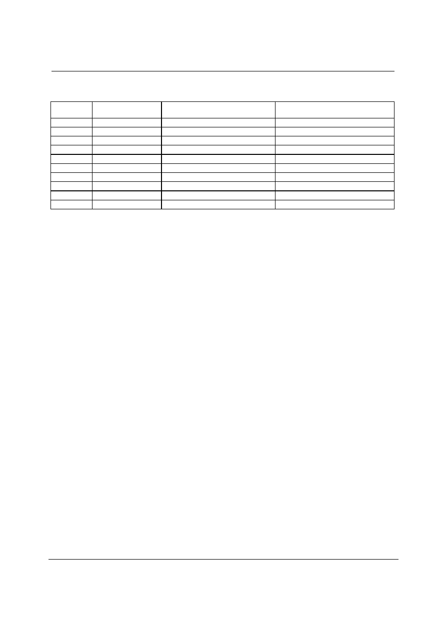
WM8802
Product Preview
w
PP Rev 1.0 May 2003
62
RECOMMENDED EXTERNAL COMPONENTS VALUES
ELEMENT
SYMBOL
RECOMMENDED
CONSTANT
APPLICATION
REMARK
Cc
0.1
�
F
Power supply de-coupling
Ceramic capacitor
Rp
10 k
Function setting pull-down/pull-up
C1
1 pF to 33 pF
Crystal resonator load
NP0 characteristics ceramic capacitor
Rf
1 M
Oscillation amplifier feedback
Rd
220
Oscillation amplifier current limit
Ci
01
�
F
Coaxial input DC cut
Ceramic capacitor
Ri
75
Coaxial input termination
C0
PLL loop filter
Value as required for frequency input range
C1
PLL loop filter
Value as required for frequency input range
R0
PLL loop filter
Value as required for frequency input range
Table 23 Recommended Component Values
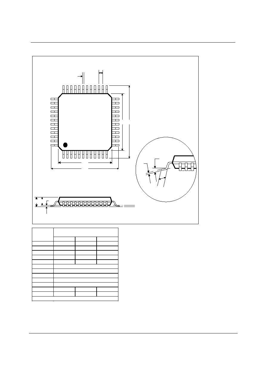
Product Preview
WM8802
w
PP Rev 1.0 May 2003
63
PACKAGEDRAWING
NOTES:
A. ALL LINEAR DIMENSIONS ARE IN MILLIMETERS.
B. THIS DRAWING IS SUBJECT TO CHANGE WITHOUT NOTICE.
C. BODY DIMENSIONS DO NOT INCLUDE MOLD FLASH OR PROTRUSION, NOT TO EXCEED 0.25MM.
DM032.A
FT: 48 PIN SQFP (7 x 7 x 1.0 mm)
Symbols
Dimensions
(mm)
MIN
NOM
MAX
A
-----
-----
1.70
A
1
0.10
A
2
1.50
b
0.18
c
0.15
-----
D
9.00 BSC
D
1
7.00 BSC
E
9.00 BSC
E
1
7.00 BSC
e
0.50 BSC
L
0.50
Tolerances of Form and Position
25
36
e
b
12
1
D1
D
E1
E
13
24
37
48
A A2
A1
c
L
-----
-----
-----
-----
-----
-----
-----
-----
-----
0
o
-----
-----

WM8802
Product Preview
w
PP Rev 1.0 May 2003
64
IMPORTANT NOTICE
Wolfson Microelectronics plc (WM) reserve the right to make changes to their products or to discontinue any product or
service without notice, and advise customers to obtain the latest version of relevant information to verify, before placing
orders, that information being relied on is current. All products are sold subject to the WM terms and conditions of sale
supplied at the time of order acknowledgement, including those pertaining to warranty, patent infringement, and limitation
of liability.
WM warrants performance of its products to the specifications applicable at the time of sale in accordance with WM's
standard warranty. Testing and other quality control techniques are utilised to the extent WM deems necessary to support
this warranty. Specific testing of all parameters of each device is not necessarily performed, except those mandated by
government requirements.
In order to minimise risks associated with customer applications, adequate design and operating safeguards must be used
by the customer to minimise inherent or procedural hazards.
WM assumes no liability for applications assistance or customer product design. WM does not warrant or represent that
any license, either express or implied, is granted under any patent right, copyright, mask work right, or other intellectual
property right of WM covering or relating to any combination, machine, or process in which such products or services might
be or are used. WM's publication of information regarding any third party's products or services does not constitute WM's
approval, license, warranty or endorsement thereof.
Reproduction of information from the WM web site or datasheets is permissible only if reproduction is without alteration and
is accompanied by all associated warranties, conditions, limitations and notices. Representation or reproduction of this
information with alteration voids all warranties provided for an associated WM product or service, is an unfair and deceptive
business practice, and WM is not responsible nor liable for any such use.
Resale of WM's products or services with statements different from or beyond the parameters stated by WM for that
product or service voids all express and any implied warranties for the associated WM product or service, is an unfair and
deceptive business practice, and WM is not responsible nor liable for any such use.
ADDRESS:
Wolfson Microelectronics plc
20 Bernard Terrace
Edinburgh
EH8 9NX
United Kingdom
Tel :: +44 (0)131 272 7000
Fax :: +44 (0)131 272 7001
Email ::
sales@wolfsonmicro.com