Document Outline
- WM8803
- Digital Audio Interface Receiver
- DESCRIPTION
- APPLICATIONS
- BLOCK DIAGRAM
- TABLE OF CONTENTS
- PIN CONFIGURATION
- ORDERING INFORMATION
- PIN DESCRIPTION
- ABSOLUTE MAXIMUM RATINGS
- RECOMMENDED OPERATING CONDITIONS
- ELECTRICAL CHARACTERISTICS
- INPUT AND OUTPUT PIN CAPACITANCE
- DC CHARACTERISTICS
- SYSTEM TIMING REQUIREMENTS
- SERIAL INTERFACE TIMING REQUIREMENTS
- MICRO-CONTROLLER INTERFACE TIMING REQUIREMENTS
- DEVICE DESCRIPTION
- SYSTEM RESET ( PD)
- LOW POWER MODES
- CLOCKS
- DATA INPUT AND OUTPUT
- ERROR OUTPUT AND PROCESSING (ERROR)
- CHANNEL STATUS DATA
- USER GENERAL PURPOSE INTERFACE OUTPUT PORT ( UGPI)
- MICRO-CONTROLLER INTERFACE (E/INT,CE,CL,DI,DO)
- INTERRUPT OUTPUT (E/INT)
- CCB DDRESSES
- DATA WRITE PROCEDURE
- DATA READ PROCEDURE
- I/O TIMING
- WRITE REGISTER TABLE
- WRITE DATA DETAILED DOCUMENTATION
- READ REGISTER TABLE
- READ DATA DETAILED DOCUMENTATION
- SAMPLE APPLICATION
- RECOMMENDED EXTERNAL COMPONENTS
- RECOMMENDED EXTERNAL COMPONENTS V LUES
- PACKAGE DIMENSIONS
WM8803
Digital Audio Interface Receiver
WOLFSON MICROELECTRONICS plc
w :: www.wolfsonmicro.com
Product Preview, September 2003, Rev 1.1
Copyright
2003 Wolfson Microelectronics plc
DESCRIPTION
The WM8803 is a digital audio interface receiver conforming
to IEC 60958/61937 and EIAJ CP-1201. It supports input
audio data rates up to 192kHz and a maximum output data
length of 24 bits.
The WM8803 has a flexible digital output port that allows the
user access to channel status pre-emphasis information, input
signal sampling frequency, sub-code Q data with the
associated CRC flags and other status data.
The WM8803 can output an externally input clock signal that
can be used as an ADC converter clock when the PLL is
unlocked. It also maintains the continuity of the output clock
when the clock is switched.
The WM8803 includes a built-in oscillator and serial data
input circuits and allows the system micro-controller to read
the sub-code Q data and the channel status. It provides
several low-power modes, thus supporting applications that
require long battery life, such as portable audio devices and
PDAs.
The device is available in a 24-pin TSSOP package.
FEATURES
∑
PLL circuit for synchronization with transferred input bi-
phase mark signal.
∑
Input sampling frequency: 32kHz to 192kHz
∑
Outputs clocks: fs, 64fs, and one of 128fs, 256fs, 384fs,
and 512fs.
∑
4-Wire CCB MPU Serial Control or Hardware Default
Interface
∑
Master Clocking Mode
∑
Programmable Audio Data Interface Modes
-
I
2
S, Left, Right Justified
-
16/20/24/32 bit Word Lengths
∑
3.3V Digital supply Operation
∑
5V tolerant digital input ports
APPLICATIONS
∑
DVD Receivers
∑
DVD-R/W Players
∑
Audio Video Receivers
∑
Portable Music Players
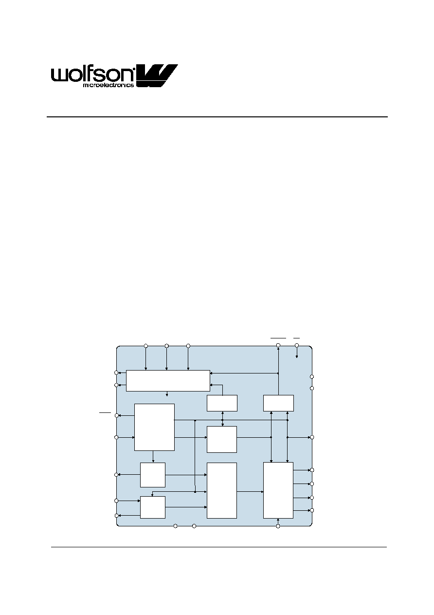
BLOCK DIAGRAM
W
WM8803
PLL
MICROCONTROLLER INTERFACE
DEMODULATION
AND LOCK
DETECTION
DATA
BUFFER
CLOCK
SELECTOR
FS
CALCULATOR
AUDIO
INTERFACE
AMP
C & U
DI
CL
CE
PD
AUDIO
DO
E/INT
UGPI
RXIN
LPF
XIN
XOUT
SDIN
ERROR
CLKOUT
BCLK
LRCLK
SDATO
AVDD
AGND
DVDD
DGND

WM8803
Product Preview
w
PP Rev 1.1 September 2003
2
TABLE OF CONTENTS
DESCRIPTION .......................................................................................................1
FEATURES.............................................................................................................1
APPLICATIONS .....................................................................................................1
BLOCK DIAGRAM .................................................................................................1
TABLE OF CONTENTS .........................................................................................2
PIN CONFIGURATION...........................................................................................3
ORDERING INFORMATION ..................................................................................3
PIN DESCRIPTION ................................................................................................4
ABSOLUTE MAXIMUM RATINGS .........................................................................5
RECOMMENDED OPERATING CONDITIONS .....................................................5
ELECTRICAL CHARACTERISTICS ......................................................................6
INPUT AND OUTPUT PIN CAPACITANCE................................................................... 6
DC CHARACTERISTICS............................................................................................... 6
SYSTEM TIMING REQUIREMENTS ............................................................................. 7
SERIAL INTERFACE TIMING REQUIREMENTS.......................................................... 7
MICRO-CONTROLLER INTERFACE TIMING REQUIREMENTS ................................. 8
DEVICE DESCRIPTION .........................................................................................9
SYSTEM RESET (
_____
PD
)................................................................................................... 9
LOW POWER MODES ................................................................................................. 9
CLOCKS...................................................................................................................... 11
DATA INPUT AND OUTPUT ....................................................................................... 17
ERROR OUTPUT AND PROCESSING (ERROR)....................................................... 22
CHANNEL STATUS DATA .......................................................................................... 24
USER GENERAL PURPOSE INTERFACE OUTPUT PORT (
__________
UGPI
)........................... 24
MICRO-CONTROLLER INTERFACE (E/INT, CE, CL, DI, DO) ...........................28
INTERRUPT OUTPUT (E/INT).................................................................................... 28
CCB ADDRESSES ...................................................................................................... 29
DATA WRITE PROCEDURE....................................................................................... 29
DATA READ PROCEDURE ........................................................................................ 29
I/O TIMING .................................................................................................................. 30
WRITE REGISTER TABLE ......................................................................................... 31
WRITE DATA DETAILED DOCUMENTATION............................................................ 32
READ REGISTER TABLE ........................................................................................... 37
READ DATA DETAILED DOCUMENTATION ............................................................. 38
SAMPLE APPLICATION ......................................................................................41
RECOMMENDED EXTERNAL COMPONENTS ..................................................42
RECOMMENDED EXTERNAL COMPONENTS VALUES ........................................... 43
PACKAGE DIMENSIONS ....................................................................................44
IMPORTANT NOTICE ..........................................................................................45
ADDRESS: .................................................................................................................. 45

Product Preview
WM8803
w
PP Rev 1.1 September 2003
3
PIN CONFIGURATION
ORDERING INFORMATION
DEVICE
TEMP. RANGE
PACKAGE
WM8803SCDT/V
-30 to +70
o
C
24-pin TSSOP
16
15
14
13
5
6
7
1
2
3
4
12
11
8
9
10
17
18
19
20
21
22
23
24
XOUT
ERROR
PD
NC
CE
CL
DI
DO
E/INT
AUDIO
UGPI
RXIN
XIN
SDIN
SDATO
LRCLK
BCLK
CLKOUT
DGND
AGND
NC
LPF
AVDD
DVDD
WM8803
Product Preview
w
PP Rev 1.1 September 2003
4
PIN DESCRIPTION
PIN
NAME
TYPE
DESCRIPTION
1
XOUT
Analogue Output
Oscillation amplifier circuit output pin
2
ERROR
Digital Output
PLL lock error and data error output pin
3
PD
5
Digital Input
System reset and low power mode control input pin (5V tolerant)
4
NC
Digital Input
Non connection
5
CE
5
Digital Input
Micro-controller interface: chip enable input pin (5V tolerant)
6
CL
5
Digital Input
Micro-controller interface: serial clock input pin (5V tolerant)
7
DI
5
Digital Input
Micro-controller interface: write data input pin (5V tolerant)
8
DO
Digital Output
Micro-controller interface: read data output pin
9
E / INT
Digital Output
Pre-emphasis detection or micro-controller interface interrupt output pin
10
AUDIO
Digital Output
Channel status bit 1 non-PCM data detection output pin
11
UGPI
Digital Output
User general purpose interface output pin
1
12
RXIN
5
Digital Input
Digital data input pin (5V tolerant)
13
DVDD
Supply
Digital system power supply
14
AVDD
Supply
Analog system power supply
15
LPF
Analogue Output
PLL loop filter connection pin
16
NC
No connection
17
AGND
Supply
Analog system ground
18
DGND
Supply
Digital system ground
19
CLKOUT
Digital Output
System clock output pin
2
20
BCLK
Digital Output
64fs clock output pin
21
LRCLK
Digital Output
Fs clock output pin
3
22
SDATO
Digital Output
Demodulated data output pin
23
SDIN
Digital Input
Serial digital data input pin (5V tolerant)
24
XIN
Digital Input
Oscillation amplifier element connection or external clock input pin
Notes:
1.
Micro-controller register output or clock switching transition period signal.
2.
128fs, 256fs, 384fs, 512fs, or oscillator amplifier outputs
3.
Other than I
2
S mode;
Low: right channel, High: left channel
I
2
S mode;
Low: left channel, High: right channel
4.
I/O voltage handling: I or O pins: ≠0.3 to +3.6V, except annotated pins: ≠0.3 to +5.5V
5.
To prevent logic circuit latch-up, all power supply levels must be applied or removed simultaneously.

Product Preview
WM8803
w
PP Rev 1.1 September 2003
5
ABSOLUTE MAXIMUM RATINGS
Absolute Maximum Ratings are stress ratings only. Permanent damage to the device may be caused by continuously operating
beyond these limits. Device functional operating limits and guaranteed performance specifications are given under Ele
Characteristics at the test conditions specified.
ESD Sensitive Device. This device is manufactured on a CMOS process. It is therefore generically suscept
damage from excessive static voltages. Proper ESD precautions must be taken during handling and storage
device.
CONDITION
SYMBOL
CONDITIONS
MIN - MAX
Maximum supply voltage
AVDD
max
1
≠0.3 to 4.6V
Maximum supply voltage
DVDD
max
2
≠0.3 to 4.6V
Input voltage 1
V
IN1
3
≠0.3 to VDD + 0.3V
Input voltage 2
V
IN2
4
≠0.3 to 5.8V
Storage temperature
T
stg
≠55 to 125∞C
Operating temperature
T
opg
≠30 to 70∞C
Maximum output current
I
i
, I
o
5
±20 mA
Notes:
1.
AVDD pin
2.
DVDD pin
3.
XIN pin
4.
RXIN, SDIN, PD, CE, CL, and DI pins
5.
Per single input or output pin
RECOMMENDED OPERATING CONDITIONS
PARAMETER
SYMBOL
TEST CONDITIONS
MIN
TYP
MAX
UNIT
Supply voltage 1
AVDD, DVDD
1
2.7
3.3
3.6
V
Supply voltage 2
AVDD, DVDD
2
3.0
3.3
3.6
V
Input voltage range 1
V
IN1
3
0
3.3
3.6
V
Input voltage range 2
V
IN2
4
0
3.3
5.5
V
Operating temperature
T
opg
≠30
--
70
∞C
Notes:
1.
PLLCK [1:0] = "00" or PLLCK [1:0] = "01"
2.
PLLCK [1:0] = "10" or PLLCK [1:0] = "11"
3.
XIN pin
4.
RXIN, SDIN, PD , CE, CL, and DI pins