 | –≠–ª–µ–∫—Ç—Ä–æ–Ω–Ω—ã–π –∫–æ–º–ø–æ–Ω–µ–Ω—Ç: WM8951 | –°–∫–∞—á–∞—Ç—å:  PDF PDF  ZIP ZIP |
Document Outline
- WM8951L
- Stereo ADC with Microphone Input and Clock Generator
- DESCRIPTION
- FEATURES
- APPLICATIONS
- BLOCK DIAGRAM
- TABLE OF CONTENTS
- PIN CONFIGURATION
- ORDERING INFORMATION
- PIN DESCRIPTION
- ABSOLUTE MAXIMUM RATINGS
- RECOMMENDED OPERATING CONDITIONS
- ELECTRICAL CHARACTERISTICS
- POWER CONSUMPTION
- MASTER CLOCK TIMING
- DIGITAL AUDIO INTERFACE Ö MASTER MODE
- DIGITAL AUDIO INTERFACE Ö SLAVE MODE
- MPU INTERFACE TIMING
- DEVICE DESCRIPTION
- INTRODUCTION
- AUDIO SIGNAL PATH
- DEVICE OPERATION
- AUDIO DATA SAMPLING RATES
- ACTIVATING DSP AND DIGITAL AUDIO INTERFACE
- SOFTWARE CONTROL INTERFACE
- POWER DOWN MODES
- REGISTER MAP
- DIGITAL FILTER CHARACTERISTICS
- TERMINOLOGY
- ADC FILTER RESPONSES
- ADC HIGH PASS FILTER
- APPLICATIONS INFORMATION
- RECOMMENDED EXTERNAL COMPONENTS
- PACKAGE DIMENSIONS
- IMPORTANT NOTICE
- ADDRESS:
w
WM8951L
Stereo ADC with Microphone Input and Clock Generator
WOLFSON MICROELECTRONICS plc
To receive regular email updates, sign up
at
http://www.wolfsonmicro.com/enews/
Production Data, May 2005, Rev 4.0
Copyright
2005 Wolfson Microelectronics plc
DESCRIPTION
The WM8951L is a low power stereo ADC with an
integrated microphone interface and crystal oscillator for
clock generation. The WM8951L is ideal for voice recorders,
wireless microphones and games console accessories.
Stereo line and mono microphone level audio inputs are
provided, along with a mute function, programmable line
level volume control and a bias voltage output suitable for
an electret type microphone.
Stereo 24-bit multi-bit sigma delta ADCs are used with
oversampling decimation filters. Digital audio input word
lengths from 16-32 bits and sampling rates from 8kHz to
96kHz are supported.
The device is controlled via a 2 or 3 wire serial interface.
The interface provides access to all features including
volume controls, mutes and extensive power management
facilities. The device is available in a small 28 lead 5x5mm
quad flat leadless package (QFN).
FEATURES
∑ Audio Performance
-
ADC SNR 90dB (`A' weighted) at 3.3V, 85dB at 1.8V
-
Low Power
-
1.42 ≠ 3.6V Digital Supply Operation
-
1.8 ≠ 3.6V Analogue Supply Operation
∑ Sampling Frequency: 8kHz ≠ 96kHz
∑ Selectable ADC High Pass Filter
∑ 2 or 3-Wire MPU Serial Control Interface
∑ Programmable Audio Data Interface Modes
-
I
2
S, Left, Right Justified or DSP
-
16/20/24/32 bit Word Lengths
-
Master or Slave Clocking Mode
∑ Microphone Input and Electret Bias with Side Tone Mixer
∑ Available in 5x5mm 28-pin QFN package
APPLICATIONS
∑ Wireless microphones
∑ Voice recorders
∑ Games console accessories
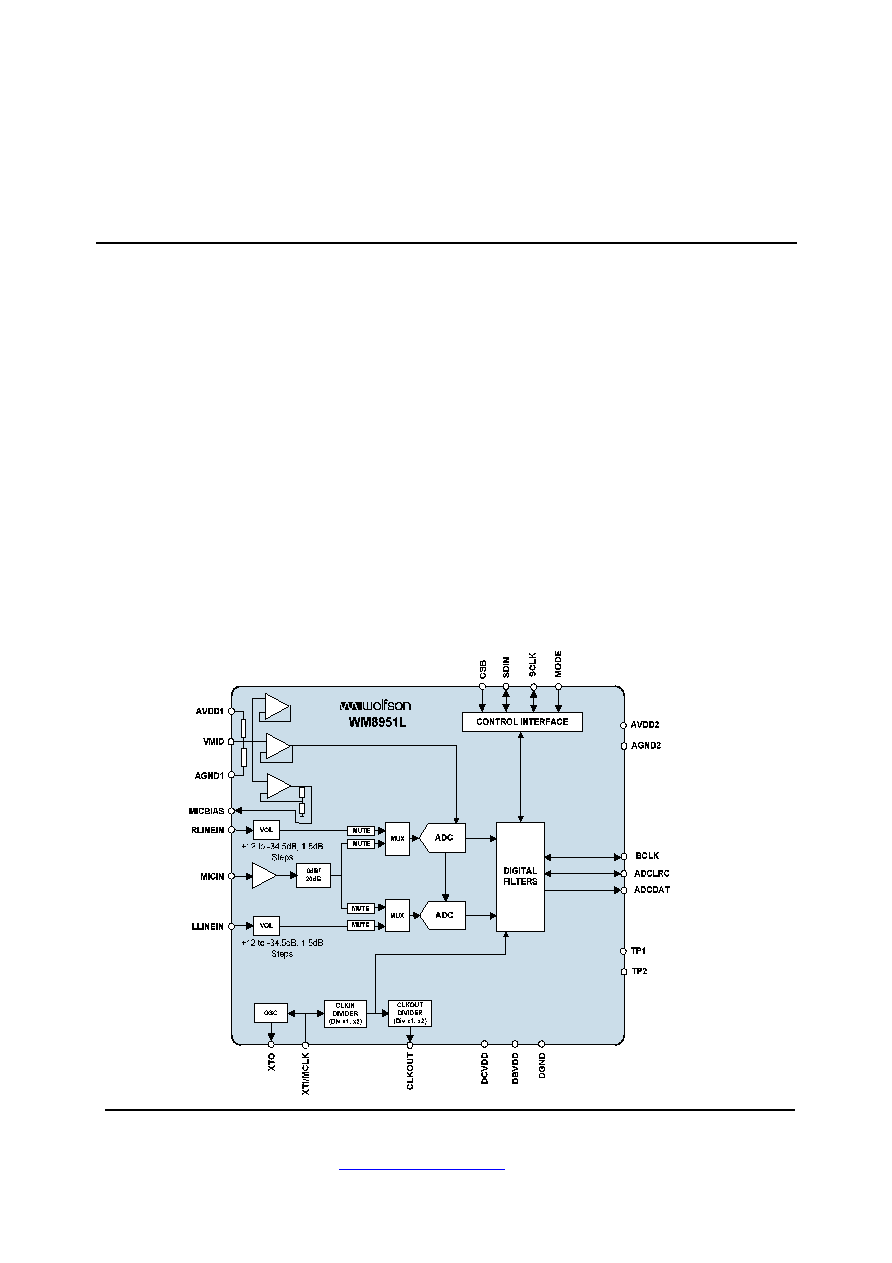
BLOCK DIAGRAM

WM8951L
Production Data
w
PD Rev 4.0 May 2005
2
TABLE OF CONTENTS
DESCRIPTION.......................................................................................................1
FEATURES.............................................................................................................1
APPLICATIONS .....................................................................................................1
BLOCK DIAGRAM .................................................................................................1
PIN CONFIGURATION...........................................................................................3
ORDERING INFORMATION ..................................................................................3
PIN DESCRIPTION ................................................................................................4
ABSOLUTE MAXIMUM RATINGS .........................................................................5
RECOMMENDED OPERATING CONDITIONS .....................................................5
ELECTRICAL CHARACTERISTICS ......................................................................6
TERMINOLOGY .....................................................................................................7
POWER CONSUMPTION ......................................................................................8
MASTER CLOCK TIMING......................................................................................9
DIGITAL AUDIO INTERFACE ≠ MASTER MODE ....................................................... 10
DIGITAL AUDIO INTERFACE ≠ SLAVE MODE .......................................................... 11
MPU INTERFACE TIMING .......................................................................................... 12
DEVICE DESCRIPTION.......................................................................................14
INTRODUCTION ......................................................................................................... 14
AUDIO SIGNAL PATH................................................................................................. 14
DEVICE OPERATION ................................................................................................. 20
AUDIO DATA SAMPLING RATES............................................................................... 25
ACTIVATING DSP AND DIGITAL AUDIO INTERFACE .............................................. 30
SOFTWARE CONTROL INTERFACE......................................................................... 30
POWER DOWN MODES ............................................................................................ 32
REGISTER MAP ......................................................................................................... 34
DIGITAL FILTER CHARACTERISTICS ...............................................................37
TERMINOLOGY .......................................................................................................... 37
ADC FILTER RESPONSES .................................................................................38
ADC HIGH PASS FILTER ........................................................................................... 39
APPLICATIONS INFORMATION .........................................................................40
RECOMMENDED EXTERNAL COMPONENTS .......................................................... 40
PACKAGE DIMENSIONS ....................................................................................41
IMPORTANT NOTICE ..........................................................................................42
ADDRESS: .................................................................................................................. 42

Production Data
WM8951
w
PD Rev 4.0 May 2005
3
PIN CONFIGURATION
ORDERING INFORMATION
DEVICE
TEMPERATURE
RANGE
AVDD
RANGE
PACKAGE
MOISTURE
SENSITIVITY LEVEL
PEAK SOLDERING
TEMPERATURE
WM8951LGEFL
-25 to +85
o
C
1.8 to 3.6V
28 pin QFN
(lead free)
MSL 1
260∞C
WM8951LGEFL/R
-25 to +85
o
C
1.8 to 3.6V
28 pin QFN
(lead free, tape and
reel)
MSL 1
260∞C
Note:
Reel quantity = 3,500

WM8951L
Production Data
w
PD Rev 4.0 May 2005
4
PIN DESCRIPTION
PIN
NAME
TYPE
DESCRIPTION
1
XTI/MCLK
Digital Input
Crystal Input or Master Clock Input (MCLK)
2
XTO
Digital Output
Crystal Output
3
DCVDD
Supply
Digital Core VDD
4
DGND
Ground
Digital GND
5
DBVDD
Supply
Digital Buffers VDD
6
CLKOUT
Digital Output
Buffered Clock Output
7
BCLK
Digital Input/Output
Digital Audio Bit Clock, Pull Down, (see Note 1)
8
TP1
Test Pin
Connect to ground
9
TP2
Test Pin
Connect to ground in slave mode / Leave floating in master
mode
10
ADCDAT
Digital Output
ADC Digital Audio Data Output
11
ADCLRC
Digital Input/Output
ADC Sample Rate Left/Right Clock, Pull Down (see Note 1)
12
AVDD2
Supply
Analogue VDD
13
DNC
Do Not Connect
Leave this pin floating
14
DNC
Do Not Connect
Leave this pin floating
15
AGND2
Ground
Analogue GND
16
DNC
Do Not Connect
Leave this pin floating
17
DNC
Do Not Connect
Leave this pin floating
18
AVDD
Supply
Analogue VDD
19
AGND
Ground
Analogue GND
20
VMID
Analogue Output
Mid-rail reference decoupling point
21
MICBIAS
Analogue Output
Electret Microphone Bias
22
MICIN
Analogue Input
Microphone Input (AC coupled)
23
RLINEIN
Analogue Input
Right Channel Line Input (AC coupled)
24
LLINEIN
Analogue Input
Left Channel Line Input (AC coupled)
25
MODE
Digital Input
Control Interface Selection, Pull Up (see Note 1)
26
CSB
Digital Input
3-Wire MPU Chip Select/ 2-Wire MPU interface address
selection, active low, Pull up (see Note 1)
27
SDIN
Digital Input/Output
3-Wire MPU Data Input / 2-Wire MPU Data Input
28
SCLK
Digital Input
3-Wire MPU Clock Input / 2-Wire MPU Clock Input
Note:
1.
Pull Up/Down only present when Control Register Interface ACTIVE=0 to conserve power.
2.
It is recommended that the QFN ground paddle should be connected to analogue ground on the application PCB.

Production Data
WM8951
w
PD Rev 4.0 May 2005
5
ABSOLUTE MAXIMUM RATINGS
Absolute Maximum Ratings are stress ratings only. Permanent damage to the device may be caused by continuously operating at
or beyond these limits. Device functional operating limits and guaranteed performance specifications are given under Electrical
Characteristics at the test conditions specified.
ESD Sensitive Device. This device is manufactured on a CMOS process. It is therefore generically susceptible
to damage from excessive static voltages. Proper ESD precautions must be taken during handling and storage
of this device.
Wolfson tests its package types according to IPC/JEDEC J-STD-020B for Moisture Sensitivity to determine acceptable storage
conditions prior to surface mount assembly. These levels are:
MSL1 = unlimited floor life at <30
∞C / 85% Relative Humidity. Not normally stored in moisture barrier bag.
MSL2 = out of bag storage for 1 year at <30
∞C / 60% Relative Humidity. Supplied in moisture barrier bag.
MSL3 = out of bag storage for 168 hours at <30
∞C / 60% Relative Humidity. Supplied in moisture barrier bag.
The Moisture Sensitivity Level for each package type is specified in Ordering Information.
CONDITION
MIN
MAX
Digital supply voltage
-0.3V
+3.63V
Analogue supply voltage
-0.3V
+3.63V
Voltage range digital inputs
DGND -0.3V
DVDD +0.3V
Voltage range analogue inputs
AGND1/2 -0.3V
AVDD1/2 +0.3V
Operating temperature range, T
A
-25
∞C
+85
∞C
Notes:
1.
Analogue and digital grounds must always be within 0.3V of each other.
2.
The digital supply core voltage (DCVDD) must always be less than or equal to the analogue supply voltage
(AVDD1/2)
RECOMMENDED OPERATING CONDITIONS
PARAMETER
SYMBOL
TEST
CONDITIONS
MIN
TYP
MAX
UNIT
Digital supply range (Core)
DCVDD
1.42
1.5
3.6
V
Digital supply range (Buffer)
DBVDD
1.8
3.6
V
Analogue supply range
AVDD1, AVDD2
1.8
3.6
V
Ground
DGND, AGND1, AGND2
0
V