WM8955L
STEREO DAC FOR PORTABLE AUDIO APPLICATIONS
WOLFSON MICROELECTRONICS PLC
www.wolfsonmicro.com
Product Preview, May2003, Rev 0.4
Copyright
2003 Wolfson Microelectronics plc
DESCRIPTION
The WM8955L is a low power, high qualitystereo DAC with
integrated headphone and loudspeaker amplifiers, designed
to reduce external component requirements in portable digital
audio applications.
The on-chip headphone amplifiers can deliver 40mW into a
16
load. Advanced on-chip digital signal processing
performs bass and treble tone control.
The WM8955L can operate as a master or a slave, and
includes an on-chip PLL. It can use most master clock
frequencies commonlyfound in portable sy
stems, including
USB, GSM, CDMA or PDC clocks, or standard 256f
s
clock
rates. Different audio sample rates such as 48kHz, 44.1kHz,
8kHz and manyothers are supported.
The WM8955L operates on supplyvoltages from 1.8V up to
3.6V, although the digital core can operate on a separate
supplydown to 1.42V, saving power. Different sections of the
chip can also be powered down under software control.
The WM8955L is supplied in a verysmall and thin 5x5mm
QFN package, ideal for use in hand-held and portable
systems.
FEATURES
�
DAC SNR 98dB, THD -95dB (`A' weighted @ 48kHz, 3.3V)
�
On-chip 400mW BTL Speaker Driver (mono)
�
On-chip Headphone Driver
�
40mW output power on 16
/ 3.3V
�
THD �80dB at 20mW, SNR 90dB with 16
load
�
Stereo and Mono Line-in mix into DAC output
�
SeparatelyMixed Stereo and Mono Outputs
�
Digital Tone Control and Bass Boost
�
Low Power
�
Down to 7mW for stereo playback (1.8V / 1.5V supplies)
�
10
�
W StandbyMode
�
Low SupplyVoltages
�
Analogue 1.8V to 3.6V
�
Digital core: 1.42V to 3.6V
�
Digital I/O: 1.42V to 3.6V
�
Master clocks supported: GSM, CDMA, PDC, USB or
standard audio clocks
�
Audio sample rates supported: 8, 11.025, 12, 16, 22.05, 24,
32, 44.1, 48, 88.2, 96kHz
�
32-pin QFN package, 5x5x0.9mm size, 0.5mm lead pitch
APPLICATIONS
�
Smartphone / Multimedia Phone
�
Digital Audio Player
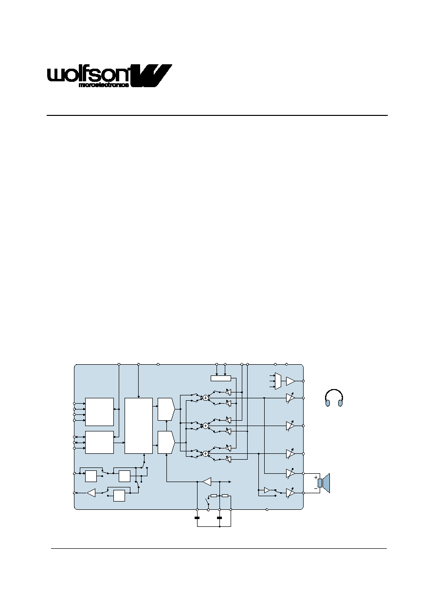
BLOCK DIAGRAM
DAC
LI2LO
MI2LO
MI2RO
RI2RO
LI2MO
RI2MO
LD2LO
RD2LO
LD2MO
RD2MO
LD2RO
RD2RO
LEFT
MIXER
RIGHT
MIXER
MONO
MIXER
HPDETECT
DCVDD
DBVDD
DGND
DIGITAL
FILTERS
TONE
CONTROL
DIGITAL
AUDIO
INTERFACE
BCLK
DACDAT
DACLRC
VR
EF
AV
D
D
AG
N
D
VM
I
D
50K
50K
W
WM8955L
VR
E
F
LI
N
E
I
N
L
LI
N
E
I
N
R
DAC
CONTROL
INTERFACE
CSB
SDIN
SCLK
MODE
ROUT1VOL
LOUT1VOL
MONOVOL
LOUT1
ROUT1
MONOOUT
LOUT2
ROUT2
-1
H
PVD
D
HP
G
N
D
ROUT2
INV
Loudspeaker
L - (-R)
= L+R
ROUT2VOL
LOUT2VOL
OUT3
VREF
MONOOUT
M
U
X
ROUT1
VREF
-1
MO
NO
I
N
+
MO
NO
I
N
-
DIFF. IN
MCLK
f/2
PLL
CLKOUT
f/2
MCLK
SEL
CLKOUT
SEL
MCLK
DIV2
CLKOUT
DIV2
WM8955L
Product Preview
w
Product Preview Rev 0.4 May2003
2
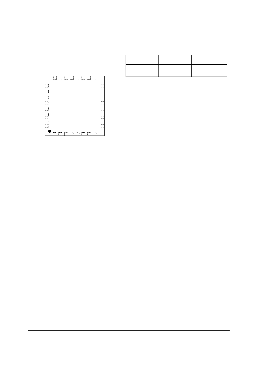
PIN CONFIGURATION
ORDERING INFORMATION
ORDER CODE
TEMPERATURE
RANGE
PACKAGE
WM8955LEFL
-25
�
C to +85
�
C
32-pin QFN
(5x5x0.9mm)
1
2
3
4
5
6
7
8
24
23
22
21
20
19
18
17
16
15
14
13
12
11
10
9
25
26
27
28
29
30
31
32
DACDAT
BC
LK
DC
V
D
D
DGND
DBVDD
MCL
K
DA
CL
RC
OUT3
AV
D
D
VM
I
D
AG
N
D
VR
E
F
NC
HPDETECT
HPGND
PLLGND
MONOOUT
HPVDD
ROUT1
LOUT1
ROUT2
LOUT2
CL
KO
UT
CSB
MODE
MONOIN+
LINEINL
LINEINR
MONOIN-
SDIN
SCLK
NC
Product Preview
WM8955L
w
Product Preview Rev 0.4 May2003
3
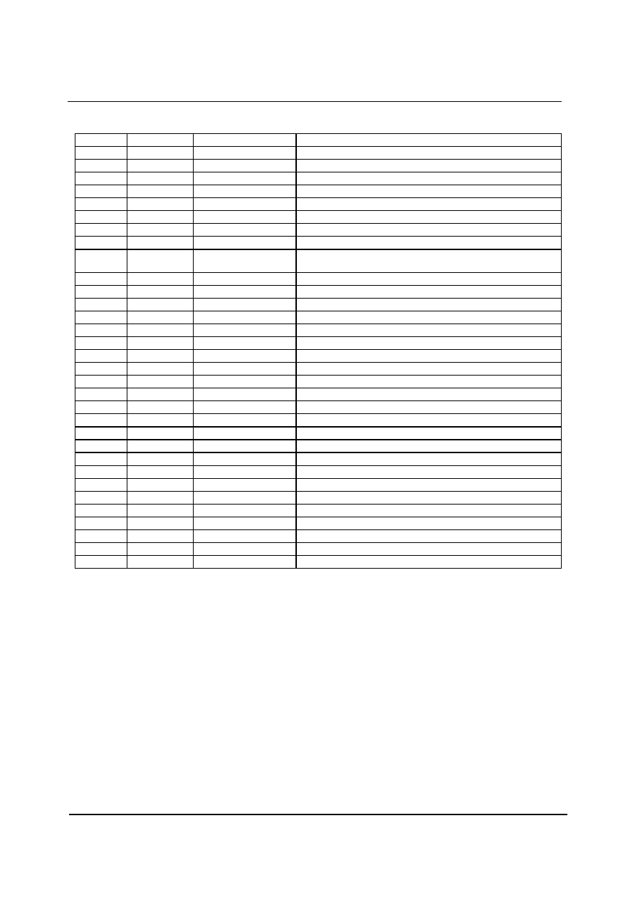
PIN DESCRIPTION
PIN #
NAME
TYPE
DESCRIPTION
1
MCLK
Digital Input
Master Clock
2
DCVDD
SupplyDigital Core Supply
3
DBVDD
SupplyDigital Buffer (I/O) Supply
4
DGND
SupplyDigital Ground (return path for both DCVDD and DBVDD)
5
BCLK
Digital Input / Output
Audio Interface Bit Clock
6
DACDAT
Digital Input
DAC Digital Audio Data
7
DACLRC
Digital Input / Output
Audio Interface Left / Right Clock
8
CLKOUT
Digital Output
Buffered Clock Output (from MCLK or internal PLL)
9
PLLGND
SupplyInternally
connected to AGND. Connect this pin to AGND externally
for best PLL performance, or leave floating.
10
MONOOUT
Analogue Output
Mono Output
11
OUT3
Analogue Output
Output 3 (can be used as Headphone Pseudo Ground)
12
ROUT1
Analogue Output
Right Output 1 (Line or Headphone)
13
LOUT1
Analogue Output
Left Output 1 (Line or Headphone)
14
HPGND
SupplySupply
for Analogue Output Drivers (LOUT1/2, ROUT1/2)
15
ROUT2
Analogue Output
Right Output 1 (Line or Headphone or Speaker)
16
LOUT2
Analogue Output
Left Output 1 (Line or Headphone or Speaker)
17
HPVDD
SupplySupply
for Analogue Output Drivers (LOUT1/2, ROUT1/2, MONOUT)
18
AVDD
SupplyAnalogue Supply
19
AGND
SupplyAnalogue Ground (return path for AVDD)
20
VREF
Analogue Output
Reference Voltage Decoupling Capacitor
21
VMID
Analogue Output
Midrail Voltage Decoupling Capacitor
22
NC
No Connect
No Internal Connection
23
HPDETECT
Logic Input
Headphone / Speaker switch (referred to AVDD)
24
NC
No Connect
No Internal Connection
25
MONOIN-
Analogue Input
Negative end of MONOIN+, for differential mono signals
26
MONOIN+
Analogue Input
Analogue Line-in to mixers (mono channel)
27
LINEINR
Analogue Input
Analogue Line-in to mixers (right channel)
28
LINEINL
Analogue Input
Analogue Line-in to mixers (left channel)
29
MODE
Digital Input
Control Interface Selection
30
CSB
Digital Input
Chip Select / Device Address Selection
31
SDIN
Digital Input/Output
Control Interface Data Input / 2-wire Acknowledge output
32
SCLK
Digital Input
Control Interface Clock Input
WM8955L
Product Preview
w
Product Preview Rev 0.4 May2003
4
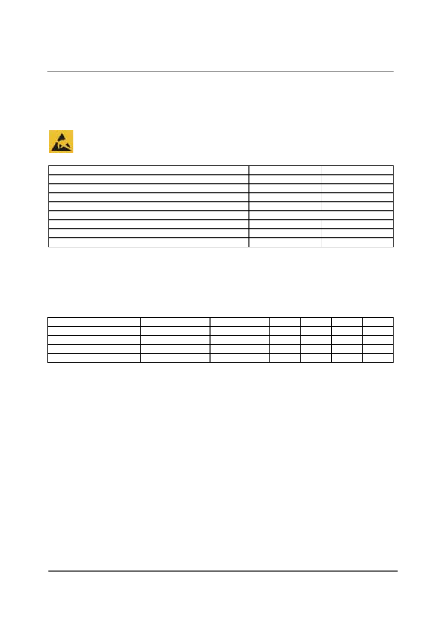
ABSOLUTE MAXIMUM RATINGS
Absolute Maximum Ratings are stress ratings only. Permanent damage to the device maybe caused bycontinuously
operating at or beyond these limits. Device functional operating limits and guaranteed performance specifications are given
under Electrical Characteristics at the test conditions specified.
ESD Sensitive Device. This device is manufactured on a CMOS process. It is therefore genericallysusceptible
to damage from excessive static voltages. Proper ESD precautions must be taken during handling and storage
of this device.
CONDITION
MIN
MAX
Supplyvoltages
-0.3V
+3.63V
Voltage range digital inputs
DGND -0.3V
DBVDD +0.3V
Voltage range analogue inputs
AGND -0.3V
AVDD +0.3V
Operating temperature range, T
A
-25
�
C
+85
�
C
Storage temperature prior to soldering
30
�
C max / 85% RH max
Storage temperature after soldering
-65
�
C
+150
�
C
Package bodytemperature (soldering 10 seconds)
+260
�
C
Package bodytemperature (soldering 2 minutes)
+183
�
C
Notes
1.
Analogue and digital grounds must always be within 0.3V of each other.
2.
All digital and analogue supplies are completelyindependent from each other.
RECOMMENDED OPERATING CONDITIONS
PARAMETER
SYMBOL
TEST CONDITIONS
MIN
TYP
MAX
UNIT
Digital supplyrange (Core)
DCVDD
1.42
2.0
3.6
V
Digital supplyrange (Buffer)
DBVDD
1.8
2.0
3.6
V
Analogue supplies range
AVDD, HPVDD
1.8
2.0
3.6
V
Ground
DGND, AGND, HPGND
0
V
Product Preview
WM8955L
w
Product Preview Rev 0.4 May2003
5
ELECTRICAL CHARACTERISTICS
Test Conditions
DCVDD = 1.5V, AVDD = HPVDD = 3.3V, T
A
= +25
o
C, 1kHz signal, fs = 48kHz, 24-bit audio data unless otherwise stated.
PARAMETER
SYMBOL
TEST CONDITIONS
MIN
TYP
MAX
UNIT
DAC to Line-Out (LOUT1/2, ROUT1/2, MONOOUT with 10k
/ 50pF load)
AVDD = 3.3V
98
Signal to Noise Ratio
(A-weighted)
SNR
AVDD = 1.8V
95
dB
AVDD = 3.3V
-95
Total Harmonic Distortion
THD
AVDD = 1.8V
-90
dB
Channel Separation
1kHz signal
90
dB
Analogue Mixer Inputs (LINEINL, LINEINR, MONOIN)
AVDD = 3.3V
1.0
Full-scale Input Signal Level
V
INFS
AVDD = 1.8V
0.516
V rms
AVDD = 3.3V
95
Signal to Noise Ratio
Line-in to Line-Out
(A-weighted)
SNR
AVDD = 1.8V
90
dB
AVDD = 3.3V
-92
dB
Total Harmonic Distortion
THD
AVDD = 1.8V
-92
dB
PGA gain = 0dB
20
Input Resistance
(signal enters one mixer only)
PGA gain = +6dB
10
PGA gain = 0dB
10
Input Resistance
(signal enters two mixers)
R
LINEIN
PGA gain = +6dB
5
k
MONOIN- input resistance
R
MONOIN-
anygain
20
k
Programmable Gain
-15
+6
dB
Programmable Gain Step Size
Monotonic
3
dB
Mute Attenuation
TBD
dB
Analogue Outputs (LOUT1/2, ROUT1/2, MONOOUT)
0dB Full scale output voltage
AVDD/3.3
Vrms
Programmable Gain
1kHz signal
-67
+6
dB
Programmable Gain Steps
Monotonic
80
steps
Mute attenuation
1kHz, full scale signal
85
dB
Channel Separation
80
90
dB
Headphone Output (LOUT1/2, ROUT1/2 with 16 or 32 Ohm load)
Output Power per channel
P
O
Output power is verycloselycorrelated with THD; see below.
HPVDD=1.8V, R
L
=32
P
O
=5mW
0.013
-78
HPVDD=1.8V, R
L
=16
P
O
=5mW
0.013
-78
HPVDD=3.3V, R
L
=32
,
P
O
=20mW
0.01
-80
Total Harmonic Distortion
THD
HPVDD=3.3V, R
L
=16
,
P
O
=20mW
0.01
-80
%
dB
HPVDD = 3.3V
90
dB
Signal to Noise Ratio
(A-weighted)
SNR
HPVDD = 1.8V
90
dB