 | –≠–ª–µ–∫—Ç—Ä–æ–Ω–Ω—ã–π –∫–æ–º–ø–æ–Ω–µ–Ω—Ç: WM8976 | –°–∫–∞—á–∞—Ç—å:  PDF PDF  ZIP ZIP |
Document Outline
- WM8976
- Low Power CODEC With Speaker Driver
- DESCRIPTION
- FEATURES
- APPLICATIONS
- TABLE OF CONTENTS
- PIN CONFIGURATION
- ORDERING INFORMATION
- PIN DESCRIPTION
- ABSOLUTE MAXIMUM RATINGS
- RECOMMENDED OPERATING CONDITIONS
- ELECTRICAL CHARACTERISTICS
- SPEAKER OUTPUT THD VERSUS POWER
- POWER CONSUMPTION
- SIGNAL TIMING REQUIREMENTS
- SYSTEM CLOCK TIMING
- AUDIO INTERFACE TIMING Ö MASTER MODE
- AUDIO INTERFACE TIMING Ö SLAVE MODE
- CONTROL INTERFACE TIMING Ö 3-WIRE MODE
- CONTROL INTERFACE TIMING Ö 2-WIRE MODE
- INTERNAL POWER ON RESET CIRCUIT
- RECOMMENDED POWER UP/DOWN SEQUENCE
- DEVICE DESCRIPTION
- INTRODUCTION
- INPUT SIGNAL PATH
- ANALOGUE TO DIGITAL CONVERTER (ADC)
- INPUT LIMITER / AUTOMATIC LEVEL CONTROL (ALC)
- OUTPUT SIGNAL PATH
- OUTPUT SIGNAL PATH
- 3D STEREO ENHANCEMENT
- ANALOGUE OUTPUTS
- DIGITAL AUDIO INTERFACES
- AUDIO SAMPLE RATES
- MASTER CLOCK AND PHASE LOCKED LOOP (PLL)
- GENERAL PURPOSE INPUT/OUTPUT
- OUTPUT SWITCHING (JACK DETECT)
- CONTROL INTERFACE
- RESETTING THE CHIP
- POWER SUPPLIES
- POWER MANAGEMENT
- REGISTER MAP
- DIGITAL FILTER CHARACTERISTICS
- TERMINOLOGY
- DAC FILTER RESPONSES
- ADC FILTER RESPONSES
- HIGHPASS FILTER
- 5-BAND EQUALISER
- APPLICATIONS INFORMATION
- RECOMMENDED EXTERNAL COMPONENTS
- PACKAGE DIAGRAM
- IMPORTANT NOTICE
w
WM8976
Low Power CODEC With Speaker Driver
WOLFSON MICROELECTRONICS plc
www.wolfsonmicro.com
Preliminary Technical Data, February 2005, Rev 2.0
Copyright
2005 Wolfson Microelectronics plc
.
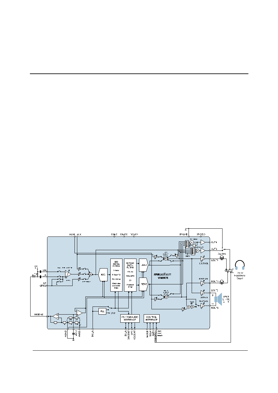
DESCRIPTION
The WM8976 is a low power, high quality codec designed for
portable applications such as Digital still camera or Digital
Camcorder.
The device integrates a preamp for a differential mic, and
includes drivers for speakers, headphone and differential or
stereo line output. External component requirements are
reduced as no separate microphone or headphone amplifiers
are required.
Advanced on-chip digital signal processing includes a 5-band
equaliser, a mixed signal Automatic Level Control for the
microphone or line input through the ADC as well as a purely
digital limiter function for record or playback. Additional digital
filtering options are available in the ADC path, to cater for
application filtering such as `wind noise reduction'.
The WM8976 CODEC can operate as a master or a slave. An
internal PLL can generate all required audio clocks for the
Codec from common reference clock frequencies, such as
12MHz and 13MHz.
The WM8976 operates at analogue supply voltages from 2.5V
to 3.6V, although the digital core can operate at voltages down
to 1.8V to save power. The speaker outputs and OUT3/4 line
outputs can run from a 5V supply if increased output power is
required. Individual sections of the chip can also be powered
down under software control.
FEATURES
∑ Stereo Codec:
∑ DAC SNR 98dB, THD -84dB (`A' weighted @ 48kHz)
∑ ADC SNR 90dB, THD -80dB (`A' weighted @ 48kHz)
∑ On-chip Headphone Driver with `capless' option
-
40mW output power into 16
/ 3.3V SPKVDD
∑ 0.9W output power into 8 BTL speaker / 5V SPKVDD
-
Capable of driving piezo speakers
-
Stereo speaker drive configuration
∑ Mic Preamps:
∑ Differential or single-ended microphone Interface
-
Programmable preamp gain
-
Psuedo differential input with common mode rejection
-
Programmable ALC / Noise Gate in ADC path
∑ Low-noise bias supplied for electret microphones
∑ Other features:
∑ Enhanced 3-D function for improved stereo separation
∑ Digital playback limiter
∑ 5-band Equaliser (record or playback)
∑ Programmable ADC High Pass Filter (wind noise reduction)
∑ Programmable ADC Notch Filter
∑ Aux inputs for stereo analog input signals or `beep'
∑ On-chip PLL supporting 12, 13, 19.2MHz and other clocks
∑ Low power, low voltage
-
2.5V to 3.6V (digital core: 1.8V to 3.6V)
-
power consumption <30mW all-on with 2.5V supplies
∑ 5x5mm 32-pin QFN package
APPLICATIONS
∑ Stereo Camcorder or DSC

WM8976
Preliminary Technical Data
w
PTD Rev 2.0 February 2005
2
TABLE OF CONTENTS
DESCRIPTION .......................................................................................................1
FEATURES.............................................................................................................1
APPLICATIONS .....................................................................................................1
PIN CONFIGURATION...........................................................................................3
ORDERING INFORMATION ..................................................................................3
PIN DESCRIPTION ................................................................................................4
ABSOLUTE MAXIMUM RATINGS .........................................................................5
RECOMMENDED OPERATING CONDITIONS .....................................................5
ELECTRICAL CHARACTERISTICS ......................................................................6
TERMINOLOGY............................................................................................................ 8
SPEAKER OUTPUT THD VERSUS POWER ......................................................10
POWER CONSUMPTION ....................................................................................11
SIGNAL TIMING REQUIREMENTS .....................................................................12
SYSTEM CLOCK TIMING ........................................................................................... 12
AUDIO INTERFACE TIMING ≠ MASTER MODE ........................................................ 12
AUDIO INTERFACE TIMING ≠ SLAVE MODE............................................................ 13
CONTROL INTERFACE TIMING ≠ 3-WIRE MODE .................................................... 14
CONTROL INTERFACE TIMING ≠ 2-WIRE MODE .................................................... 15
INTERNAL POWER ON RESET CIRCUIT ..........................................................16
RECOMMENDED POWER UP/DOWN SEQUENCE .................................................. 18
DEVICE DESCRIPTION .......................................................................................22
INTRODUCTION ......................................................................................................... 22
INPUT SIGNAL PATH ................................................................................................. 24
ANALOGUE TO DIGITAL CONVERTER (ADC).......................................................... 29
INPUT LIMITER / AUTOMATIC LEVEL CONTROL (ALC) .......................................... 32
OUTPUT SIGNAL PATH ............................................................................................. 36
3D STEREO ENHANCEMENT .................................................................................... 42
ANALOGUE OUTPUTS............................................................................................... 43
DIGITAL AUDIO INTERFACES................................................................................... 56
AUDIO SAMPLE RATES ............................................................................................. 63
MASTER CLOCK AND PHASE LOCKED LOOP (PLL) ............................................... 63
GENERAL PURPOSE INPUT/OUTPUT...................................................................... 65
OUTPUT SWITCHING (JACK DETECT)..................................................................... 66
CONTROL INTERFACE.............................................................................................. 68
RESETTING THE CHIP .............................................................................................. 69
POWER SUPPLIES .................................................................................................... 69
POWER MANAGEMENT ............................................................................................ 70
REGISTER MAP...................................................................................................72
DIGITAL FILTER CHARACTERISTICS ...............................................................74
TERMINOLOGY.......................................................................................................... 74
DAC FILTER RESPONSES......................................................................................... 75
ADC FILTER RESPONSES......................................................................................... 75
HIGHPASS FILTER..................................................................................................... 76
5-BAND EQUALISER .................................................................................................. 77
APPLICATIONS INFORMATION .........................................................................81
RECOMMENDED EXTERNAL COMPONENTS .......................................................... 81
IMPORTANT NOTICE ..........................................................................................83
ADDRESS: .................................................................................................................. 83
Preliminary Technical Data
WM8976
w
PTD Rev 2.0 February 2005
3
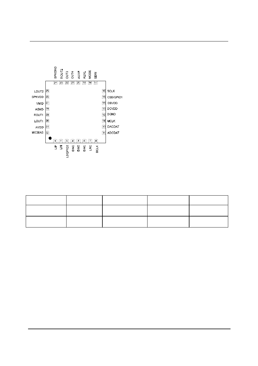
PIN CONFIGURATION
ORDERING INFORMATION
ORDER CODE
TEMPERATURE
RANGE
PACKAGE
MOISTURE
SENSITIVITY LEVEL
PEAK SOLDERING
TEMPERATURE
WM8976GEFL/V
-25
∞C to +85∞C
32-pin QFN (5 x 5 mm)
(lead free)
MSL3
260
o
C
WM8976GEFL/RV
-25
∞C to +85∞C
32-pin QFN (5 x 5 mm)
(lead free, tape and reel)
MSL3
260
o
C
Note:
Reel quantity = 3,500
WM8976
Preliminary Technical Data
w
PTD Rev 2.0 February 2005
4
PIN DESCRIPTION
PIN
NAME
TYPE
DESCRIPTION
1
LIP
Analogue input
Left Mic Pre-amp positive input
2
LIN
Analogue input
Left Mic Pre-amp negative input
3
L2/GPIO2
Analogue input
Left channel line input/secondary mic pre-amp positive input/GPIO pin
4
DNC
Do not connect
Leave this pin floating
5
DNC
Do not connect
Leave this pin floating
6
DNC
Do not connect
Leave this pin floating
7
LRC
Digital Input / Output
DAC and ADC Sample Rate Clock
8
BCLK
Digital Input / Output
Digital Audio Port Clock
9
ADCDAT
Digital Output
ADC Digital Audio Data Output
10
DACDAT
Digital Input
DAC Digital Audio Data Input
11
MCLK
Digital Input
Master Clock Input
12
DGND
Supply
Digital ground
13
DCVDD
Supply
Digital core logic supply
14
DBVDD
Supply
Digital buffer (I/O) supply
15
CSB/GPIO1
Digital Input / Output
3-Wire MPU Chip Select / General purpose input/output 1
16
SCLK
Digital Input
3-Wire MPU Clock Input / 2-Wire MPU Clock Input
17
SDIN
Digital Input / Output
3-Wire MPU Data Input / 2-Wire MPU Data Input/Acknowledge
18
MODE
Digital Input
Control Interface Selection
19
AUXL
Analogue input
Left Auxillary input
20
AUXR
Analogue input
Right Auxillary input
21
OUT4
Analogue Output
Buffered midrail Headphone pseudo-ground, or Right line output or MONO
mix output
22
OUT3
Analogue Output
Buffered midrail Headphone pseudo-ground, or Left line output
23
ROUT2
Analogue Output
Second right output, or BTL speaker driver positive output
24
SPKGND
Supply
Speaker ground (feeds speaker amp and OUT3/OUT4)
25
LOUT2
Analogue Output
Second left output, or BTL speaker driver negative output
26
SPKVDD
Supply
Speaker supply (feed speaker amp only)
27
VMID
Reference
Decoupling for ADC and DAC reference voltage
28
AGND
Supply
Analogue ground (feeds ADC and DAC)
29
ROUT1
Analogue Output
Headphone Output Right
30
LOUT1
Analogue Output
Headphone Output Left
31
AVDD
Supply
Analogue supply (feeds ADC and DAC)
32
MICBIAS
Analogue Output
Microphone Bias
Preliminary Technical Data
WM8976
w
PTD Rev 2.0 February 2005
5
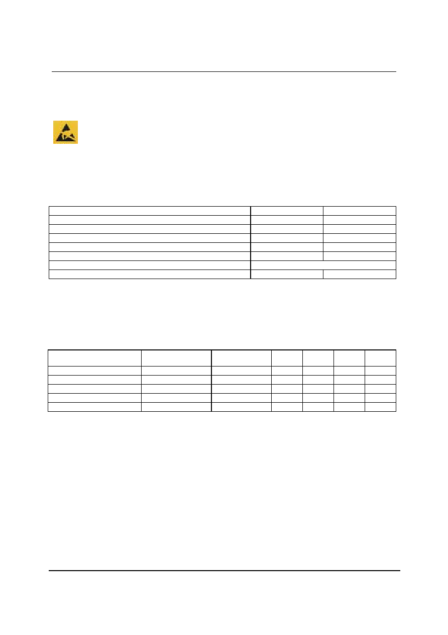
ABSOLUTE MAXIMUM RATINGS
Absolute Maximum Ratings are stress ratings only. Permanent damage to the device may be caused by continuously
operating at or beyond these limits. Device functional operating limits and guaranteed performance specifications are given
under Electrical Characteristics at the test conditions specified.
ESD Sensitive Device. This device is manufactured on a CMOS process. It is therefore generically susceptible
to damage from excessive static voltages. Proper ESD precautions must be taken during handling and storage
of this device.
Wolfson tests its package types according to IPC/JEDEC J-STD-020B for Moisture Sensitivity to determine acceptable storage
conditions prior to surface mount assembly. These levels are:
MSL1 = unlimited floor life at <30
∞C / 85% Relative Humidity. Not normally stored in moisture barrier bag.
MSL2 = out of bag storage for 1 year at <30
∞C / 60% Relative Humidity. Supplied in moisture barrier bag.
MSL3 = out of bag storage for 168 hours at <30
∞C / 60% Relative Humidity. Supplied in moisture barrier bag.
The Moisture Sensitivity Level for each package type is specified in Ordering Information.
CONDITION
MIN
MAX
DBVDD, DCVDD, AVDD supply voltages
-0.3V
+3.63V
SPKVDD supply voltage
-0.3V
+7V
Voltage range digital inputs
DGND -0.3V
DVDD +0.3V
Voltage range analogue inputs
AGND -0.3V
AVDD +0.3V
Operating temperature range, T
A
-25
∞C
+85
∞C
Storage temperature prior to soldering
30
∞C max / 85% RH max
Storage temperature after soldering
-65
∞C
+150
∞C
Notes
1.
Analogue and digital grounds must always be within 0.3V of each other.
2.
All digital and analogue supplies are completely independent from each other.
RECOMMENDED OPERATING CONDITIONS
PARAMETER
SYMBOL
TEST
CONDITIONS
MIN
TYP
MAX
UNIT
Digital supply range (Core)
DCVDD
1.62
3.6
V
Digital supply range (Buffer)
DBVDD
1.8
3.6
V
Analogue core supply range
AVDD
2.5
3.6
V
Analogue output supply range
SPKVDD
2.5
5.5
V
Ground
DGND,AGND, SPKGND
0
V