 | –≠–ª–µ–∫—Ç—Ä–æ–Ω–Ω—ã–π –∫–æ–º–ø–æ–Ω–µ–Ω—Ç: WM9709 | –°–∫–∞—á–∞—Ç—å:  PDF PDF  ZIP ZIP |
Document Outline
- WM9709
- AC-link Interface Audio DAC
- DESCRIPTION
- FEATURES
- APPLICATIONS
- BLOCK DIAGRAM
- PIN CONFIGURATION
- ORDERING INFORMATION
- PIN DESCRIPTION
- ABSOLUTE MAXIMUM RATINGS
- DC ELECTRICAL CHARACTERISTICS
- AC ELECTRICAL CHARACTERISTICS
- TERMINOLOGY
- SERIAL INTERFACE TIMINGS
- COLD RESET
- WARM RESET
- CLOCK SPECIFICATIONS
- DATA OUTPUT AND INPUT TIMES
- ATE IN CIRCUIT TEST MODE
- SIGNAL RISE AND FALL TIMES
- DIGITAL FILTER RESPONSE
- DEVICE DESCRIPTION
- INTRODUCTION
- AC-LINK LOW POWER MODE
- AC-LINK AUDIO INPUT FRAME (SDATAIN)
- AC-LINK AUDIO OUTPUT FRAME (SDATAOUT)
- AC-LINK DIGITAL SERIAL INTERFACE PROTOCOL
- CONTROL AND DATA INTERFACE
- SERIAL INTERFACE REGISTER MAP DESCRIPTION
- SERIAL INTERFACE REGISTER MAP
- RECOMMENDED EXTERNAL COMPONENTS
- RECOMMENDED EXTERNAL COMPONENT VALUES
- RECOMMENDATIONS FOR 3.3V OPERATION
- RECOMMENDATIONS FOR EXTERNAL FILTER
- RECOMMENDATIONS FOR MINIMISING POWER UP/DOWN èCLICKSê
- PACKAGE DIMENSIONS
- IMPORTANT NOTICE
- ADDRESS
w
WM9709
AC-link Interface Audio DAC
WOLFSON MICROELECTRONICS plc
w :: www.wolfsonmicro.com
Production Data, February 2003, Rev 1.3
Copyright
2003 Wolfson Microelectronics plc
DESCRIPTION
The WM9709 is a low cost, high-quality stereo audio DAC.
It utilises the Intel specified AC-link audio interface protocol,
allowing a pair of audio output channels to be added to any
AC link compliant controller device at minimal board area
and external component cost.
The WM9709 device supports 48ks/s sample rates when
operated at the normal AC link rate. The WM9709 supports
a revision 1.03 AC '97 AC-link interface, the device acting
as a master in normal operation.
The ID pin can be used to select which data slots on the
AC-link are to be used as input to the DAC. This allows 3 x
WM9709 to be used with a single controller that supports 6
channel sound, to output surround sound audio signals.
When supporting surround, centre or LFE channels, the
WM9709 behaves as a slave device.
The WM9709 device is footprint compatible with the
WM9708 codec, allowing simple swapping between DAC
and full codec features on the same board. The WM9709 is
packaged in a 20-pin SSOP.
FEATURES
∑
20-Bit
Stereo
DAC
∑
Audio
Performance
-
102dB SNR (`A' weighted at 48kHz)
-
-95dB
THD
∑
Revision 1.03 or higher AC'97 AC-link interface support.
∑
3.3V or mixed 3V digital, 5V analogue operation
∑
20-Pin
SSOP
Package
∑
Minimal external component cost
∑
Support for surround and centre/LFE channels
APPLICATIONS
∑
Notebook
PC
∑
PC sound cards
∑
Motherboards
∑
Custom
sound
applications
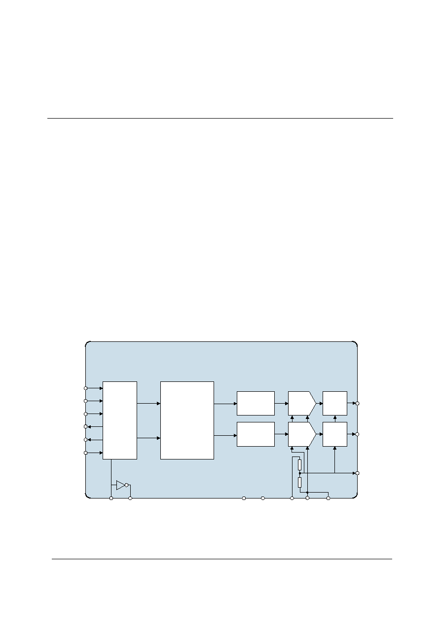
BLOCK DIAGRAM
LINEOUTR
SERIAL
INTERFACE
SDATAOUT
LINEOUTL
SIGMA
DELTA
MODULATOR
SDATAIN
BITCLK
SIGMA
DELTA
MODULATOR
DIGITAL FILTERS
DVDD
AGND
DGND
LOW
PASS
FILTER
LOW
PASS
FILTER
CAP
RIGHT
DAC
LEFT
DAC
AGND
AVDD
SYNC
RESETB
XTLIN XTLOUT
ID
w
WM9709
WM9709
Production Data
w
PD Rev 1.3 February 2003
2
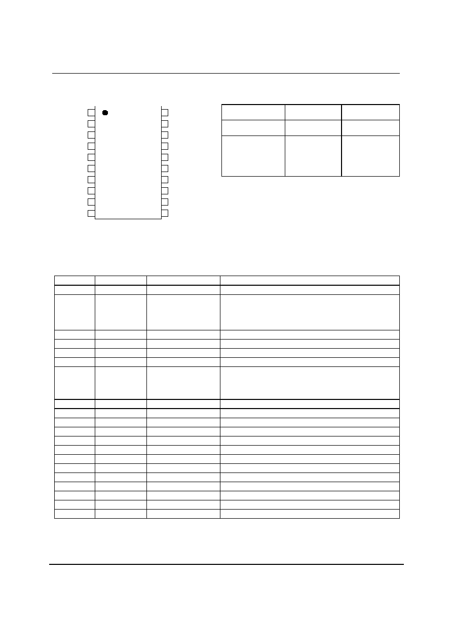
PIN CONFIGURATION
ORDERING INFORMATION
DEVICE TEMP.
RANGE
PACKAGE
WM9709CDS 0
o
to 70
o
C
20-pin SSOP
WM9709CDS/R 0
o
to 70
o
C 20-pin
SSOP
Tape and Reel
330mm Reel
16mm wide tape
2000 units/reel
12
11
5
6
7
1
2
3
4
8
9
10
DVDD
ID
NC
LINEOUTR
LINEOUTL
CAP
NC
NC
AVDD
AGND
RESETB
XTLOUT
SDATAOUT
XTLIN
SYNC
AGND
SDATAIN
DGND
NC
BITCLK
13
14
15
16
17
18
19
20
PIN DESCRIPTION
PIN NAME
TYPE
DESCRIPTION
1
RESETB
Digital input
NOT reset input (active low, resets digital circuitry)
2
ID
Digital input
AC link Data slot select.
Low = Normal stereo (slots 3,4),
High = Surround (slots 7,8),
High impedance (Z) = LFE and centre (slots 6,9)
3
DVDD
Supply
Digital positive supply
4
XTLIN
Digital input
Clock crystal connection or clock input (XTAL not used)
5
XTLOUT
Digital output
Clock crystal connection
6
SDATAOUT
Digital input
Serial data input
7
BITCLK Digital
output
(master)
Or digital input (slave)
Serial interface clock output to AC-link controller if ID pin held
low (WM9709 is master).
Serial interface clock input from AC-link master if ID pin held
either high or high impedance (WM9709 is slave).
8
DGND Supply
Digital
ground
supply
9
SDATAIN
Digital output
Serial data output to AC-link controller
10
SYNC
Digital input
Serial interface sync pulse from AC-link controller
11
AGND
Supply
Analogue ground supply, chip substrate
12
NC
No
internal
connection
13
NC
No
internal
connection
14
CAP
Analogue input
Reference input/output; internal divider generates midrail
15
NC
No
internal
connection
16
LINEOUTL
Analogue output
Main analogue output for left channel
17
LINEOUTR
Analogue output
Main analogue output for right channel
18
NC
No
internal
connection
19
AVDD Supply
Analogue
positive
supply
20
AGND
Supply
Analogue ground supply, chip substrate
Production Data
WM9709
w
PD Rev 1.3 February 2003
3
ABSOLUTE MAXIMUM RATINGS
Absolute Maximum Ratings are stress ratings only. Permanent damage to the device may be caused by continuously operating at
or beyond these limits. Device functional operating limits and guaranteed performance specifications are given under Electrical
Characteristics at the test conditions specified.
ESD Sensitive Device. This device is manufactured on a CMOS process. It is therefore generically susceptible
to damage from excessive static voltages. Proper ESD precautions must be taken during handling and storage
of this device.
CONDITION
MIN MAX
Digital supply voltage
-0.3V +7V
Analogue supply voltage
-0.3V +7V
Voltage range digital inputs
DGND -0.3V
DVDD +0.3V
Voltage range analogue inputs
AGND -0.3V
AVDD +0.3V
Operating temperature range, T
A
0
o
C +70
o
C
Storage temperature prior to soldering
30
o
C max / 85% RH max
Storage temperature after soldering
-65
o
C +150
o
C
Package body temperature (soldering, 10 seconds)
+240
o
C
Package body temperature (soldering, 2 minutes)
+183
o
C
WM9709
Production Data
w
PD Rev 1.3 February 2003
4
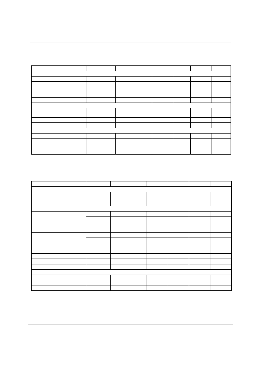
DC ELECTRICAL CHARACTERISTICS
Test Conditions:
AVDD = 5V, AGND = 0V, DVDD = 3.3V, DGND = 0V, T
A
= 25
o
C, unless otherwise stated.
PARAMETER SYMBOL
TEST
CONDITIONS
MIN
TYP
MAX
UNIT
Supply Ranges
Digital supply range
DVDD
-10%
3.3
+10% V
Analogue supply range
AVDD
-10%
3.3 to 5.0
+10%
V
Digital ground
DGND
0
V
Analogue ground
AGND
0
V
Difference DGND to AGND
-0.3
0
+0.3
V
Supply Currents
Analogue supply current
DVDD=3.3V,
AVDD = 5V
12.5
20 mA
Analogue supply current
DVDD, AVDD = 3.3V
11
mA
Digital supply current
DVDD, AVDD = 3.3V
5
8 mA
Digital Logic Levels (DVDD = 3.3)
Input LOW level
V
IL
DGND - 0.3
0.25
DVDD
V
Input HIGH level
V
IH
0.75
DVDD
DVDD + 0.3
V
Output LOW
V
OL
ILOAD = 1mA
0.1
DVDD
V
Output HIGH
V
OH
ILOAD = 1mA
0.9
DVDD
V
AC ELECTRICAL CHARACTERISTICS
Test Conditions:
AVDD = 5V, AGND = 0V, DVDD = 3.3V, DGND = 0V, T
A
= 25
o
C, unless otherwise stated.
PARAMETER SYMBOL
TEST
CONDITIONS
MIN
TYP
MAX
UNIT
Reference Levels
Reference input/output
CAP
AVDD/2
≠
25mV
AVDD/2 AVDD/2
+
25mV
CAP impedance
5 k
DAC Circuit Specifications (48kHz Sample Rate)
AVDD = 5V
95
102
dB
SNR A-weighted (Note 1,2)
AVDD = 3.3V
99
dB
DNR AVDD
=
5V 95 102 dB
Dynamic Range
AVDD = 3.3V
99
dB
AVDD=5V 0.95
1.0
1.05
Vrms
Full scale output voltage into
10k
load
AVDD=3.3V 0.66 Vrms
THD
0dBfs
-95
-85
dB
Channel Separation
95
102
dB
Channel Matching
-0.35
0
0.35
dB
PSRR
1kHz, 10
µ
F on CAP pin
46 dB
Output offset wrt CAP voltage
-30 0 30 mV
Clock Frequency Range
Crystal clock
24.576 MHz
BITCLK frequency
12.288 MHz
SYNC frequency
48.0 kHz
Production Data
WM9709
w
PD Rev 1.3 February 2003
5
Notes:
1.
Ratio of output level with 1kHz full scale input, to the output level with all zeros into the digital input, measured `A'
weighted over a 20Hz to 20kHz bandwidth.
2.
All performance measurements done with 20kHz low pass filter, and where noted an A-weight filter. Failure to use
such a filter will result in higher THD+N and lower SNR and Dynamic Range readings than are found in the Electrical
Characteristics. The low pass filter removes out of band noise; although it is not audible it may affect dynamic
specification values.
3.
SNR measured with A-weight filter is typically 2dB better than with CCIR2k filter, or 20kHz low pass filter.
TERMINOLOGY
1.
Signal-to-noise ratio (dB) - SNR is a measure of the difference in level between the full scale output and the output
with no signal applied. (No Auto-zero or Automute function is employed in achieving these results).
2.
Channel Separation (dB) - Also known as Cross-Talk. This is a measure of the amount one channel is isolated from
the other. Normally measured by sending a full scale signal down one channel and measuring the other.
3.
Dynamic range (dB) - DNR is a measure of the ratio between the largest and smallest usable signals. Normally a
THD+N measurement at 60dB below full scale. The measured signal is then corrected by adding the 60dB to it. (e.g.
THD+N @ -60dB= 42dB, DNR= 102dB).
4.
THD+N (dB) - THD+N is a ratio, of the rms values, of (Noise + Distortion)/Signal.
SERIAL INTERFACE TIMINGS
Test Conditions:
AVDD = 5V, AGND = 0V, DVDD = 3.3V, DGND = 0V, TA
= 25
o
C, unless otherwise stated. All
measurements are taken at 10% to 90% VDD, unless otherwise stated.
All the following timing information is guaranteed by design, but not tested in production.
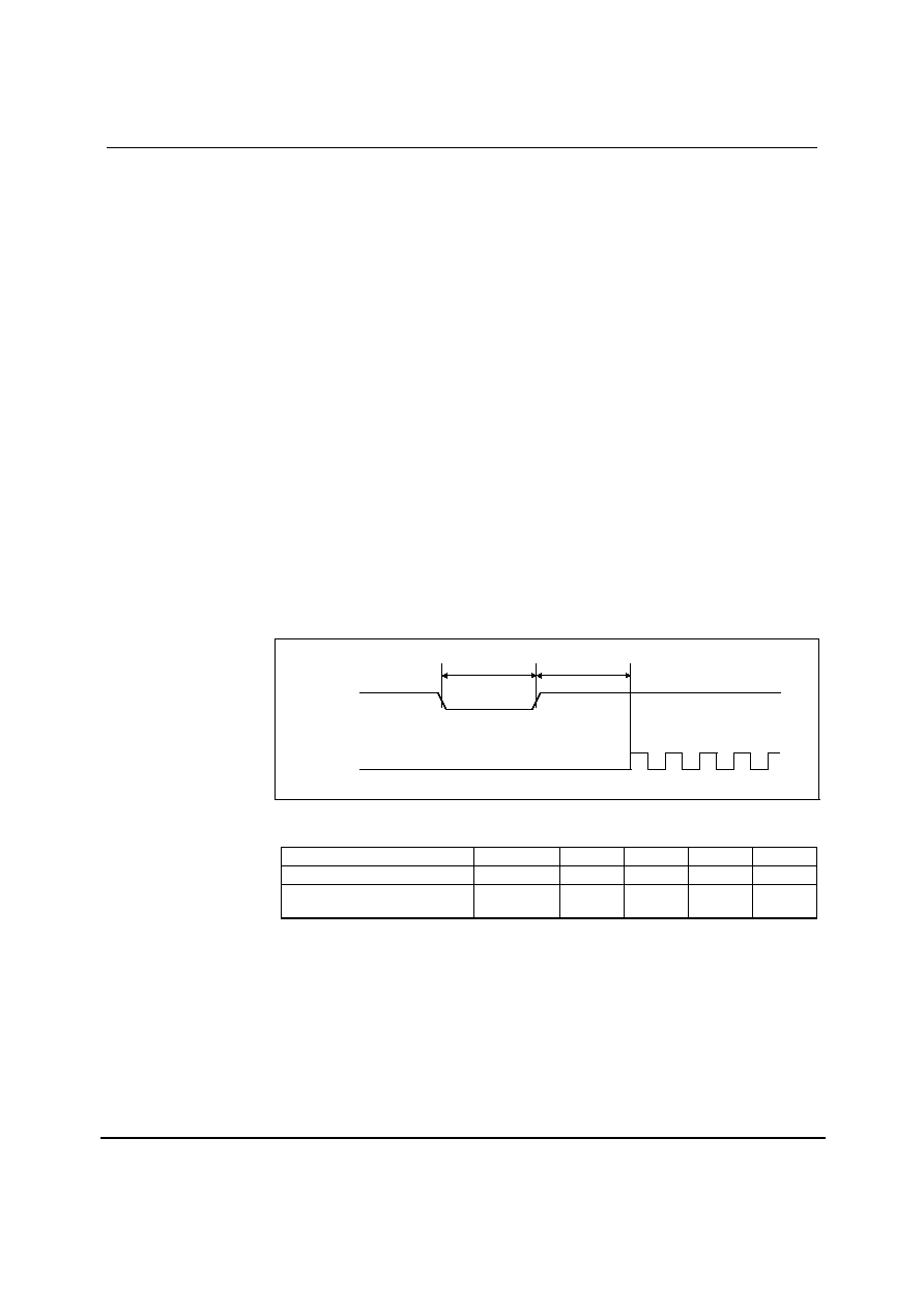
COLD RESET
RESETB
BITCLK
t
RST_LOW
t
RST2CLK
Figure 1 Cold Reset Timing
PARAMETER SYMBOL
MIN
TYP
MAX
UNIT
RESETB active low pulse width
t
RST_LOW
1.0
µ
s
RESETB inactive to BITCLK
startup delay
t
RST2CLK
162.8
ns
WARM RESET
Not supported by WM9709